1. 3.2.4-Digital to Analog conversion:
3.2.4.1-Introduction:
Connecting digital circuitry to sensor devices is simple if the sensor devices are inherently
digital themselves. Switches, relays, and encoders are easily interfaced with gate circuits due to
the on/off nature of their signals. However, when analog devices are involved, interfacing
becomes much more complex. What is needed is a way to electronically translate analog signals
into digital (binary) quantities, and vice versa. An analog-to-digital converter, or ADC,
performs the former task while a digital-to-analog converter, or DAC, performs the latter.
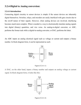
An ADC inputs an analog electrical signal such as voltage or current and outputs a binary
number. In block diagram form, it can be represented as such:
Figure-(3.2.4.1.1)
A DAC, on the other hand, inputs a binary number and outputs an analog voltage or current
signal. In block diagram form, it looks like this:
Figure-(3.2.4.1.2)
2. Together, they are often used in digital systems to provide complete interface with analog
sensors and output devices for control systems such as those used in automotive engine
controls:
Figure-(3.2.4.1.3)
It is much easier to convert a digital signal into an analog signal than it is to do the reverse.
3.2.4.2-The R/2nR DAC:
This DAC circuit, otherwise known as the binary-weighted-input DAC, is a variation on the
inverting summer op-amp circuit. If you recall, the classic inverting summer circuit is an
operational amplifier using negative feedback for controlled gain, with several voltage inputs
and one voltage output. The output voltage is the inverted (opposite polarity) sum of all input
voltages:
Figure-(3.2.4.1.4)
3. For a simple inverting summer circuit, all resistors must be of equal value. If any of the input
resistors were different, the input voltages would have different degrees of effect on the output,
and the output voltage would not be a true sum. Let's consider, however, intentionally setting
the input resistors at different values. Suppose we were to set the input resistor values at
multiple powers of two: R, 2R, and 4R, instead of all the same value R:
Figure-(3.2.4.1.5)
Starting from V1 and going through V3, this would give each input voltage exactly half the
effect on the output as the voltage before it. In other words, input voltage V1 has a 1:1 effect on
the output voltage (gain of 1), while input voltage V2 has half that much effect on the output (a
gain of 1/2), and V3 half of that (a gain of 1/4). These ratios are were not arbitrarily chosen:
they are the same ratios corresponding to place weights in the binary numeration system. If we
drive the inputs of this circuit with digital gates so that each input is either 0 volts or full supply
voltage, the output voltage will be an analog representation of the binary value of these three
bits.
Figure-(3.2.4.1.6)
4. If we chart the output voltages for all eight combinations of binary bits (000 through 111) input to this circuit,
we will get the following progression of voltages:
Binary Output Voltage
000 0.00 V
001 -1.25 V
010 -2.50 V
011 -3.75 V
100 -5.00 V
101 -6.25 V
110 -7.50 V
111 -8.75 V
If we wish to expand the resolution of this DAC (add more bits to the input), all we need to do
is add more input resistors, holding to the same power-of-two sequence of values:
Figure-(3.2.4.1.7)
It should be noted that all logic gates must output exactly the same voltages when in the "high"
state. If one gate is outputting +5.02 volts for a "high" while another is outputting only +4.86
volts, the analog output of the DAC will be adversely affected. Likewise, all "low" voltage
levels should be identical between gates, ideally 0.00 volts exactly. It is recommended that
CMOS output gates are used, and that input/feedback resistor values are chosen so as to
minimize the amount of current each gate has to source or sink.