SlideShare une entreprise Scribd logo
1  sur  37
Télécharger pour lire hors ligne


            CDE’2013


        9th
Spanish
Conference

         On
Electron
Devices


        Palacio
de
Congresos

           Conde
Ansúrez


          Valladolid,
Spain

        February
12‐14,

2013


           www.cde2013.es


                                    COMMITTEES


        LOCAL
COMMITTEE


        Luis
Alberto
Bailón
Vega

        Dpt.

Electricidad
y
Electrónica,
UVa

        Ismael
Barba
García

        Dpt.

Electricidad
y
Electrónica,
UVa

        Helena
Castán
Lanaspa
 (chair)

        Dpt.

Electricidad
y
Electrónica,
UVa

        Salvador
Dueñas
Carazo

        Dpt.

Electricidad
y
Electrónica,
UVa

        Héctor
García
García
           (papers)

        Dpt.

Electricidad
y
Electrónica,
UVa

        Miguel
Ángel
González
Rebollo

        Dpt.
Física
de
la
Materia
Condensada,
Cristalografía
y
Mineralogía,
UVa

        Ana
Grande
Sáez

        Dpt.

Electricidad
y
Electrónica,
UVa

        Juan
Jiménez
López

        Dpt.
Física
de
la
Materia
Condensada,
Cristalografía
y
Mineralogía,
UVa

        Ana
Cristina
López
Cabeceira

        Dpt.

Electricidad
y
Electrónica,
UVa

        Luis
Alberto
Marqués
Cuesta

        Dpt.

Electricidad
y
Electrónica,
UVa

        José
Represa
Fernández

        Dpt.

Electricidad
y
Electrónica,
UVa


                                                                              i


ADVISORY
COMMITTEE


José
Millán
‐
IMB‐CNM‐CSIC

 (CDE
Advisory
Committee
Chair)

Juan
A.
de
Agapito
‐
Universidad
Complutense
de
Madrid

Xavier
Aymerich
‐
Universidad
Autónoma
de
Barcelona

Luis
Bailón
‐
Universidad
de
Valladolid

Fernando
Briones
‐
IMM‐CNM‐CSIC

Enrique
Calleja
‐
Universidad
Politécnica
de
Madrid
/
ISOM

Pedro
Cartujo
‐
Universidad
de
Granada

Luis
Castañer
‐
Universidad
Politécnica
de
Cataluña

Xavier
Correig
‐
Universidad
Rovira
i
Virgili

Eugenio
García
Moreno
‐
Universidad
de
las
Islas
Baleares

Javier
Gracia
‐
CEIT

F.
Javier
Gutiérrez
Monreal
‐
IFA‐CSIC

Antonio
Luque
‐
Universidad
Politécnica
de
Madrid
/
IES

Joan
Ramón
Morante
‐
Universidad
de
Barcelona
/
IREC

Elías
Muñoz
Merino
‐
Universidad
Politécnica
de
Madrid
/
ISOM

Daniel
Pardo
‐
Universidad
de
Salamanca

Juan
Piqueras
‐
Universidad
Autónoma
de
Madrid

Francisco
Serra
‐
Universidad
Autónoma
de
Barcelona
/
CNM‐CSIC


TECHNICAL
COMMITTEE


Antonio
García
Loureiro
‐
Universidad
de
Santiago
de
Compostela

Ramón
Alcubilla
‐
Universidad
Politécnica
de
Catalunya

Carlos
Algora
‐
Universidad
Politécnica
de
Madrid
/
IES

Angel
Luis
Alvarez
Castillo
‐
Universidad
Rey
Juan
Carlos

Javier
Berganzo
‐
IKERLAN

Carles
Cané
‐
IMB‐CNM‐CSIC

Fernando
Calle
‐
Universidad
Politécnica
de
Madrid
/
ISOM

Enrique
Castaño
‐
CEIT

Salvador
Dueñas
Carazo
‐
Universidad
de
Valladolid

Ignacio
Garcés
‐
Universidad
de
Zaragoza

Tomás
González
‐
Universidad
de
Salamanca

María
Jesús
Hernández
‐
Universidad
Autónoma
de
Madrid

Carmen
Horrillo
‐
IFA‐CSIC

Pedro
Ibañez
Ereño
‐
ROBOTIKER

Fernando
López
‐
Universidad
Carlos
III

Juan
A.
López
Villanueva
‐
Universidad
de
Granada

Lluis
Marsal
‐
Universidad
Rovira
i
Virgili

Ignacio
Mártil
de
la
Plaza
‐
Universidad
Complutense
de
Madrid

Enrique
Maset
‐
Universidad
de
Valencia

Montserrat
Nafria
‐
Universidad
Autónoma
de
Barcelona

Isabel
Obieta
Villalonga
‐
INASMET

Rodrigo
Picos
‐
Universidad
de
las
Islas
Baleares

José
Manuel
Quero
Reboul
‐
Universidad
de
Sevilla
/
AICIA

José
María
Ripalda
Cobian
‐
IMM‐CNM‐CSIC

Albert
Romano
Rodríguez
‐
Universidad
de
Barcelona


ii


             SUPPORTED
BY:


        TECHNICAL
CO‐SPONSORSHIP:


                                iii


iv


                                 WELCOME
LETTER


The
 9th
 Spanish
 Conference
 on
 Electron
 Devices
 brings
 together
 the
 work
 of
 both

research
groups
and
companies
on
the
field
of
electronic
devices.
This
edition
will
take

place
 from
 the
 12th

 to
 the
 14th
 of
 February
 of
 2013,
 in
 Valladolid,
 carrying
 on
 with
 a

series
of
previous
events
in
Palma
de
Mallorca
(2011),
Santiago
de
Compostela
(2009),

El
 Escorial
 (Madrid,
 2007),
 Tarragona
 (2005),
 Calella
 de
 la
 Costa
 (2003),
 Granada

(2001),
Madrid
(1999)
and
Barcelona
(1997).

As
usual,
the
Conference
program
consists
of
invited
and
contributed
papers
organized

in
the
topic
sessions.
The
Congress
will
conclude
with
a
workshop
about
Solar
Energy,

which
will
be
composed
by
7
talks,
22
posters
and
a
round
table
with
the
participation

of
companies
from
the
Solar
Energy
Cluster
of
Castilla
and
León.

Just
before
the
CDE

conference
opening,
a
Mini
Colloquium
(MQ)
of
Electron
Device
Society
(EDS)
will
take

place
at
the
same
venue
as
CDE,
without
additional
registration
fees.
In
this
way,
all
the

CDE
participants
may
attend
to
both
events.


The
 total
 number
 of
 contributions
 is
 122:
 2
 plenary
 talks,
 11
 invited
 talks,
 25

talks,
and
84
posters,
distributed
in
the
following
topics:

             S1
       Process
technology
for
devices
and
simulation

             S2
       Device
modeling

             S3
       Sensors,
actuators
and
micro/nano
systems

             S4
       Emerging
devices

             S5
       Characterization
and
reliability

             S6
       Solar
energy:
thermal
and
photovoltaic
devices


Most
of
the
contributions
presented
at
this
conference
come
from
Spanish
Universities

and
Research
Centers.
30
%
of
them
are
fruit
of
the
cooperation
between
Spanish
and

foreigner
 institutions
 and
 15%
 of
 the
 works
 come
 from
 researchers
 of
 foreign

countries.
 It
 is
 important
 to
 point
 out
 the
 high
 number
 of
 collaborations
 among

different
 institutions
 (41%),
 so
 indicating
 the
 increase
 of
 cooperative
 work
 of
 the

Spanish
research
groups
in
the
CDE
scope.


Because
 of
 the
 delicate
 economic
 situation,
 fundings
 to
 the
 Congress
 have
 been

significantly
 reduced
 compared
 to
 previous
 years,
 so
 this
 issue
 will
 necessarily
 be

austere
 without
 any
 impact
 on
 the
 scientific
 quality.
 We
 appreciate
 in
 advance
 the

understanding
 of
 this
 forced
 sobriety
 and
 we
 are
 convinced
 that
 in
 order
 to
 address

these
difficulties
we
must
use
all
our
resources
to
ensure
that
science
and
progress
will

continue
developing.


                                                                                            v

As
Vladimir
Nabokov
says:
“there
is
no
science
without
fancy”,
although
Hans
Magnus

Enzensberger
 believes
 that
 "poetry
 of
 science
 is
 not
 at
 ground
 level,
 but
 comes
 from

the
 deepest
 layers".
 We
 have
 organized
 this
 conference
 with
 the
 belief
 that
 scientific

research
is
a
great
privilege
for
the
human
being.


We
would
like
to
thank
all
the
supports
received
from
the
following
organizations
and

companies:
The
University
of
Valladolid,
the
Government
of
Castilla
y
León,
the
City
of

Valladolid,
the
IEEE
Spanish
Section,
and
Instrumentos
de
Medida
S.L.
We
extend
our

thanks
to
the
CDE
Advisory
and
Technical
Committees,
as
well
as
to
the
organizers
of

the
CDE
from
previous
editions.

Our
very
special
thank
to
the
CDE
Advisory
Committee
Chair,
Prof.
José
Millán.


                                                      The
Conference
Local
Committee


                    Contribu)ons
from
Spanish
Research

                          Centers
and
Universi)es

        16

        14

        12

        10

          8

          6

          4

          2

          0


                     Contribu)ons
form
Foreign
Countries

          8


              6


              4


              2


               0


vi


                             CDE
2013


PROGRAM

Tuesday,
Feb.
12,
2013

14.00
h
‐

20.00
h
  REGISTRATION

14.00
h
–
18.00
h

  Mini
 Colloquium
 EDS.
 Prof.
 Benjamín
 Íñiguez,
 Univ.
 Rovira
 I

                     Virgili,
Chair

18.30
h
–
20.00
h

  WELCOME
RECEPTION


20.00
h
‐

     
    RUTA
DE
TAPAS


Wednesday,
Feb.
13,
2013

8.00
h
–
8.30
h

    REGISTRATION

8.30
h
–
8.45
h

    OPENING:
Prof.
José
Millán,
CDE
Advisory
Committee
Chair

8.45

h
–
9.30
h

   PLENARY
TALK:
Prof.
Emilio
Lora‐Tamayo,
CSIC
Chair

9.30
h
‐
11.35
h

   SESSION
1:
Process
technology
for
devices
and
simulation

11.35
h
–
12.00
h
   COFFEE
BREAK

12.00
h
–
14.05
h

  SESSION
2:
Device
modeling

14.05
h
–
15.30
h
   LUNCH

15.30
h
–
17.35
h
   SESSION
3:
Sensors,
actuators
and
micro/nano
systems

17.35
h
–
18.00
h
   COFFEE
BREAK


                                                  CDE
Advisory
Committee
Meeting

18.00
h
–
19.30
h

  POSTER:
SESSIONS
1
‐
5

19.30
h
‐

20.30
h
  CLASSICAL
MUSIC
PERFORMANCE

21.30
h
‐

     
    GALA
DINNER

                    EDS
Chapter
of
the
Year
Award


                                                   Award

Thursday,
Feb.
14,
2013

8.00
h
–
10.05
h

     SESSION
4:
Emerging
devices
       

10.05
h
‐
10.30
h

    COFFEE
BREAK

10.30
h
–
12.35
h
     SESSION
5:
Characterization
and
reliability


12.35
h
‐
     
       WORKSHOP:
SOLAR
ENERGY

        12.35
h
–
14.00
h

  POSTER:
SESSION
6

        14.00
h
–
15.30
h
   LUNCH


       15.30
h
–
16.15
h
   PLENARY
TALK:
Prof.
Carlos
Algora,
IES‐UPM


       16.15
h
–
18.15
h
   SESSION
6:
Solar
Energy:
thermal
and
photovoltaic
devices


       18.15
h
–
18.30
h
   COFFEE
BREAK


       18.30
h
–
19.45
h

  ROUND
TABLE.
Prof.
Juan
Jiménez,
Univ.
Valladolid.
Chair


       19.45
h
–
20.00
h

  CLOSING
REMARKS
 

                                                    EDS:
Best
Student
Award


OUT
OF
PROGRAM:

Friday,
Feb.
15,
2013


(for
the
participants
staying
in
Valladolid)

Sightseeing
on
foot
and
museums.


                                                                          CDE2013
 1


Tuesday,
Feb.
12,
2013


 14.00
h
‐

20.00
h
    Palacio
de
Congresos
Conde
Ansúrez,
third
floor

                        REGISTRATION


 14.00
h
–
18.00
h

    Auditorium,
Palacio
de
Congresos
Conde
Ansúrez,
third
floor

                        EDS
MINI
COLLOQUIUM.
Prof.
Benjamín
Íñiguez,
Univ.
Rovira
I

                        Virgili.
Chair


 18.30
h
–
20.00
h

    Palacio
de
Santa
Cruz

                        WELCOME
 RECEPTION:
 Prof.
 Marcos
 Sacristán,
 Chancellor
 of

                    
   University
of
Valladolid


 20.00
h
‐

        
   RUTA
DE
TAPAS:
Tapas
bars
in
the
city
center


Wednesday,
Feb.
13,
2013


 8.00
h
–
8.30
h

      Palacio
de
Congresos
Conde
Ansúrez,
third
floor

                        REGISTRATION


 8.30
h
–
8.45
h

      Auditorium,
Palacio
de
Congresos
Conde
Ansúrez,
third
floor

                        OPENING:
Prof.
José
Millán,
CDE
Advisory
Committee
Chair


 9.30
h
‐
11.35
h

     Auditorium,
Palacio
de
Congresos
Conde
Ansúrez,
third
floor

                        SESSION
 1:
 Process
 technology
 for
 devices
 and

                        simulation

                        Chairperson:
Prof.
Javier
Martínez
Rodrigo


9.30
h
–
9.55
h

O.1.1.
 Invited:
 Thin
Dielectric
Films
Grown
by
Atomic
Layer
Deposition:
Properties

and
Applications.

Francesca
Campabadal,
J.M.
Rafí,
M.B.
González,
M.Zabala,
O.
Beldarrain,
M.C.
Acero

and
M.
Duch

Institut
de
Microelectrònica
de
Barcelona,
IMB‐CNM
(CSIC).


9.55
h
–
10.15
h

O.1.2.
 Plasma
 oxidation
 of
 metallic
 Gd
 deposited
 on
 silicon
 by
 high
 pressure

sputtering
as
high
permittivity
dielectric


      R38

M.
A.
Pampillón1,
P.
C.
Feijoo1,
E.
San
Andrés1,
J.
L.
G.
Fierro2

1
 Departamento
 de
 Física
 Aplicada
 III
 (Electricidad
 y
 Electrónica).
 Facultad
 de


Ciencias
Físicas.
Universidad
Complutense
de
Madrid.
28040,
Madrid,
Spain.


2
Instituto
de
Catálisis
y
Petroleoquímica.
CSIC.
Cantoblanco.
28049,
Madrid,
Spain.


2
       PROGRAMA


10.15
h
–
10.35
h

O.1.3.
Use
of
PMMA
to
obtain
Graphene
layers


       R93

A.
 Bosca 1,
 
 D.
 Lopez‐Romero1,
 S.
 Alvarez‐Garcia2,
 A.
 de
 Andres2,
 J.
 Pedros1,
 J.


Martinez1
and
F.
Calle1

1
Instituto
de
Sistemas
Optoelectrónicos
y
Microtecnología,
Universidad
Politécnica


de
Madrid,
28040
Madrid,
Spain.

2
Instituto
de
Ciencia
de
Materiales
de
Madrid,
Consejo
Superior
de
Investigaciones


Científicas,
28049
Madrid,
Spain.


10.35
h
–
10.55
h

O.1.4.
Nanodevice
simulations
on
CloudStack


       R98

F.
Gomez‐Folgar,
E.
Comesaña,
R.
Valin,
A.
Garcia‐Loureiro,
T.
F.
Pena.

Centro
 de
 Investigación
 en
 Tecnoloxías
 da
 Información
 (CITIUS).
 Universidad
 de

Santiago
de
Compostela.


10.55
h
–
11.15
h

O.1.5.
 Direct‐write
 patterning
 of
 metals
 and
 reduced
 graphene
 oxide
 electrodes
 by

arc
erosion
for
organic
device
manufacturing


     R110

M.
 García‐Vélez,
 A.
 L.
 Alvarez,
 C.
 Coya,
 G.
 Alvarado,
 J.
 Jiménez‐Trillo1,
 X.
 Diéz‐
Betriú2,
A.
de
Andrés2

Dpt.
Tecnología
Electrónica,
ESCET,
Universidad
Rey
Juan
Carlos,
Móstoles,
28933

Madrid
(Spain)

1Dpt.
 Ingeniería
 de
 Circuitos
 y
 Sistemas,
 EUIT
 Telecomunicación,
 UPM,
 28031


Madrid
(Spain)

2Instituto
 de
 Ciencia
 de
 Materiales
 de
 Madrid,
 CSIC.
 Cantoblanco,
 28049
 Madrid


(Spain)


11.15
h
–
11.35
h

O.1.6.

Microscopic
modeling
of
interdiffusion
in
SiGe
alloys
       
     R117

Pedro
Castrillo,
Iván
Santos,
Ruth
Pinacho,
Emiliano
Rubio,
and
Martín
Jaraiz

Dpto.
 de
 Electrónica,
 Universidad
 de
 Valladolid,
 E.T.S.I.
 Telecomunicación,
 Paseo

Belén
15,
47011
Valladolid,
Spain.


11.35
h
–
12.00
h
     COFFEE
BREAK


 12.00
h
–
14.05
h

       Auditorium,
Palacio
de
Congresos
Conde
Ansúrez,
third
floor

                           SESSION
2:
Device
modeling

                           Chairperson:
Prof.
Juan
Antonio
López
Villanueva


12.00
h
–
12.25
h

O.2.1.
Invited:
Modeling
of
radiation
effects
in
MOSFETs

Jesús
Banqueri,
M.
A.
Carvajal
and
A.
J.
Palma

ECsens
(Electronic
and
Chemical
SENsing
Solutions),
Departamento
de
Electrónica

y
Tecnología
de
Computadores.
Universidad
de
Granada.


                                                                                CDE2013
 3


12.25
h
–
12.45
h

O.2.2.
 A
 new
 strategy
 to
 improve
 frequency
 performance
 of
 emerging
 devices

without
length
scaling


    R116

A.
Benali,
F.
L.
Traversa,
G.
Albareda,
M.
Aghoutaneb 1
and
X.
Oriols


Universitat
Autònoma
de
Barcelona,
08193,
Bellaterra,
Spain


1Universidad
Abdelmalek
Essaâdi,
93000,
Tetuán,
Morocco


12.45
h
–
13.05
h

O.2.3.
 Wide
 frequency
 band
 scalable
 modeling
 of
 3D
 embedded
 decoupling

capacitors

Hélène
Jacquinot1,
David
Denis2


      R22

1CEA,
LETI,
MINATEC
Campus,
17
rue
des
Martyrs,
38054
Grenoble.
France.


2IPDIA,
2
rue
de
la
Girafe,
14000
Caen.
France.


13.05
h
–
13.25
h

O.2.4.
Monte
Carlo
analysis
of
thermal
effects
in
Self‐Switching
Diodes
 
   R48

J.‐F.
Millithaler,
I.
Iñiguez‐de‐la‐Torre,
T.
González,
J.
Mateos


Departamento
 de
 Física
 Aplicada,
 Universidad
 de
 Salamanca,
 37008
 Salamanca,

Spain.


13.25
h
–
13.45
h

O.2.5.
OTFT
modeling:
development
and
implementation
in
EDA
tools
 
              R113

A.
Castro‐Carranza  1,
M.
Cheralathan1,
C.
Valla2,
M.
Estrada3,
A.
Cerdeira3,
F.
Poullet2,


G.
Depeyrot2,
B.
Iñiguez1
and
J.
Pallarès1

1Departament
 d’Enginyeria
 Electrònica
 (DEEEA),
 
 Universitat
 Rovira
 I
 Virgili


43007,
Tarragona,
Spain.


2DOLPHIN
Integration
GmbH,
F‐38242
Meylan,
France.


3Sección
 de
 Electrónica
 del
 Estado
 Sólido
 (SEES),
 CINVESTAV‐IPN,
 07360
 Mexico


D.F.,
Mexico.


13.45
h
–
14.05
h

O.2.6.

Analysis
of
Crossover
Point
and
Threshold
Voltage
for
Triple
Gate
MOSFET.


Dheeraj
Sharma
and
Santosh
Vishvakarma


     R62

Nanoscale
Devices,
VLSI/Circuit
and
System
Design
Lab,
Electrical
Engineering,


Indian
Institute
of
Technology,
Indore,
India.


14.05
h
–
15.30
h
    LUNCH


4
       PROGRAMA


15.30
h
–
17.35
h
       Auditorium,
Palacio
de
Congresos
Conde
Ansúrez,
third
floor

                          SESSION
3:
Sensors,
actuators
and
micro/nano
systems

                          Chairperson:
Prof.
Carmen
Horrillo


15.30
h
–
15.55
h

O.3.1.
Invited:
Sensors
and
Microsytems
for
the
Food
sector.


Carles
Cané.

Institut
de
Microelectrònica
de
Barcelona,
IMB‐CNM
(CSIC).


15.55
h
–
16.15
h

O.3.2.
Benzene
sensor
based
on
in‐situ
grown
ZnO
nanostructures
      
                   R47

J.
Gonzalez‐Chavarri,
I.
Castro‐Hurtado,
G.
G.
Mandayo,
and
E.
Castaño


Ceit
and
Tecnun,
P.
Manuel
Lardizabal
15,
20018,
San
Sebastian,
Spain


16.15
h
–
16.35
h

O.3.3.
Ceramic
Capacitive
Pressure
Sensor
based
on
LTCC
Technology


R65

Josep
 M.
 Fernández‐Sanjuán1,2,
 Núria
 Bonet2,
 Josep
 G.
 Rodríguez2,
 Francisco
 M.

Ramos1,2,
Javier
J.
Sieiro3,
José
M.
López‐Villegas3,
Albert
Cirera1

1MIND/IN2UB
Electronics
Department,
Universitat
de
Barcelona,
Martí
i
Franquès,


1,
Barcelona
08028,
Spain.

2FAE‐
Francisco
Albero
S.A.U.,
Rafael
Barradas
19,
L’Hospitalet
de
Llobregat
08908,


Spain.

3GRAF
 Electronics
 Department,
 Universitat
 de
 Barcelona,
 Martí
 i
 Franquès,
 1,


Barcelona
08028,
Spain.


16.35
h
–
16.55
h

O.3.4.
Microfluidics
applied
to
Love‐wave
devices
to
detect
biological
warfare
agents

in
dynamic
mode.


      R67

D.
 Matatagui1,
 J.
 Fontecha1,
 M.J.
 Fernández1,
 I.
 Gràcia2,
 C.
 Cané2,
 J.P.
 Santos1,
 M.C.

Horrillo1


1GRIDSEN,
CSIC,
Serrano
144,
28006
Madrid,
Spain


2Instituto
de
Microelectrónica
de
Barcelona,
CSIC,
Campus
UAB,
08193
Bellaterra,


Spain


16.55
h
–
17.15
h

O.3.5.
Electroosmotic
impulsion
device
for
integration
in
PCB‐MEMS


R96

Antonio
Luque,
José
M.
Soto,
Francisco
Perdigones,
Carmen
Aracil,
José
M.
Quero.

Dpto.
 Ingeniería
 Electrónica,
 Escuela
 Técnica
 Superior
 de
 Ingeniería,
 Universidad

de
Sevilla.
Av.
Descubrimientos
s/n

E41092
Sevilla.


17.15
h
–
17.35
h

O.3.6.
 Low
 power
 consumption
 single
 metal
 oxide
 nanowire
 based
 gas
 sensor

integrated
on
MEMS
Microhotplates


    R104

J.
 Samà1,
 R.
 Jiménez‐Díaz1,
 J.D.
 Prades1,
 O.
 Casals1,
 F.
 Hernandez‐Ramirez2
 3,
 J.

Santander4,
C.
Calaza4,

L.
Fonseca4,
C.
Cané4,
S.
Barth5,
A.
Romano‐Rodríguez1

                                                                                   CDE2013
 5


1
 MIND‐IN2UB‐Dept.
 Electronics,
 Universitat
 de
 Barcelona
 (UB),
 Martí
 i
 Franquès


1,
08028,
Barcelona,
Spain.


2
 Institut
 de
 Recerca
 en
 Energia
 de
 Catalunya,
 Jardins
 de
 les
 Dones
 de
 Negre
 1,


08930
Sant
Adrià
de
Besòs,
Spain


3
 Dept.
 Electronics,
 Universitat
 de
 Barcelona
 (UB),
 Martí
 i
 Franquès
 1,
 08028,


Barcelona,
Spain

4
 Institut
 
 de
 Microelectrònica
 de
 Barcelona,
 IMB‐CNM‐CSIC,
 08193
 Bellaterra,


Spain

5
Institute
of
Materials
Chemistry,
TU
Wien,
Getreidemarkt
9/165,
A‐1060
Vienna,


Austria.


17.35
h
–
18.00
h
        COFFEE
BREAK


    18.00
h
–
19.30
h

    Palacio
de
Congresos
Conde
Ansúrez,
second
floor

                           POSTER:
SESSIONS
1
‐
5


POSTER
‐
SESSION
1:
Process
technology
for
devices
and
simulation

P.1.1.
Gadolinium
scandate
by
high
pressure
sputtering
as
a
high‐k
dielectric


R5

P.C.
Feijoo,
M.A.
Pampillón,
E.
San
Andrés

Dpto.
 Física
 Aplicada
 III:
 Electricidad
 y
 Electrónica.
 Universidad
 Complutense
 de

Madrdid.
Av/Complutense
S/N.
28040
Madrid
(Spain).


P.1.2.
Effects
of
Ozone
Pre‐deposition
Treatment
on
GaSb
MOS
Capacitors


R13

Zhen
Tan,
Lianfeng
Zhao,
Ning
Cui,
Jing
Wang,
and
Jun
Xu

Tsinghua
National
Laboratory
for
Information
Science
and
Technology,
Institute
of

Microelectronics,
Tsinghua
University,
Beijing
100084,
P.R.China.


P.1.3.
 Towards
 high‐k
 integration
 with
 III‐V
 channels:
 interface
 optimization
 of

high
pressure
sputtered
Gd2O3
on
InP


R45

E.
San
Andrés,
M.
A.
Pampillón,
C.
Cañadilla,
P.
C.
Feijoo,
A.
del
Prado.

Departamento
 de
 Física
 Aplicada
 III
 (Electricidad
 y
 electrónica).
 Facultad
 de

Ciencias
Físicas,
Universidad
Complutense
de
Madrid.
Madrid,
E‐28040.


P.1.4.
Etching
of
AlGaN/GaN
HEMT
structures
by
Cl2‐based
ICP


R55

Z.
Gao,
M.
F.
Romero,
F.
Calle

Dpto.
 Ingeniería
 Electrónica
 and
 Instituto
 de
 Sistemas
 Optoelectrónicos
 y

Microtecnología.
 ETSI
 Telecomunicación,
 Universidad
 Politécnica
 de
 Madrid,

28040
Madrid,
Spain.


P.1.5.
Ab
initio
study
of
the
electronic
properties
of
defect
states
in
Silicon


R94

Iván
Santos,
María
Aboy,
Pedro
Castrillo,
Pedro
López,
Lourdes
Pelaz,
and
Luis
A.

Marqués.


6
        PROGRAMA


Dpto.
 de
 Electrónica,
 Universidad
 de
 Valladolid,
 E.T.S.I.
 Telecomunicación,
 Paseo

Belén
15,
47011
Valladolid,
Spain.


P.1.6.
 Two
dimensional
electron
gas
related
luminescence
in
InAl(Ga)N/AlN/GaN‐
based
heterostructures


R106

M.
 F.
 Romero   1,
 M.
 Feneberg2,
 A.
 Minj3,
 A.
 Cavallini3,
 P.
 Gamarra4,
 M.‐A.
 di
 Forte


Poisson4,
A.
Vilalta‐Clemente5,
P.
Ruterana5,
F.
Calle1,
and
R.
Goldhahn2,6


1ISOM,
 ETSI
 Telecomunicación,
 Universidad
 Politécnica
 de
 Madrid,
 Av.


Complutense
30,
28040
Madrid,
Spain


2Institut
 für
 Experimentelle
 Physik,
 Otto‐von‐Guericke‐Universität
 Magdeburg,


39106
Magdeburg,
Germany


3Department
 of
 Physics,
 University
 of
 Bologna,
 viale
 C
 Berti
 Pichat
 6/II,
 I‐40127


Bologna,
Italy


4III‐V
Lab.,
Route
de
Nozay,
91461
Marcoussis,
France


5CIMAP,
 UMR
 6252
 CNRS‐ENSICAEN‐CEA‐UCBN,
 6,
 Boulevard
 du
 Maréchal
 Juin,


14050
Caen
Cedex,
France


6Institut
 für
 Physik,
 Technische
 Universität
 Ilmenau,
 PF100565,
 98684
 Ilmenau,


Germany.


P.1.7.
 Fabrication
 of
 High‐Ordered
 PBDTTT‐CF
 Polymer
 Nanopillar
 Arrays
 for

Optoelectronic
Applications


       R109

V.S.
Balderrama,
J.
Ferré‐Borrull,
J.
Pallarés,
and
L.F.
Marsal

Departament
d’Enginyeria
Electrònica,
Elèctrica
i
Automàtica,
Universitat
Rovira
i

Virgili,
Avda.
Països
Catalans
26,
43007
Tarragona,
Spain.


P.1.8.
Identification
of
stable
defect
structures
induced
by
irradiation
in
Si


R112

Pedro
López,
Lourdes
Pelaz,
Luis
A.
Marqués,
Iván
Santos
and
María
Aboy

Departamento
 de
 Electricidad
 y
 Electrónica,
 Universidad
 de
 Valladolid,
 ETSI

Telecomunicación,
Paseo
de
Belén
15,
47011
Valladolid,
Spain.


P.1.9.
 Photonic
 crystal
 optimization
 using
 a
 process
 variation
 aware
 genetic

algorithm.


                      R120

Rodrigo
Picos 1,
Bernat
Mut1,
Eugeni
Garcia‐Moreno1,
Lluis
F.
Marsal2


1Universitat
de
les
Illes
Balears,
GEE,
Illes
Balears,
Spain.


2Universitat
Rovira
i
Virgili,
DEEA,
Tarragona,
Spain.


POSTER
‐
SESSION
2:
Device
modeling


P.2.1.
Subthreshold
response
of
a
MOSFET
to
radiation
effects


       R3

A.J.
   Palma1,

             M.A.
   Carvajal1,

                           S.
      Martínez‐García1,
    M.
   Vilches2,
   A.M.
 Lallena 3
 and
 J.


Banqueri 1


1Electronics
Department,
ETSIIT.


                                                                                      CDE2013
 7


3Atomic,
Nuclear
and
Molecular
Physics
Department,
Science
Faculty,
University
of


Granada.

2Universitary
Hospital
“San
Cecilio”
Granada
(Spain).


P.2.2.
 Effects
of
Coverage
Factor,
Inhomogeneous
Broadening
and
Cavity
Length
on

Static
and
Dynamic
Behavior
of
Self‐Assembled
Quantum‐Dot
Lasers
 
           R16

Mahdi
Razm‐Pa   1,
and
Farzin
Emami2


1Electronic
 Department,
 Islamic
 Azad
 University,
 Boushehr
 Branch
 Islamic
 Azad


University
of
Boushehr,
Boushehr,
Iran.

2Optoelectronic
 Research
 Centre
 of
 Electronic
 Department,
 Shiraz
 University
 of


Technology,
Airport
Blvd.,
Shiraz,
Iran.


P.2.3.
 Space
 quantization
 effects
 in
 Double
 Gate
 SB‐MOSFETs:
 role
 of
 the
 active

layer
thickness


       R20

José
S.
García,
María
J.
Martín,
Raúl
Rengel

Departamento
 de
 Física
 Aplicada.
 Universidad
 de
 Salamanca.
 Plaza
 de
 La
 Merced

s/n.
37008.
Salamanca.
Spain.


P.2.4.
 Schottky
Barrier
MOSFETs
working
in
the
linear
regime:
A
Monte
Carlo
study

of
microscopic
transport.


       R21

Carlos
Couso,
Raúl
Rengel
and
María
J.
Martín

Departamento
de
Física
Aplicada,
Universidad
de
Salamanca,
Spain.


P.2.5.
 A
 simple
 compact
 model
 for
 the
 junctionless
 Variable
 Barrier
 Transistor

(VBT).


       R27

Oana
Moldovan,
Francois
Lime,
Bogdan
Nae,
Benjamin
Íñiguez.

Universitat
Rovira
i
Virgili
(URV),
ETSE
DEEEA.
Tarragona,
Spain.


P.2.6.
 Influence
of
the
Contact
Effects
on
the
Variation
of
the
Trapped
Charge
in
the

Intrinsic
Channel
of
OTFTs


      R33

KM
Awawdeh    1,
JA
Jiménez
Tejada1,
P
López
Varo1,
JA
López
Villanueva1,
MJ
Deen2


1Departamento
de
Electrónica
y
Tecnología
de
Computadores.
CITIC‐UGR.
Facultad


de
Ciencias.
Universidad
de
Granada.
18071
Granada,
SPAIN.

2Department
 of
 Electrical
 and
 Computer
 Engineering
 McMaster
 University,


Hamilton,
ON
L8S
4K1
CANADA.


P.2.7.
 An
 Improved
 I‐V
 Model
 of
 4H‐SiC
 MESFETs
 Incorporating
 Substrate

Trapping,
Surface
Trapping
and
Thermal
Effects


              R39

M.
Hema
Lata
Rao,  

Student
Member
IEEE
and
Neti
V.L.Narasimha
Murty


School
of
Electrical
Sciences,
IIT
Bhubaneswar,
India.


P.2.8.
 Time‐domain
 Monte
 Carlo
 simulations
 of
 resonant‐circuit
 operation
 of
 GaN

Gunn
diodes


      R43


8
       PROGRAMA


S.
García,
B.
G.
Vasallo,
J.
Mateos
and
T.
González


Departamento
 de
 Física
 Aplicada,
 Universidad
 de
 Salamanca,
 Plaza
 de
 la
 Merced

s/n,
37008
Salamanca,
Spain.


P.2.9.
Study
of
RFIDs
with
SOI
technology
for
UWB


        R49

Raúl
   Rodríguez1,
  B.

                        González1,2,
 J.
 García1,2,
   M.
 Marrero‐Martín 1,2,
 and
 A.


Hernández    1,2


1
Institute
for
Applied
Microelectronics
(IUMA).
Universidad
de
Las
Palmas
de
Gran


Canaria
(ULPGC)

2Departamento
de
Ingeniería
Electrónica
y
Automática.
Universidad
de
Las
Palmas


de
Gran
Canaria
(ULPGC)


P.2.10.
 Performance
 of
 Two
 Possible
 Implementations
 of
 ILUT
 Preconditioners
 in

the
3D
Nanodevice
Simulation


     R54

A.
Garcia–Rivera1,
R.Valin1,
N.
Seoane1,
M.
Aldegunde2,
and
A.
J.
Garcia–Loureiro1

1Centro
 Singular
 de
 Investigación
 en
 Tecnoloxías
 da
 Información
 (CITIUS),
 Rúa


Jenaro
 de
 la
 Fuente
 Domínguez
 s/n,
 Universidade
 de
 Santiago
 de
 Compostela

(USC)
–
Campus
Vida,
15782
–
Santiago
de
Compostela,
España.

2College
of
Engineering,
Swansea
University
–
Swansea,
United
Kingdom


P.2.11.
 Static
 and
 Dynamic
 Characteristics
 of
 Self‐Assembled
 InAs‐GaAs
 Quantum

Dot
 Laser
 Considering
 Carrier
 Recombination
 and
 Escape
 Time;
 A
 Circuit‐Level

Modeling


      R15

Mahdi
Razm‐Pa   1,
and
Farzin
Emami2


1Electronic
Department,
Islamic
Azad
University,
Boushehr
Branch,
Iran.


2Optoelectronic
Research
Centre
of
Electronic
Department,
Shiraz
University
of


Technology.

Airport
Blvd.,
Shiraz,
Iran.


P.2.12.
Macroporous
Silicon
FET
Transistors
for
Power
Applications
 
        R69

Didac
Vega,
Raúl
Najar,
María
Pina,
Ángel
Rodríguez

Departament
de
Enginyeria
Electronica.
Universitat
Politècnica
de
Catalunya
(UPC)

Spain


P.2.13.
 Study
of
statistical
variability
in
22
nm
SOI
FinFET
introduced
by
LER,
RDF

and
MGG


     R102

G.
Indalecio 1,
A.
García‐Loureiro1
,
M.
Aldegunde2,
K.Kalna2


1Dpt.
 De
 Electrónica
 y
 Computación,
 Universidad
 de
 Santiago
 de
 Compostela,


Spain.

2College
of
Engineering,
Swansea
University,
Swansea
SA2
8PP,
United
Kingdom


                                                                           CDE2013
 9


POSTER
‐
SESSION
3:
Sensors,
actuators
and
micro/nano
systems


P.3.1.
 SENSOSOL:
 MultiFOV
 4‐Quadrant
 high
 precision
 sun
 sensor
 for
 satellite

attitude
control


        R11

Francisco
 J.
 Delgado1,
 José
 M.
 Quero1,
 Juan
 García1,
 Cristina
 L.
 Tarrida1,
 José
 M.


Moreno1,
Agustín
G.
Sáez1,
Pablo
Ortega2

1Escuela
 Superior
 de
 Ingenieros,
 Universidad
 de
 Sevilla
 (US,
 Spain),


fjdelgado@gte.esi.us.es.


2Universidad
 Politécnica
 de
 Cataluña,
 Grupo
 de
 Micro
 y
 Nanotecnologías
 (UPC,


Spain)


P.3.2.
Carbon
Nanotube‐based
SAW
sensors


        R25

I
Sayago1,
M
J
Fernández1,
J
L
Fontecha1,
M
C
Horrillo1,
E
Terrado2,
A
Seral‐Ascaso3

and
E
Muñoz3

1
Instituto
de
Seguridad
de
la
Información

(GRIDSEN)‐
CSIC,
Serrano
144,
28006


Madrid,
Spain

2
Facultad
de
Ciencias
de
la
Salud,
Universidad
de
San
Jorge,
50830
Villanueva
de


Gállego
(Zaragoza),
Spain

3
 Instituto
 de
 Carboquímica
 ICB‐CSIC,
 Miguel
 Luesma
 Castán
 4,
 50018
 Zaragoza,


Spain


P.3.3.
Microfluidic
impulsion
system
manufactured
by
PCB‐MEMS

for
Lab
on
a
chip


Carmen
Aracil,
Francisco
Perdigones,
Antonio
Luque,
José
Manuel
Quero


R28

University
of
Seville.
Spain.


P.3.4.
 Quasi‐digital
 conversion
 for
 resistive
 devices:
 application
 in
 GMR‐based
 IC

current
sensors


R29

C.
 Reig 1,*,
 A.
 De
 Marcellis2,
 M.‐D.
 Cubells‐Beltrán1,
 J.
 Madrenas3,
 S.
 Cardoso4,
 P.P.


Freitas4,


1
Dept.
of
Electronic
Engineering,
University
of
Valencia,
Burjassot,
Spain


2
 Dept.
 of
 Industrial
 and
 Information
 Engineering
 and
 Economics,
 University
 of


L’Aquila,
L’Aquila,
Italy

3
Dept.
of
Electronic
Engineering,
Catalan
Polytechnic
University,
Barcelona,
Spain


4
Inst.
of
Eng.,
Sist.
and
Comp.
‐
Microsistemas
e
Nanotecnologias,
Lisbon,
Portugal


P.3.5.
Macroporous
Silicon
Microreactor
for
the
Preferential
Oxidation
of
CO


R68

N.
 J.
 Divins1,
 2,
 C.
 Moreno2,
 E.
 López1,
 3,
 D.
 Vega4,
 Á.
 Rodríguez4,
 F.
 Gonzàlez
 de

Rivera5,
I.
Angurell5,
M.
Seco5,
O.
Rossell5,
J.
Llorca1,2

1Institute
 of
 Energy
 Technologies
 and
 Centre
 for
 Research
 in
 NanoEngineering,


Technical
University
of
Catalonia
(UPC),
Barcelona,
Spain

2
Centre
for
Research
in
NanoEngineering,
UPC,
Barcelona,
Spain


3
 Institute
 of
 Energy
 Technologies,
 UPC,
 Barcelona,
 Spain,
 and
 Planta
 Piloto
 de


Ingeniería
Química
(CONICET‐UNS),
Bahía
Blanca,
Argentina

4
Dept.
Electronic
Engineering,
UPC,
Barcelona,
Spain.


10
 PROGRAMA


5
Dept.
Inorganic
Chemistry,
University
of
Barcelona,
Barcelona,
Spain


P.3.6.
Macroporous
Silicon
Photonic
Crystals
for
Gas
Sensing
 
                  
        R70

Didac
Vega,
Jordi
Reina,
Ángel
Rodríguez

Departament
de
Enginyeria
Electronica.
Universitat
Politècnica
de
Catalunya
(UPC)

Spain.


P.3.7.
 Pressurized
Microvalve
with
SMD‐Based
Activation
to
Drive
Fluid
in
Low‐Cost

and
Autonomous
MEMS


        R79

Guadalupe
Flores,
Francisco
Perdigones
and
José
M.
Quero


University
of
Seville,
Spain.


P.3.8.
Localized
grown
self‐contacted
nanowires
for
gas
nanosensor
device


J.
Samà1,
S.
Barth2,
R.
Jiménez‐Díaz1,
J.D.
Prades1,
O.
Casals1,
I.
Gracia3,
J.
Santander3,


C.
Calaza3,
C.
Cané3,
A.
Romano‐Rodríguez1


       R105

1MIND‐IN2UB‐Dept.
Electronics,
Universitat
de
Barcelona
(UB),
Martí
i
Franquès
1,


08028,
Barcelona,
Spain.


2Institute
of
Materials
Chemistry,
TU
Wien,
Getreidemarkt
9/165,
A‐1060
Vienna,


Austria.

3Institut
 
 de
 Microelectrònica
 de
 Barcelona,
 IMB‐CNM‐CSIC,
 08193
 Bellaterra,


Spain.


P.3.9.
 NO
 sensors
 for
 disease
 control
 and
 medication
 monitoring
 in
 asthmatic

patients


       R108

J.
L.
Pau,
A.
García
Marín,
C.
García
Nuñez,
E.
Ruiz,
J.
Piqueras

Laboratorio
 de
 Microelectrónica,
 Dpto.
 Física
 Aplicada,
 Facultad
 de
 Ciencias,

Universidad
Autónoma
de
Madrid,
c/Fco.
Tomás
y
Valiente
7,
Madrid
28049,
Spain.


P.3.10.
 Effective
 electrical
 resistance
 due
 to
 current‐induced
 heat
 flow
 in

thermoelectric
generators


    R118

PedroCastrillo
and
José
Miguel
Salgado

Departamento
de
Electrónica,
Universidad
de
Valladolid,
E.T.S.I.
T.,
Paseode
Belén

15,
47011
Valladolid,
Spain.


POSTER
‐
SESSION
4:
Emerging
devices


P.4.1.
A
Monte
Carlo
Study
of
Electron
Transport
in
Suspended
Monolayer
Graphene

Raúl
Rengel,
Carlos
Couso
and
María
J.
Martín


                       R6

Departamento
de
Física
Aplicada,
Universidad
de
Salamanca,
Spain


P.4.2.
Thickness
dependence
of
organic
photodetector
bandwith
                   
        R7

B.
Arredondo1,
B.
Romero1,
C.
de
Dios2,
R.
Vergaz2,
A.
R.
Criado2,
J.
M
Sánchez‐Pena2

                                                                                     CDE2013
 11


1Electronic
 Technology
 Department,
 University
 Rey
 Juan
 Carlos,
 Móstoles
 28933,


Madrid.

2Electronic
 Technology
 Department,
 University
 Carlos
 III
 de
 Madrid,
 Leganés


28911,
Madrid.


P.4.3.
 Effect
of
electric
field
and
temperature
variability
on
spin
dephasing
in
SiGe

nanowires


      R19

Bhupesh
Bishnoi,
Associate
Member,
IEEE,

Aahwani
Verma,
Sheikh
Sabiq
Chishti,

AkshayKumar
Salimath
and
Bahniman
Ghosh


Department
 of
 Electrical
 Engineering,
 Indian
 Institute
 of
 Technology
 Kanpur,

Kanpur,
India
208016


P.4.4.
2D
atomic
plane
crystals
based
field‐effect
transistors
 
      
      R35

David
Jiménez

Departament
d'Enginyeria
Electrònica,
Escola
d'Enginyeria,
Universitat
Autònoma

de
Barcelona


P.4.5.
 Ballistic
 Deflection
 Transistor:
 Geometry
 Dependence
 and
 Boolean

Operations


     R44

Ignacio
Íñiguez‐de‐la‐Torre1,
Vikas
Kaushal2,
Martin
Margala2,
Javier
Mateos1
and

Tomás
González1

1Departamento
de
Física
Aplicada,
Universidad
de
Salamanca,
Plaza
de
la
Merced


s/n,
37008
Salamanca,
Spain.

2Department
of
Electrical
and
Computer
Engineering


University
of
Massachusetts
Lowell,
301
Ball
Hall
One
University
Ave.
Lowell,
MA

01854,
USA.


P.4.6.
 Monte
 Carlo
 Simulation
 of
 Temperature
 and
 Confinement
 Dependent
 Spin

Transport
in
Germanium
Nanowire


      R50

Akshaykumar
 Salimath,
 ,
 S
 Sabiq
 Chishti
 ,
 Ashwani
 Verma,
 Bhopesh
 Bishnoi,

Bahniman
Ghosh

Department
of
EE,
IIT
Kanpur,
Kanpur,
UP‐208016.
India.


P.4.7.
Vacancies
in
Regimented
Elongated
InAs/GaAs
Quantum
Dots
Arrays


R53

Trinidad
García,
Salvador
Rodríguez‐Bolívar
and
Francisco
Manuel
Gómez
Campos

Departamento
de
Electrónica
y
Tecnología
de
Computadores,
Campus

Fuentenueva
s/n,
Universidad
de
Granada,
Spain.


P.4.8.
Effect
of
Doping
Profile
on
Tunneling
Field
Effect
Transistor
Performance


Vikas
Vijayvargiya
and
Santosh
Kumar
Vishvakarma


 R63

Nanoscale
 Devices,
 VLSI/ULSI
 Circuit
 and
 System
 Design
 Lab,
 Electrical

Engineering
Discipline.
Indian
Institute
of
Technology
Indore,
India.


12
 PROGRAMA


P.4.9.
Terahertz
Time
Domain
Spectroscopy
for
chemical
identification
               R73

E.
García‐García1,
Y.M.
Meziani2,
J.
Calvo‐Gallego3,
J.E.
Velázquez‐Pérez1

1Centro
de
Láseres
Pulsados
(CLPU),
37185
Villamayor,
Salamanca,
Spain


2Dpto.
de
Física
Aplicada,
Universidad
de
Salamanca,
E‐37008
Salamanca,
Spain


3EPS
 de
 Zamora,
 Avda.
 Cardenal
 Cisneros,
 34,
 Universidad
 de
 Salamanca,
 49022


Zamora,
Spain


P.4.10.
Simulation
of
nanohole
particle
filling
by
electrospray
 
          
        R95

Arnau
Coll,
Sandra
Bermejo
and
Luis
Castañer

Universitat
Politècnica
de
Catalunya.
MNT
group:
Jordi
Girona
1‐3,
Barcelona.


P.4.11.
 Peak
Emission
Wavelength
Tuning
for
Light
Emitting
Diodes
and
Lasers
for

InGaN − deltaIn y Ga1− y N 
Quantum
Well
by
varying
the
Composition
of
the
Delta
well

Saumya
Biswas 1 ,
Md.
Shofiqul
Islam 2 ,
Ifana
Mahbub 3 ,
Saugata
Biswas 4 


R99

1, 2, 3
        Dept.
 of
 Electrical
 and
 Electronic
 Engineering,
 Bangladesh
 University
 of

Engineering
&
Technology(BUET).
India.

4
   Institute
of
Information
and
Communication
Technology.
India.


P.4.12.
 Conduction
 band‐Valence
 band
 Coupling
 Effects
 on
 the
 Band
 Structure
 of

In0.28Ga0.72 N / GaN 
Quantum
Well


        R100

Saumya
Biswas,
Md.
Shofiqul
Islam,
Ifana
Mahbub

Dept.
 of
 Electrical
 and
 Electronic
 Engineering,
 Bangladesh
 University
 of

Engineering
&
Technology.
India.


P.4.13.
 Room
 Temperature
 THz
 Detection
 and
 Emission
 with
 Semiconductor

Nanodevices.


       R101

J.
Mateos1,
J.F.
Millithaler1,
I.
Íñiguez‐de‐la‐Torre1,
A.
Íñiguez‐de‐la‐Torre1,
B.G.

Vasallo1,
S.
Pérez1,
P.
Sangare2,
G.
Ducournau2,
C.
Gaquiere2,
Y.
Alimi3,
L.
Zhang3,
A.

Rezazadeh3,
A.M.
Song3,
A.
Westlund4,
J.
Grahn4,
and
T.
González1

1Universidad
de
Salamanca,
Departamento
de
Física
Aplicada,
Salamanca,
Spain.


2Institut
d’Electronique,
Microelectronique
et
de
Nanotechnologies,
Villeneuve


D’Ascq,
France.

3University
 of
 Manchester,
 Manchester
 UK,
 4Chalmers
 University
 of
 Technology,


Gothemburg,
Sweden.


P.4.14.
 Modeling
the
thermal
conductivity
of
semiconductor
NWs;
A
step
forward
to

the
increase
of
the
thermoelectric
figure
of
merit.


        R115

Julián
Anaya1,
Juan
Jiménez1,
Tomás
Rodríguez2

1GdS
 Optronlab,
 Edificio
 I+D,
 Universidad
 de
 Valladolid,
 Paseo
 de
 Belén
 1,
 47011


Valladolid,
Spain.

2Dpto.
 Tecnología
 Electrónica,
 E.T.S.I.
 de
 Telecomunicación,
 Universidad


Politécnica
de
Madrid,
28040
Madrid,
Spain.


                                                                                CDE2013
 13


P.4.15.
 Enhancement
 of
 the
 radiation
 properties
 of
 a
 lineal
 array
 of
 planar

antennas
with
a
chiral
metamaterial
cover


       R121

O.
Fernández,
A.
Gómez,
J.
Gutiérrez,
A.
Tazón,
A.
Vegas

Universidad
de
Cantabria

Dpto.
de
Ingeniería
de
Comunicaciones
‐
Edificio
de
I+D+i

Plaza
de
la
Ciencia
s/n,
39005
Santander
–
Spain.


POSTER
‐
SESSION
5:
Characterization
and
reliability


P.5.1.
Accelerated
life
tests
of
lead
free
solder
alloys
in
presence
of
distilled
water


E.
Nogueira
1,
A.
Fernandez
1,
A.
Florez
1,
E.
Mino
2,
R.
Alvarez
Santos
1

 R1

1Universidad
Politécnica
Madrid,
Madrid,
Spain.


2Radio
 Access
 Networks
 Department,
 Telefonica
 Investigacion
 and
 Desarrollo,


Madrid
Spain.


P.5.2.
Laser
Induced
Single
Events
in
SRAMs


       R4

C.
Palomar1,
I.
López‐Calle1,2,
F.
J
Franco1,

J.
G.
Izquierdo3,
and
J.
A.
Agapito1

1
Dep.
Física
Aplicada
III,
Facultad
de
Físicas,
Universidad
Complutense
de
Madrid


(UCM),
28040
Madrid
(Spain)


2
European
Space
Agency,
Postbus
299
‐
The
Netherlands


3Servicio
 de
 Espectroscopía
 Multifotónica
 y
 de
 Femtosegundo,
 CAI
 de


Espectroscopía,
Facultad
de
Químicas,
Universidad
Complutense
de
Madrid
(UCM),

28040
Madrid
(Spain).


P.5.3. Modeling
of
the
Post‐Breakdown
IG‐VG‐VD
Characteristics
of
La2O3‐based

MOS
Transistors


       R10

E.
Miranda 1,
T.
Kawanago2,
K.
Kakushima2,
J.
Suñé1,
H.
Iwai2


1Departament
d’Enginyeria
Electrònica,
Universitat
Autònoma
de
Barcelona,


Barcelona,
Spain.

2Frontier
Research
Center,
Tokyo
Institute
of
Technology,
Yokohama,
Japan.


P.5.4.
CMOS
VCO
Design
Optimization
Using
Reliable
3D
Electromagnetic
Inductor

Models


      R41

Carmen
Pérez,
Yolanda
Jato,
Amparo
Herrera

Department
of
Communications
Engineering,
Universidad
de
Cantabria,
Santander,

Spain.


P.5.5. First
Run
S‐DMB
MMIC
LNA


      R42

Carmen
Pérez,
Yolanda
Jato,
Amparo
Herrera

Department
of
Communications
Engineering,
Universidad
de
Cantabria,
Santander,

Spain.


14
 PROGRAMA


P.5.6.
EELS‐HAADF
combination
for
characterization
of
AlN/GaN
distributed
bragg

reflectors


        R64

A.
 Eljarrat 1,
 L.
 López‐Conesa1,
 Ž.
 Gačević2,
 S.
 Fernández‐Garrido2,
 3,
 E.
 Calleja2,
 C.


Magén4,
5,
S.
Estradé1,
6
and
F.
Peiró1

1Lab.
 of
 Electron
 NanoScopies,
 LENS‐MIND‐IN2UB,
 Dept.
 Electrònica,
 Universitat.


de
Barcelona,
Spain.

2Instituto
de
Sistemas
Optoelectrónicos
y
Microtecnología,
ISOM,
Univ.
Politécnica


de
Madrid,
Spain.

3Also
at
Paul‐Drude‐Institute
for
Solid
State
Electronics,
Hausvogteiplatz
5‐10117


Berlin,
Germany.

4Laboratorio
 de
 Microscopías
 Avanzadas
 (LMA)
 ‐
 Instituto
 de
 Nanociencia
 de


Aragón
(INA)
and
Departamento
de
Física
de
la
Materia
Condensada,
Universidad

de
Zaragoza,
50018
Zaragoza,
Spain.

5Fundación
ARAID,
50004
Zaragoza,
Spain.


6TEM‐MAT,
(CCiT),
Universitat
de
Barcelona,
Solís
i
Sabarís
1,
Barcelona,
Spain


P.5.7.
Nanoscale
morphology
of
graphene
on
different
substrates
                 
        R66

M.
 Lanza1,2,
 A.
 Bayerl2,
 M.
 Porti2,
 M.
 Nafria2,
 X.
 Aymerich2,
 Y.
 Wang1,
 T.
 Gao3,
 H.

Liang4,
G.
Jing5,
Z.
Liu3,
Y.
Zhang3,
H.
Duan1

1State
 Key
 Laboratory
 for
 Turbulence
 and
 Complex
 System,
 Department
 of


Mechanics
 and
 Aerospace
 Engineering
 ,CAPT,
 College
 of
 Engineering,
 Peking

University,
Beijing
100871,
China.

2Electronic
 Engineering
 Department,
 Universitat
 Autònoma
 de
 Barcelona,
 08193


Bellaterra,
Spain.

3Center
 for
 Nanochemistry
 (CNC),
 Beijing
 National
 Laboratory
 for
 Molecular


Sciences,
 State
 Key
 Laboratory
 for
 Structural
 Chemistry
 of
 Unstable
 and
 Stable

Species,
 College
 of
 Chemistry
 and
 Molecular
 Engineering,
 Academy
 for
 Advanced

Interdisciplinary
Studies,
Peking
University,
Beijing
100871,
China.

4Department
of
Modern
Mechanics,
University
of
Science
and
Technology
of
China,


Hefei,
Anhui,
230027,
China.

5Physics
Department,
Northwest
University,
Xi’an
710069,
China


P.5.8.
Intermixing
in
InAsxP1‐x/InP
Quantum
Wells
Induced
by
Dry
Etching

Processes


     R71

V.
Hortelano   1,
A.
Torres1,
M.
Sanz1,
J.
Jiménez1,
O.
Martínez1,
J.P.
Landesman2


1
 GdS‐Optronlab,
 Dpto.
 Física
 Materia
 Condensada,
 Parque
 Científico
 Univ.
 de


Valladolid,
Paseo
de
Belén
11,
47011
Valladolid,
Spain.

2
 Institut
 des
 Matériaux
 Jean‐Rouxel
 Université
 de
 Nantes
 ‐
 CNRS,
 2,
 rue
 de
 la


Houssinière,
44322
Nantes
Cedex
3,
France.


P.5.9.
Site
specific
(EF)TEM
for
Si‐based
electrophotonic
devices
        
      R78

L.
 López‐Conesa1,
 J.M.
 Rebled1,2,
 J.M.
 Ramírez1,
 Y.
 Berencén1,
 S.
 Estradé1,3,
 B.

Garrido1
and
F.
Peiró1

1MIND
 –
 IN2UB,
 Departament
 d’Electrònica,
 Universitat
 de
 Barcelona,
 Martí
 i


                                                                                     CDE2013
 15


Franquès
1,
08028
Barcelona.

2Institut
de
Ciència
de
Materials
de
Barcelona
(ICMAB),
Campus
de
la
UAB,
08193


Barcelona.

3Centres
 Científics
 i
 Tecnològics
 de
 la
 Universitat
 de
 Barcelona
 (CCiT‐UB),
 Solé
 i


Sabarís
1,
08028
Barcelona.


P.5.10.
 Defect
 Assessment
 and
 Leakage
 Control
 in
 Atomic
 Layer
 Deposited
 Al2O3

and
HfO2
Dielectrics


       R80

M.B.
Gonzalez,
J.M.
Rafí,
O.
Beldarrain,
M.
Zabala
and
F.
Campabadal

Institut
 de
 Microelectrònica
 de
 Barcelona,
 IMB‐CNM
 (CSIC),
 Campus
 UAB,
 08193

Bellaterra,
Spain.


P.5.11.
 Nanoscale
and
device
level
analysis
of
the
resistive
switching
phenomenon

in
ultra‐thin
high‐k
gate
dielectrics


       R85

A.
Crespo‐Yepes,
M.
Lanza,
J.
Martin‐Martinez,
V.
Iglesias,
R.
Rodriguez,
M.
Porti,
M.

Nafria,
and
X.
Aymerich

Departament
d’Enginyeria
Electrònica,
Universitat
Autònoma
de
Barcelona
(UAB)

08193,
Bellaterra,
Spain.


P.5.12.
 Electrical
 study
 of
 ScOx‐based
 MIS
 structures
 using
 Al
 and
 Ti
 as
 gate

electrodes


       R86

H.
García 1,
H.
Castán1,
S.
Dueñas1,
L.
Bailón1,
P.
C.
Feijoo2,
M.
A.
Pampillon2,
and
E.


San
Andrés2

1Departamento
 de
 Electricidad
 y
 Electrónica.
 E.
 T.
 S.
 Ingenieros
 de


Telecomunicación.
 Universidad
 de
 Valladolid.
 Paseo
 de
 Belén
 s/n,
 47011

Valladolid,
Spain.

2
 Departamento
 de
 Física
 Aplicada
 III
 (Electricidad
 y
 Electrónica).
 Facultad
 de


Ciencias
Físicas.
Universidad
Complutense
de
Madrid.
28040,
Madrid,
Spain.


P.5.13.
 SiOx/SiO2
 supperlattices
 for
 photovoltaic
 applications:
 structural
 and

electro‐optical
properties


      R87

J.
López‐Vidrier 1,
S.
Hernández1,
O.
Blázquez1,
D.
Hiller2,
S.
Gutsch2,
M.
Schnabel3,
P.


Löper3,
 L.
 López‐Conesa2,
 S.
 Estradé1,4,
 F.
 Peiró1,
 S.
 Janz3,
 M.
 Zacharias2
 and
 B.

Garrido1

1MIND‐IN2UB,
 Departament
 d’Electrònica,
 Universitat
 de
 Barcelona,
 Martí
 i


Franquès
1,
E‐08028,
Barcelona,
Spain.

2IMTEK,
 Faculty
 of
 Engineering,
 Albert‐Ludwigs‐University
 Freiburg,
 Georges‐

Köhler‐Allee
103,
79110,
Freiburg,
Germany.

3Fraunhofer
 Institute
 for
 Solar
 Energy
 Systems
 ISE,
 Heidenhofstr.
 2,
 79110,


Freiburg,
Germany.

4TEM–MAT,
CCiT–UB,
Scientific
and
Technological
Center
‐
University
of
Barcelona,


Solé
i
Sabarís
1,
E–08028
Barcelona,
Spain.


16
 PROGRAMA


P.5.14.
 Performance
 measurement
 of
 amorphous
 silicon
 modules
 under
 ambient

conditions


      R92

P.
Otero 1,
J.
Rodríguez1,
C.
Alberte1,
E.
Comesaña2,
A.
J.
García
Loureiro2,
M.
Vetter1


1T‐Solar
 Global
 S.A.,
 Dept.
 Technology,
 Development
 &
 Innovation,
 Parq.


Tecnológico
 de
 Galicia,
 Rua
 de
 Vigo
 5,
 E‐32900
 San
 Cibrao
 das
 Viñas
 (Ourense),

Spain.


2Universidade
 de
 Santiago
 de
 Compostela,
 Departamento
 de
 Electrónica
 e


Computación,
15782
Santiago
de
Compostela,
Spain.


P.5.15.
An
Experimental
Study
on
Electrical
Parameter
Dispersion
on
Organic
TFTs


Rodrigo
Picos1,
Eugeni
García‐Moreno1,
Magali
Estrada2,
Antonio
Cerdeira2


R119

1Electronic
Engineering
Group,
Universitat
de
les
Illes
Balears,
Spain.


2SEES,
CINVESTAV‐IPN,
Mexico
DF,
Mexico.


 19.30
h
‐
20.30
h
     Auditorium,
Palacio
de
Congresos
Conde
Ansúrez,
third
floor

                        CLASSICAL
MUSIC
PERFORMANCE


 21.30
h
‐

       
    “La
Parrilla
de
San
Lorenzo”
restaurant

                        GALA
DINNER


Thursday,
Feb.
14,
2013


 8.00
h
–
10.05
h

     Palacio
de
Congresos
Conde
Ansúrez,
third
floor

                        SESSION
4:
Emerging
devices

                        Chairperson:
Prof.
María
J.
Martín


8.00
h
–
8.25
h

O.4.1.
Invited:
Metamaterials,
a
chance
for
High
Frequency
Electronics?

José
Represa,
A.
C.
López,
I.
Barba
and
A.
Grande.
Departamento
de
Electricidad
y
Electrónica.
Facultad
de
Ciencias.
Universidad
de

Valladolid.


8.25
h
–
8.45
h

O.4.2.
 DC
and
AC
characterization
of
PTFT
inverters
using
Poly(9,9‐dioctylfluorene‐
co‐bithiophene)
(F8T2).


       R12

M.
F.
Ávila 1,
L.
Reséndiz2,

M.
Estrada1,
A.
Cerdeira1


1Sección
de
Electrónica
de
Estado
Sólido,
Depto.
Ingeniería
Eléctrica,
CINVESTAV‐

IPN,
México
D.F.
07360,
México.

2Sección
de
Estudios
de
Posgrado
e
Investigación,
UPIITA‐IPN,
México
D.F.
07340,


México.


                                                                             CDE2013
 17


8.45
h
–
9.05
h

O.4.3.
SnO2‐based
TFTs
fabricated
by
inkjet
printing


      R114

Anna
Vilà,
Luís
Portilla,
Juan
Ramón
Morante  1


Materials
Electrònics
i
Energia
–
M‐2E,
Electronics
Department,
Martí
i
Franqués
1,

2ª
planta,
08028‐Barcelona,
Spain.

1Institut
per
a
la
Recerca
en
Energia
de
Catalunya
–
IREC,
Jardins
de
les
Dones
de


Negre
1,
2ª
planta,
08930‐Sant
Adrià
de
Besòs,
Spain.


9.05
h
–
9.25
h

O.4.4.
Terahertz
detection
using
Si‐SiGe
MODFETs


     R72

Y.M.
Meziani  1,
E.
García‐García2,
J.E.
Velázquez‐Pérez1,
D.
Coquillat3,
N.
Dyakonova3,


W.
Knap3,
I.
Grigelionis4,
K.
Fobelets5

1Dpto.
de
Física
Aplicada,
Universidad
de
Salamanca,
E‐37008
Salamanca,
Spain


2Centro
de
Láseres
Pulsados
(CLPU),
Salamanca,
Spain


3Laboratoire
 Charles
 Coulomb,
 UMR
 5221
 CNRS‐Université
 Montpellier
 2,


Montpellier
34095,
France.

4Institute
of
Experimental
Physics,
University
of
Warsaw,
00‐681
Warsaw,
Poland


5Department
 of
 Electrical
 and
 Electronic
 Engineering,
 Imperial
 College,
 London


SW7
2AZ,
UK.


9.25
h
–
9.45
h

O.4.5.
Scaling
Limits
of
Rectangular
and
Trapezoidal
Channel
FinFETs

            R74

J.
Mohseni,
J.
D.
Meindl

Georgia
Institute
of
Technology,
Atlanta,
GA,
USA.


9.45
h
–
10.05
h

O.4.6.
 Metal
oxide
nanowires
as
building
blocks
for
light
detectors,
gas
sensors
and

biosensors.


      R107

J.
L.
Pau,
C.
García
Nuñez,
A.
García
Marín,
E.
Ruiz,
J.
Piqueras

Laboratorio
 de
 Microelectrónica,
 Dpto.
 Física
 Aplicada,
 Facultad
 de
 Ciencias,

Universidad
Autónoma
de
Madrid,
c/Fco.
Tomás
y
Valiente
7,
Madrid
28049,
Spain.


10.05
h
‐
10.30
h

   COFFEE
BREAK


 10.30
h
–
12.35
h
    Auditorium,
Palacio
de
Congresos
Conde
Ansúrez,
third
floor

                       SESSION
5:
Characterization
and
reliability

                       Chairperson:
Prof.
Francesca
Peiró


10.30
h
–
10.55
h

O.5.1.
Invited:
Failure
analysis
of
MIS/MIM
structures
using
spatial
statistics

Enrique
Miranda.

Departament
d'Enginyeria
Electrònica,
Universitat
Autònoma
de
Barcelona.


18
 PROGRAMA


10.55
h
–
11.15
h

O.5.2.
 Thin
 film
 YSZ
 solid
 state
 electrolyte
 characterization
 performed
 by

electrochemical
impedance
spectroscopy


      R8

Lander
Rojo,
Gemma
G  a
Mandayo
and
Enrique
Castaño


Microelectronics
 and
 Microsystems
 Unit,
 CEIT
 and
 TECNUN
 (University
 of

Navarra)

Paseo
Manuel
de
Lardizábal
15,
200018,
San
Sebastián,
Spain.


11.15
h
–
11.35
h

O.5.3.
Improving
Yield
on
RF‐CMOS
ICs


     R40

Amparo
Herrera,
Yolanda
Jato


Department
of
Communications
Engineering,
Universidad
de
Cantabria,
Santander,

Spain.


11.35
h
–
11.55
h

O.5.4.
EEL
spectroscopic
tomography:
a
new
dimension
to
nanomaterials
analysis


Lluís
Yedra1,2,
Alberto
Eljarrat1,
Raúl
Arenal3,4,
Eva
Pellicer5,
Moisés
Cabo5,
Alberto

López‐Ortega6,
 Marta
 Estrader6,
 Jordi
 Sort7,
 Maria
 Dolors
 Baró5,
 Sònia
 Estradé1,2,

Francesca
Peiró1


       R52

1Laboratory
 of
 Electron
 Nanoscopies
 (LENS)–MIND/IN2UB,
 Dept.
 d'Electrònica,


Universitat
de
Barcelona,
c/
Martí
Franquès
1,
E‐08028
Barcelona,
Spain.

2CCiT,
Scientific
and
Technological
Centers,
Universitat
de
Barcelona,
C/Lluís
Solé
i


Sabaris
1,
E‐08028
Barcelona,
Spain.

3Laboratorio
 de
 Microscopias
 Avanzadas
 (LMA),
 Instituto
 de
 Nanociencia
 de


Aragon
(INA),
Universidad
de
Zaragoza,
E‐50018
Zaragoza,
Spain.

4Fundacion
ARAID,
E‐50004
Zaragoza,
Spain.


5Departament
de
Física,
Facultat
de
Ciències,
Universitat
Autònoma
de
Barcelona,


E‐08193
Bellaterra,
Spain.

6CIN2(CIN‐CSIC)
 and
 Universitat
 Autònoma
 de
 Barcelona,
 Catalan
 Institute
 of


Nanotechnology,
Campus
de
la
UAB,
E‐08193
Bellaterra,
Spain.

7Institució
Catalana
de
Recerca
i
Estudis
Avançats
(ICREA),
Departament
de
Física,


Facultat
 de
 Ciències,
 Universitat
 Autònoma
 de
 Barcelona,
 E‐08193
 Bellaterra,

Spain.


11.55
h
–
12.15
h

O.5.5.

Modeling
of
BTI
related
time‐dependent
variability


 R83

J.
Martin‐Martinez,
N.
Ayala,
R.
Rodriguez,
M.
Nafria
and
X.
Aymerich


Departament
d’Enginyeria
Electrònica,
Universitat
Autònoma
de
Barcelona
(UAB)

08193,
Bellaterra,
Spain.


                                                                             CDE2013
 19


12.15
h
–
12.35
h

O.5.6.
 
 
 Er‐doped
 Si‐based
 electroluminescent
 capacitors:
 Role
 of
 different
 host

matrices
on
the
electrical
and
luminescent
properties


      R88

Y.
Berencén,  1
J.
M.
Ramírez,1
B.
Garrido1


1MIND‐IN2UB,
 Dept.
 Electrònica,
 Universitat
 de
 Barcelona,
 Martí
 i
 Fanquès
 1,


08028,
Barcelona,
Spain.


    12.35
h
‐
        
        WORKSHOP:
SOLAR
ENERGY


    12.35
h
–
14.00
h

                         Palacio
de
Congresos
Conde
Ansúrez,
second
floor


POSTER
 ‐
 SESSION
 6:
 Solar
 Energy:
 thermal
 and


                                                        photovoltaic
device


P.6.1.
Deep
level
defects
on
mono‐like
and
polycrystalline
silicon
solar
cells


R2

E.
Pérez1,
H.
García1,
H.
Castán1,
S.
Duenas1,
L.
Bailón1,
B.
Moralejo2,
O.
Martínez2,
J.

Jiménez2
and
V.
Parra3

1Dept.
 de
 Electricidad
 y
 Electrónica,
 Universidad
 de
 Valladolid,
 ETSI


Telecomunicación,
Paseo
de
Belén
15,
47011
Valladolid,
Spain.

2Dept.
de
Física
de
la
Materia
Condensada,
Universidad
de
Valladolid,
I+D
building,


Paseo
de
Belén
11,
47011
Valladolid,
Spain.

3
  DC Wafers Investments, S.L. Ctra Madrid km 320. 24227 Valdelafuente, León.


P.6.2.Method
for
estimating
the
cell
temperature
of
a
HCPV
one‐cell
module
based

on
the
open
circuit
voltage.


      R14

Eduardo
F.
Fernández    1,
A.
J.
García
Loureiro2,
F.
Almonacid1,
P.
Rodrigo1,
Pedro
J.


Pérez
Higueras1,
G.
Almonacid1.

1Centre
of
Advanced
Studies
in
Energy
and
Environment,
University
of
Jaén,
Spain.


2University
of
Santiago
de
Compostela,
Santiago
de
Compostela.


P.6.3.
Influence
of
cathode
in
organic
solar
cells
performance
 
                           
        R17

G.
del
Pozo,
B.
Romero
and
B.
Arredondo.

Electronic
Technology
Dept.,
Universidad
Rey
Juan
Carlos,
C/
Tulipán
s/n,
28933,

Móstoles,
Madrid.


P.6.4.
Low
cost
spray‐coating
boron
diffusion
on
n‐type
silicon

        
       R18

Elena
Navarrete
Astorga,
Efraín
Ochoa
Martínez,
José
R.
Ramos
Barrado

Laboratorio
 de
 Materiales
 y
 Superficies
 (unidad
 asociada
 al
 CSIC),
 Facultad
 de

Ciencias,
Universidad
de
Málaga,
Spain.


20
 PROGRAMA


P.6.5.
Boron
diffused
emitters
passivated
with
Al2O3
films
       
     
        R24

G.
Masmitja,
P.
Ortega,
G.
López,
E.
Calle,
M.
Garcia,
I.
Martin,
A.
Orpella,
C.
Voz,
R.

Alcubilla.

Universitat
Politècnica
de
Catalunya
UPC.
C/
Jordi
Girona
1‐3,
Modulo
C‐4,
08034

Barcelona,
Spain.


P.6.6.
An
IBC
solar
cell
for
the
UPC
CubeSat‐1
mission


       R26

P.
 Ortega,
 R.
 Jove‐Casulleras,
 A.
 Pedret,
 R.
 Gonzálvez,
 G.
 López,
 I.
 Martín,
 M.

Domínguez,
R.
Alcubilla,
A.
Camps.

Universitat
Politècnica
de
Catalunya
UPC.
C/
Jordi
Girona
1‐3,
Modulo
C‐4,
08034

Barcelona,
Spain.


P.6.7.
 Hydrogenated
 amorphous
 silicon
 deposited
 by
 high
 pressure
 sputtering
 for

HIT
solar
cells


     R32

R.García‐Hernansanz    1,
 E.García‐Hemme1,2,
 J.Olea3,2,
 D.Pastor1,2,3,
 A.delPrado1,


I.Mártil1,
G.
González‐Díaz1
,
F.J.
Ferrer4.

1Dpto.
Física
Aplicada
III,Univ.
Complutense
de
Madrid,


2
CEI
Campus
Moncloa,
UCM‐UPM,
Madrid,
Spain


3
Instituto
de
Energía
Solar,
E.T.S.I.
Telecomunicación,
Univ.
Politécnica
de
Madrid


4Centro
Nacional
de
Aceleradores,
Universidad
de
Sevilla‐CSIC


P.6.8.
High
efficient
thin
film
CdTe
solar
cells


        R36

Zhizhong
Bai1,
Ruilong
Yang1,
Deliang
Wang2

1Hefei
National
Laboratory
for
Physical
Sciences
at
the
Microscale,
and


2CAS
 Key
 Laboratory
 of
 Energy
 Conversion
 Materials,
 University
 of
 Science
 and


Technology
of
China,
Hefei,
Anhui,
People’s
Republic
of
China.


P.6.9.
 Progress
 inSilicon
 HeterojunctionSolarCell
 fabrication
 with
 rear
 laser‐fired

contacts.


     R46

A.
Morales‐Vilches,
C.
Voz,
M.
Colina,
G.
López,
I.
Martín,
A.
Orpella,
J.
Puigdollers,
M.

García
and
R.
Alcubilla.

Grup
de
recerca
en
Micro
i
Nanotecnologies,
Departamentd’EnginyeriaElectrònica,

UniversitatPolitècnica
Catalunya.


P.6.10.
Photocurrent
measurements
for
solar
cells
characterization

 
               R60

E.
Pérez,
M.
Maestro,
H.
García,
H.
Castán,
S.
Dueñas
and
L.
Bailón

Dept.
 de
 Electricidad
 y
 Electrónica,
 Universidad
 de
 Valladolid,
 E.T.S.I.

Telecomunicación,
Paseo
de
Belén
15,
47011
Valladolid,
Spain.


P.6.11.
 Low‐Cost
system
for
characterizing
full‐wafer
photoluminescence
in
silicon

photovoltaic


        R61

B.
Moralejo 1,
A.
Tejero1,
O.
Martínez1,
J.
Jiménez1,
V.
Parra2


                                                                                CDE2013
 21


1GdS
 –
 Optronlab,
 Dpto.
 Física
 de
 la
 Materia
 Condensada,
 Edificio
 I+D,
 Univ.
 de


Valladolid,
Paseo
de
Belén
11,
47011,
Valladolid
(Spain).

2DC
Wafers,
Ctra.
de
Madrid,
Km
320,
24227,
Valdelafuente,
León,
(Spain).


P.6.12.
 Influence
of
Hydrogen
on
the
Optical
absorption
of
GaAs(Ti)
films
deposited

by
R.F.
sputtering.


      R76

A.
Boronat,
S.
Silvestre,
L
Castañer.

MNT‐
Electronic
Engineering
Department,
Universitat
Politècnica
de
Catalunya

C/
Jordi
Girona
1‐3,
Campus
Nord
UPC,
08034
Barcelona,
Spain.


P.6.13.
Silicon
Solar
Cells
for
III‐V
on
Silicon
PV
Integration


      R77

Elisa
García‐Tabarés,
Iván
García,
Diego
Martín,
Ignacio
Rey‐Stolle


1Instituto
 de
 Energía
 Solar
 –
 Universidad
 Politécnica
 de
 Madrid.
 Avda.


Complutense
30
–
28040
Madrid
(Spain).


2CES
 Felipe
 II
 –
 Universidad
 Complutense
 de
 Madrid
 –
 CL
 Capitán
 39,
 28300

Aranjuez,
Madrid
(Spain).


P.6.14.
Trapping
activity
on
multicrystalline
Si
wafers
studied
by
combining
fast
PL

imaging
and
high
resolved
electrical
techniques


       R81

O.
Martínez 1,
J.
Mass2,
B.
Moralejo1,
V.
Hortelano1,
A.
Tejero1,
J.
Jiménez1,
V.
Parra3


1GdS‐Optronlab,
 Dpto.
 Física
 Materia
 Condensada,
 Parque
 Científico
 Univ.
 de


Valladolid,
47011
Valladolid
(Spain).


2Departamento
de
Física:
Grupo
de
Física
Aplicada,
Universidad
del
Norte,
Km.
5‐

Vía
Puerto
Colombia,
Barranquilla,
Colombia.

3DC‐Wafers
Investments,
S.L.
Ctra.
de
Madrid,
Km.
320,
24227
Valdelafuente,
León,


Spain.


P.6.15.
 Modification
of
the
properties
of
CdS
and
CdTe
films
grown
by
close
space

vapour
sublimation
for
solar
cell
applications


      R82

J.
L.
Plaza 1,
S.
Rubio1,
O.
Martínez2,
V.
Hortelano2,
E.
Diéguez1


1
 Laboratorio
 de
 Crecimiento
 de
 Cristales,
 Departamento
 de
 Física
 de
 Materiales,


Facultad
de
Ciencias,
Universidad
Autónoma
de
Madrid.


2GdS‐Optronlab,
 Dpto.
 Física
 Materia
 Condensada,
 Parque
 Científico
 Univ.
 de


Valladolid,
47011
Valladolid
(Spain).


P.6.16.
 Finite‐Element
 Modeling
 of
 Interdigitated
 Heterojunction
 Organic

Photovoltaic
Devices


   R84

P.
Granero,
V.
S.
Balderrama,
J.
Ferré‐Borrull,
J.
Pallarès,
and
L.
F.
Marsal

Nano‐electronic
 and
 Photonic
 Systems
 (NePhoS),
 Department
 of
 Electronic,

Electrical
 and
 Automatic
 Control
 Engineering,
 Universitat
 Rovira
 i
 Virgili,
 Av.

Països
Catalans
26
43007,
Tarragona,
Spain.


22
 PROGRAMA


P.6.17.
Influence
of
exciton
blocking
layer
in
small
molecule
organic
solar
cells


S.
Galindo1,
M.
Ahmadpour1,
A.
Marsal1,
Vikas
L.S.
2,
C.
Voz1,
J.
Puigdollers1


R89

1Grup
 de
 recerca
 en
 Micro
 i
 Nanotecnologies,
 Departament
 d’Enginyeria


Electrònica,

Universitat
Politècnica
Catalunya.
c/
Jordi
Girona
1‐3,
Campus
Nord
–

C4,
08034
Barcelona.

2Nanophotonic
&
Optoelectronic
Devices
Laboratory,
Department
of
Physics,


Cochin
University
of
Science
and
Technology,
Kochi‐22,
India


P.6.18.
 Influence
of
the
Blend
Concentration
on
the
Performances
of
PTB1:
PCBM

BHJ
Solar
Cells.


      R90

P.L.
Han,
V.S.
Balderrama,
M.
Alba,
P.
Formentin,
J.
Pallarés
and
L.F.
Marsal

Departament
d’Enginyeria
Electrònica,
Elèctrica
i
Automàtica,
Universitat
Rovira
i

Virgili,
Av.
Paisos
Catalans
26,
43007
Tarragona,
Spain.


P.6.19.
Ab
initio
study
of
the
defect
states
at
a‐Si:H/c‐Si
interfaces

 
             R91

Iván
Santos1,
Marco
Cazzaniga2,
Bénédicte
Demaurex3,
Stefaan
De
Wolf3,
Giovanni

Onida2,
and
Luciano
Colombo4


1Departamento
de
Electricidad
y
Electrónica,
Universidad
de
Valladolid,
Spain.


2European
Theoretical
Spectroscopy
Facility
and
Dipartimento
di
Fisica,
Università


degli
Studi
di
Milano,
Italy.

3Institute
of
Microengineering,
Photovoltaics
and
Thin
Film
Electronic
Laboratory,


Ècole
Polytechnique
Fédérale
de
Lausanne,
Swizerland.

4Dipartimento
di
Fisica,
Università
degli
Studi
di
Cagliari,
Italy.


P.6.20.
 Development
 of
 a
 very
 fast
 spectral
 response
 measurement
 system
 for

measurement
of
silicon
thin
film
modules


       R97

J.
A.
Rodriguez,
M.
Vetter,
M.
Fortes,
C.
Alberte,
P.
Otero

Dept.
Technology,
Development
&
Innovation.
T‐Solar
Global
S.A.

Parque
 Tecnolóxico
 de
 Galicia,
 Avda.
 de
 Vigo
 5,
 E‐32900
 San
 Cibrao
 das
 Viñas

(Ourense),
Spain.


P.6.21.
Simulation
of
a–Si:H/a–Si:H
Tandem
Solar
Cells


       R103

A.
 Garcia–Rivera1,
 E.
 Comesaña1,
 J.A.
 Rodríguez2,
 A.
 J.
 Garcia–Loureiro1,
 and
 M.

Vetter2

1Centro
 Singular
 de
 Investigación
 en
 Tecnoloxías
 da
 Información
 (CITIUS),
 Rúa


Jenaro
 de
 la
 Fuente
 Domínguez
 s/n,
 Universidade
 de
 Santiago
 de
 Compostela

(USC)
–
Campus
Vida,
15782
–
Santiago
de
Compostela,
España.


2Dept.
 de
 Tecnología,
 Innovación
 &Desarrollo
 de
 T–Solar
 Global
 S.A.,
 San
 Cibrao


das
Viñas
(Ourense),
España.


P.6.22.
 Electrical
 properties
 of
 silicon
 supersaturated
 with
 titanium
 or
 vanadium

for
intermediate
band
material.


      R34

E.
García‐Hemme   1,2,
R.
García‐Hernansanz1,2,
J.
Olea2,3,
D.
Pastor1,2,3,
I.
Mártil1,2,
G.


González‐Díaz1,2,
P.
Wahnón2,3,4


                                                                                CDE2013
 23


1Dpto.
de
Física
Aplicada
III
(Electricidad
y
Electrónica),
Facultad
de
Ciencias
Físicas,


Universidad
Complutense
de
Madrid,
28040
Madrid,
Spain.


2CEI
Campus
Moncloa,
UCM‐UPM,
28040
Madrid,
Spain.


3Instituto
de
Energía
Solar,
E.T.S.I.
de
Telecomunicación,
Univ.
Politécnica
de
Madrid.


28040
Madrid,
Spain.

4Departamento
 de
 Tecnologías
 Especiales,
 ETSI
 Telecomunicación
 and
 Instituto
 de


Energía
Solar,
UPM,
Ciudad
Universitaria,
Madrid
28040,
Spain.


14.00
h
–
15.30
h
      LUNCH


 15.30
h
–
16.15
h
       PLENARY
TALK:
Prof.
Carlos
Algora,
IES‐UPM


 16.15
h
–
18.15
h
       Auditorium,
Palacio
de
Congresos
Conde
Ansúrez,
third
floor

                          SESSION
 6.
 Solar
 Energy:
 thermal
 and
 photovoltaic

                          devices

                          Chairperson:
Prof.
Ramón
Alcubilla


16.15
h
–
16.35
h

O.6.1.
Invited:
Wide
Band
Gap
Power
Semiconductor
Devices

José
Millán.

CNM‐CSIC,
 Campus
 Universitad
 Autónoma
 de
 Barcelona,
 08193
 Bellaterra,

Barcelona.


16.35
h
–
16.55
h

O.6.2.
 Invited:
 Sliding
 mode
 control‐based
 maximum
 power
 point
 tracking
 for

interconnected
converters
in
photovoltaic
systems

Luis
Martínez‐Salamero

Universidad
Rovira
i
Virgili
,
Tarragona.


16.55
h
–
17.15
h

O.6.3.
 Invited:
 The
 intermediate
 band
 approach
 in
 the

 third
 solar
 cell
 generation

context

Germán
 González‐Díaz1,2,
 I.
 Mártil1,2,
 A.
 del
 Prado1,2,
 D.
 Pastor1,2,3,
 J.
 Olea2,3,
 E.

García‐Hemme1,2,
R.
García‐Hernansanz1,2,
P.
Wahnón2,3,4

1Dpto.
 de
 Física
 Aplicada
 III
 (Electricidad
 y
 Electrónica),
 Facultad
 de
 Ciencias


Físicas,
Universidad
Complutense
de
Madrid,
28040
Madrid,
Spain.


2CEI
Campus
Moncloa,
UCM‐UPM,
28040
Madrid,
Spain.


3Instituto
 de
 Energía
 Solar,
 E.T.S.I.
 de
 Telecomunicación,
 Univ.
 Politécnica
 de


Madrid.
28040
Madrid,
Spain.

4Departamento
de
Tecnologías
Especiales,
ETSI
Telecomunicación
and
Instituto
de


Energía
Solar,
UPM,
Ciudad
Universitaria,
Madrid
28040,
Spain.


24
 PROGRAMA


17.15
h
–
17.35
h

O.6.4.
Invited:
The
role
of
defects
in
solar
cells:
Control
and
detection

Salvador
Dueñas,
E.
Pérez,
H.
Castán,
H.
García,

and
L.
Bailón.

Departamento
 de
 Electricidad
 y
 Electrónica.
 E.T.S.
 de
 Ingenieros
 de

Telecomunicación.
Universidad
de
Valladolid.


17.35
h
–
17.55
h

O.6.5.
 Invited:
 Trends
 in
 crystalline
 growth
 of
 low
 cost
 and
 efficient
 photovoltage

cells
Vicente Parra, Ismael Guerrero, Teresa Carballo, David Cancillo, Andrés Black.
DC Wafers Investments, S.L. Ctra Madrid km 320. 24227 Valdelafuente, León.


17.55
h
–
18.15
h

O.6.6.
Invited:
Degradation
signatures
of
high‐power
laser
diodes

Juan
Jiménez,
J.
Anaya,
V.
Hortelano,
J.
Souto,
A.
Martín
Departamento
de
Física
de
la
Materia
Condensada,
I+D
building,
Paseo
de
Belén
11,

47011.
Universidad
de
Valladolid.


18.15
h
–
18.30
h
        COFFEE
BREAK


    18.30
h
–
19.45
h

    Auditorium,
Palacio
de
Congresos
Conde
Ansúrez,
third
floor

                           ROUND
TABLE.
Prof.
Juan
Jiménez,
Univ.
Valladolid.
Chair


    19.45
h
–
20.00
h

    Auditorium,
Palacio
de
Congresos
Conde
Ansúrez,
third
floor

                           CLOSING
REMARKS


                                                                                CDE2013
 25


Contenu connexe

Similaire à 9ª Conferencia de Dispositivos Electrónicos 2013

Presentazione Edf2010 Office Xp
Presentazione Edf2010 Office XpPresentazione Edf2010 Office Xp
Presentazione Edf2010 Office Xpmario milanesio
 
IC3K_2015_Volume_3_-_KMIS
IC3K_2015_Volume_3_-_KMISIC3K_2015_Volume_3_-_KMIS
IC3K_2015_Volume_3_-_KMISPäivi Meros
 
Artificial Intelligence Research and Development.pdf
Artificial Intelligence Research and Development.pdfArtificial Intelligence Research and Development.pdf
Artificial Intelligence Research and Development.pdfKathryn Patel
 
IABSE 2014 Symposium - Madrid
IABSE 2014 Symposium - MadridIABSE 2014 Symposium - Madrid
IABSE 2014 Symposium - MadridLaurent Rus
 
Introducing DII - PADUA
Introducing DII - PADUAIntroducing DII - PADUA
Introducing DII - PADUAC tb
 
Internationalization and Globalization of Engineering
Internationalization and Globalization of EngineeringInternationalization and Globalization of Engineering
Internationalization and Globalization of EngineeringManuel Castro
 
Experimenting in PILAR Federation: a Common Path for the Future
Experimenting in PILAR Federation: a Common Path for the Future Experimenting in PILAR Federation: a Common Path for the Future
Experimenting in PILAR Federation: a Common Path for the Future Manuel Castro
 
10th European Thermoforming Conference 2016 Program
10th European Thermoforming Conference 2016 Program10th European Thermoforming Conference 2016 Program
10th European Thermoforming Conference 2016 ProgramDjamila Olivier Gonzalez
 
Llp ivt 2010-ro_064_ac traductores
Llp ivt 2010-ro_064_ac traductoresLlp ivt 2010-ro_064_ac traductores
Llp ivt 2010-ro_064_ac traductoresAlvaro ACtraductores
 
2014 04 03 (educon2014) emadrid uned a practice based mooc for learning elect...
2014 04 03 (educon2014) emadrid uned a practice based mooc for learning elect...2014 04 03 (educon2014) emadrid uned a practice based mooc for learning elect...
2014 04 03 (educon2014) emadrid uned a practice based mooc for learning elect...eMadrid network
 
Catalogue of Nano Companies in Spain 2017
Catalogue of Nano Companies in Spain 2017Catalogue of Nano Companies in Spain 2017
Catalogue of Nano Companies in Spain 2017Phantoms Foundation
 
Renewable Energy Industry in Wallonia
Renewable Energy Industry in WalloniaRenewable Energy Industry in Wallonia
Renewable Energy Industry in WalloniaCluster TWEED
 
IREC presentation part 01
IREC presentation part 01IREC presentation part 01
IREC presentation part 01RCREEE
 
Living Labs and the Maker community’s response to the COVID-19 crisis around ...
Living Labs and the Maker community’s response to the COVID-19 crisis around ...Living Labs and the Maker community’s response to the COVID-19 crisis around ...
Living Labs and the Maker community’s response to the COVID-19 crisis around ...European Network of Living Labs (ENoLL)
 

Similaire à 9ª Conferencia de Dispositivos Electrónicos 2013 (20)

General simposio
General simposioGeneral simposio
General simposio
 
LinkedIn-references
LinkedIn-referencesLinkedIn-references
LinkedIn-references
 
EICS 2019 welcome
EICS 2019 welcomeEICS 2019 welcome
EICS 2019 welcome
 
Presentazione Edf2010 Office Xp
Presentazione Edf2010 Office XpPresentazione Edf2010 Office Xp
Presentazione Edf2010 Office Xp
 
IC3K_2015_Volume_3_-_KMIS
IC3K_2015_Volume_3_-_KMISIC3K_2015_Volume_3_-_KMIS
IC3K_2015_Volume_3_-_KMIS
 
Artificial Intelligence Research and Development.pdf
Artificial Intelligence Research and Development.pdfArtificial Intelligence Research and Development.pdf
Artificial Intelligence Research and Development.pdf
 
IABSE 2014 Symposium - Madrid
IABSE 2014 Symposium - MadridIABSE 2014 Symposium - Madrid
IABSE 2014 Symposium - Madrid
 
Introducing DII - PADUA
Introducing DII - PADUAIntroducing DII - PADUA
Introducing DII - PADUA
 
Internationalization and Globalization of Engineering
Internationalization and Globalization of EngineeringInternationalization and Globalization of Engineering
Internationalization and Globalization of Engineering
 
Experimenting in PILAR Federation: a Common Path for the Future
Experimenting in PILAR Federation: a Common Path for the Future Experimenting in PILAR Federation: a Common Path for the Future
Experimenting in PILAR Federation: a Common Path for the Future
 
Research and Knowledge Transfer UPV
Research and Knowledge Transfer UPVResearch and Knowledge Transfer UPV
Research and Knowledge Transfer UPV
 
10th European Thermoforming Conference 2016 Program
10th European Thermoforming Conference 2016 Program10th European Thermoforming Conference 2016 Program
10th European Thermoforming Conference 2016 Program
 
7th European Workshop on Structural Health Monitoring
7th European Workshop on  Structural Health Monitoring7th European Workshop on  Structural Health Monitoring
7th European Workshop on Structural Health Monitoring
 
Llp ivt 2010-ro_064_ac traductores
Llp ivt 2010-ro_064_ac traductoresLlp ivt 2010-ro_064_ac traductores
Llp ivt 2010-ro_064_ac traductores
 
2014 04 03 (educon2014) emadrid uned a practice based mooc for learning elect...
2014 04 03 (educon2014) emadrid uned a practice based mooc for learning elect...2014 04 03 (educon2014) emadrid uned a practice based mooc for learning elect...
2014 04 03 (educon2014) emadrid uned a practice based mooc for learning elect...
 
Catalogue of Nano Companies in Spain 2017
Catalogue of Nano Companies in Spain 2017Catalogue of Nano Companies in Spain 2017
Catalogue of Nano Companies in Spain 2017
 
IEEE ICC 2015 Advance Program
IEEE ICC 2015 Advance ProgramIEEE ICC 2015 Advance Program
IEEE ICC 2015 Advance Program
 
Renewable Energy Industry in Wallonia
Renewable Energy Industry in WalloniaRenewable Energy Industry in Wallonia
Renewable Energy Industry in Wallonia
 
IREC presentation part 01
IREC presentation part 01IREC presentation part 01
IREC presentation part 01
 
Living Labs and the Maker community’s response to the COVID-19 crisis around ...
Living Labs and the Maker community’s response to the COVID-19 crisis around ...Living Labs and the Maker community’s response to the COVID-19 crisis around ...
Living Labs and the Maker community’s response to the COVID-19 crisis around ...
 

9ª Conferencia de Dispositivos Electrónicos 2013

  • 1.
  • 2. 
 

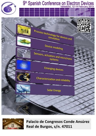
  • 3. 


 CDE’2013
 
 9th
Spanish
Conference
 On
Electron
Devices
 
 Palacio
de
Congresos
 Conde
Ansúrez
 
 Valladolid,
Spain
 February
12‐14,

2013
 
 www.cde2013.es


  • 4.
  • 5. 
 
 
 COMMITTEES
 
 LOCAL
COMMITTEE
 
 Luis
Alberto
Bailón
Vega
 Dpt.

Electricidad
y
Electrónica,
UVa
 Ismael
Barba
García
 Dpt.

Electricidad
y
Electrónica,
UVa
 Helena
Castán
Lanaspa
 (chair)
 Dpt.

Electricidad
y
Electrónica,
UVa
 Salvador
Dueñas
Carazo
 Dpt.

Electricidad
y
Electrónica,
UVa
 Héctor
García
García
 (papers)
 Dpt.

Electricidad
y
Electrónica,
UVa
 Miguel
Ángel
González
Rebollo
 Dpt.
Física
de
la
Materia
Condensada,
Cristalografía
y
Mineralogía,
UVa
 Ana
Grande
Sáez
 Dpt.

Electricidad
y
Electrónica,
UVa
 Juan
Jiménez
López
 Dpt.
Física
de
la
Materia
Condensada,
Cristalografía
y
Mineralogía,
UVa
 Ana
Cristina
López
Cabeceira
 Dpt.

Electricidad
y
Electrónica,
UVa
 Luis
Alberto
Marqués
Cuesta
 Dpt.

Electricidad
y
Electrónica,
UVa
 José
Represa
Fernández
 Dpt.

Electricidad
y
Electrónica,
UVa
 
 
 i

  • 6. 
 ADVISORY
COMMITTEE
 José
Millán
‐
IMB‐CNM‐CSIC

 (CDE
Advisory
Committee
Chair)
 Juan
A.
de
Agapito
‐
Universidad
Complutense
de
Madrid
 Xavier
Aymerich
‐
Universidad
Autónoma
de
Barcelona
 Luis
Bailón
‐
Universidad
de
Valladolid
 Fernando
Briones
‐
IMM‐CNM‐CSIC
 Enrique
Calleja
‐
Universidad
Politécnica
de
Madrid
/
ISOM
 Pedro
Cartujo
‐
Universidad
de
Granada
 Luis
Castañer
‐
Universidad
Politécnica
de
Cataluña
 Xavier
Correig
‐
Universidad
Rovira
i
Virgili
 Eugenio
García
Moreno
‐
Universidad
de
las
Islas
Baleares
 Javier
Gracia
‐
CEIT
 F.
Javier
Gutiérrez
Monreal
‐
IFA‐CSIC
 Antonio
Luque
‐
Universidad
Politécnica
de
Madrid
/
IES
 Joan
Ramón
Morante
‐
Universidad
de
Barcelona
/
IREC
 Elías
Muñoz
Merino
‐
Universidad
Politécnica
de
Madrid
/
ISOM
 Daniel
Pardo
‐
Universidad
de
Salamanca
 Juan
Piqueras
‐
Universidad
Autónoma
de
Madrid
 Francisco
Serra
‐
Universidad
Autónoma
de
Barcelona
/
CNM‐CSIC
 TECHNICAL
COMMITTEE
 Antonio
García
Loureiro
‐
Universidad
de
Santiago
de
Compostela
 Ramón
Alcubilla
‐
Universidad
Politécnica
de
Catalunya
 Carlos
Algora
‐
Universidad
Politécnica
de
Madrid
/
IES
 Angel
Luis
Alvarez
Castillo
‐
Universidad
Rey
Juan
Carlos
 Javier
Berganzo
‐
IKERLAN
 Carles
Cané
‐
IMB‐CNM‐CSIC
 Fernando
Calle
‐
Universidad
Politécnica
de
Madrid
/
ISOM
 Enrique
Castaño
‐
CEIT
 Salvador
Dueñas
Carazo
‐
Universidad
de
Valladolid
 Ignacio
Garcés
‐
Universidad
de
Zaragoza
 Tomás
González
‐
Universidad
de
Salamanca
 María
Jesús
Hernández
‐
Universidad
Autónoma
de
Madrid
 Carmen
Horrillo
‐
IFA‐CSIC
 Pedro
Ibañez
Ereño
‐
ROBOTIKER
 Fernando
López
‐
Universidad
Carlos
III
 Juan
A.
López
Villanueva
‐
Universidad
de
Granada
 Lluis
Marsal
‐
Universidad
Rovira
i
Virgili
 Ignacio
Mártil
de
la
Plaza
‐
Universidad
Complutense
de
Madrid
 Enrique
Maset
‐
Universidad
de
Valencia
 Montserrat
Nafria
‐
Universidad
Autónoma
de
Barcelona
 Isabel
Obieta
Villalonga
‐
INASMET
 Rodrigo
Picos
‐
Universidad
de
las
Islas
Baleares
 José
Manuel
Quero
Reboul
‐
Universidad
de
Sevilla
/
AICIA
 José
María
Ripalda
Cobian
‐
IMM‐CNM‐CSIC
 Albert
Romano
Rodríguez
‐
Universidad
de
Barcelona
 ii
 

  • 7. SUPPORTED
BY:


 TECHNICAL
CO‐SPONSORSHIP:


 iii

  • 8. 
 
 
 iv
 

  • 9. 


 WELCOME
LETTER
 
 The
 9th
 Spanish
 Conference
 on
 Electron
 Devices
 brings
 together
 the
 work
 of
 both
 research
groups
and
companies
on
the
field
of
electronic
devices.
This
edition
will
take
 place
 from
 the
 12th

 to
 the
 14th
 of
 February
 of
 2013,
 in
 Valladolid,
 carrying
 on
 with
 a
 series
of
previous
events
in
Palma
de
Mallorca
(2011),
Santiago
de
Compostela
(2009),
 El
 Escorial
 (Madrid,
 2007),
 Tarragona
 (2005),
 Calella
 de
 la
 Costa
 (2003),
 Granada
 (2001),
Madrid
(1999)
and
Barcelona
(1997).
 As
usual,
the
Conference
program
consists
of
invited
and
contributed
papers
organized
 in
the
topic
sessions.
The
Congress
will
conclude
with
a
workshop
about
Solar
Energy,
 which
will
be
composed
by
7
talks,
22
posters
and
a
round
table
with
the
participation
 of
companies
from
the
Solar
Energy
Cluster
of
Castilla
and
León.

Just
before
the
CDE
 conference
opening,
a
Mini
Colloquium
(MQ)
of
Electron
Device
Society
(EDS)
will
take
 place
at
the
same
venue
as
CDE,
without
additional
registration
fees.
In
this
way,
all
the
 CDE
participants
may
attend
to
both
events.
 
 The
 total
 number
 of
 contributions
 is
 122:
 2
 plenary
 talks,
 11
 invited
 talks,
 25
 talks,
and
84
posters,
distributed
in
the
following
topics:
 S1
 Process
technology
for
devices
and
simulation
 S2
 Device
modeling
 S3
 Sensors,
actuators
and
micro/nano
systems
 S4
 Emerging
devices
 S5
 Characterization
and
reliability
 S6
 Solar
energy:
thermal
and
photovoltaic
devices
 
 Most
of
the
contributions
presented
at
this
conference
come
from
Spanish
Universities
 and
Research
Centers.
30
%
of
them
are
fruit
of
the
cooperation
between
Spanish
and
 foreigner
 institutions
 and
 15%
 of
 the
 works
 come
 from
 researchers
 of
 foreign
 countries.
 It
 is
 important
 to
 point
 out
 the
 high
 number
 of
 collaborations
 among
 different
 institutions
 (41%),
 so
 indicating
 the
 increase
 of
 cooperative
 work
 of
 the
 Spanish
research
groups
in
the
CDE
scope.


 Because
 of
 the
 delicate
 economic
 situation,
 fundings
 to
 the
 Congress
 have
 been
 significantly
 reduced
 compared
 to
 previous
 years,
 so
 this
 issue
 will
 necessarily
 be
 austere
 without
 any
 impact
 on
 the
 scientific
 quality.
 We
 appreciate
 in
 advance
 the
 understanding
 of
 this
 forced
 sobriety
 and
 we
 are
 convinced
 that
 in
 order
 to
 address
 these
difficulties
we
must
use
all
our
resources
to
ensure
that
science
and
progress
will
 continue
developing.


 v

  • 10. As
Vladimir
Nabokov
says:
“there
is
no
science
without
fancy”,
although
Hans
Magnus
 Enzensberger
 believes
 that
 "poetry
 of
 science
 is
 not
 at
 ground
 level,
 but
 comes
 from
 the
 deepest
 layers".
 We
 have
 organized
 this
 conference
 with
 the
 belief
 that
 scientific
 research
is
a
great
privilege
for
the
human
being.
 
 We
would
like
to
thank
all
the
supports
received
from
the
following
organizations
and
 companies:
The
University
of
Valladolid,
the
Government
of
Castilla
y
León,
the
City
of
 Valladolid,
the
IEEE
Spanish
Section,
and
Instrumentos
de
Medida
S.L.
We
extend
our
 thanks
to
the
CDE
Advisory
and
Technical
Committees,
as
well
as
to
the
organizers
of
 the
CDE
from
previous
editions.
 Our
very
special
thank
to
the
CDE
Advisory
Committee
Chair,
Prof.
José
Millán.
 
 The
Conference
Local
Committee
 Contribu)ons
from
Spanish
Research
 Centers
and
Universi)es
 16
 14
 12
 10
 8
 6
 4
 2
 0
 Contribu)ons
form
Foreign
Countries
 8
 6
 4
 2
 0
 vi
 

  • 11. 
 
 CDE
2013


PROGRAM
 Tuesday,
Feb.
12,
2013
 14.00
h
‐

20.00
h
 REGISTRATION
 14.00
h
–
18.00
h

 Mini
 Colloquium
 EDS.
 Prof.
 Benjamín
 Íñiguez,
 Univ.
 Rovira
 I
 Virgili,
Chair
 18.30
h
–
20.00
h

 WELCOME
RECEPTION

 20.00
h
‐

 
 RUTA
DE
TAPAS
 
 Wednesday,
Feb.
13,
2013
 8.00
h
–
8.30
h

 REGISTRATION
 8.30
h
–
8.45
h

 OPENING:
Prof.
José
Millán,
CDE
Advisory
Committee
Chair
 8.45

h
–
9.30
h

 PLENARY
TALK:
Prof.
Emilio
Lora‐Tamayo,
CSIC
Chair
 9.30
h
‐
11.35
h

 SESSION
1:
Process
technology
for
devices
and
simulation
 11.35
h
–
12.00
h
 COFFEE
BREAK
 12.00
h
–
14.05
h

 SESSION
2:
Device
modeling
 14.05
h
–
15.30
h
 LUNCH
 15.30
h
–
17.35
h
 SESSION
3:
Sensors,
actuators
and
micro/nano
systems
 17.35
h
–
18.00
h
 COFFEE
BREAK
 
 
 CDE
Advisory
Committee
Meeting
 18.00
h
–
19.30
h

 POSTER:
SESSIONS
1
‐
5
 19.30
h
‐

20.30
h
 CLASSICAL
MUSIC
PERFORMANCE
 21.30
h
‐

 
 GALA
DINNER

 EDS
Chapter
of
the
Year
Award
 
 Award
 Thursday,
Feb.
14,
2013
 8.00
h
–
10.05
h

 SESSION
4:
Emerging
devices
 
 10.05
h
‐
10.30
h

 COFFEE
BREAK
 10.30
h
–
12.35
h
 SESSION
5:
Characterization
and
reliability
 
 12.35
h
‐
 
 WORKSHOP:
SOLAR
ENERGY
 12.35
h
–
14.00
h

 POSTER:
SESSION
6
 14.00
h
–
15.30
h
 LUNCH
 
 15.30
h
–
16.15
h
 PLENARY
TALK:
Prof.
Carlos
Algora,
IES‐UPM
 
 16.15
h
–
18.15
h
 SESSION
6:
Solar
Energy:
thermal
and
photovoltaic
devices
 
 18.15
h
–
18.30
h
 COFFEE
BREAK
 
 18.30
h
–
19.45
h

 ROUND
TABLE.
Prof.
Juan
Jiménez,
Univ.
Valladolid.
Chair
 
 19.45
h
–
20.00
h

 CLOSING
REMARKS
 
 EDS:
Best
Student
Award


 OUT
OF
PROGRAM:
 Friday,
Feb.
15,
2013


(for
the
participants
staying
in
Valladolid)
 Sightseeing
on
foot
and
museums.
 
 CDE2013
 1
 

  • 12. Tuesday,
Feb.
12,
2013
 14.00
h
‐

20.00
h
 Palacio
de
Congresos
Conde
Ansúrez,
third
floor
 REGISTRATION
 
 14.00
h
–
18.00
h

 Auditorium,
Palacio
de
Congresos
Conde
Ansúrez,
third
floor
 EDS
MINI
COLLOQUIUM.
Prof.
Benjamín
Íñiguez,
Univ.
Rovira
I
 Virgili.
Chair
 
 18.30
h
–
20.00
h

 Palacio
de
Santa
Cruz
 WELCOME
 RECEPTION:
 Prof.
 Marcos
 Sacristán,
 Chancellor
 of
 
 University
of
Valladolid
 
 20.00
h
‐

 
 RUTA
DE
TAPAS:
Tapas
bars
in
the
city
center
 
 Wednesday,
Feb.
13,
2013
 
 8.00
h
–
8.30
h

 Palacio
de
Congresos
Conde
Ansúrez,
third
floor
 REGISTRATION
 8.30
h
–
8.45
h

 Auditorium,
Palacio
de
Congresos
Conde
Ansúrez,
third
floor
 OPENING:
Prof.
José
Millán,
CDE
Advisory
Committee
Chair
 9.30
h
‐
11.35
h

 Auditorium,
Palacio
de
Congresos
Conde
Ansúrez,
third
floor
 SESSION
 1:
 Process
 technology
 for
 devices
 and
 simulation
 Chairperson:
Prof.
Javier
Martínez
Rodrigo
 
 9.30
h
–
9.55
h
 O.1.1.
 Invited:
 Thin
Dielectric
Films
Grown
by
Atomic
Layer
Deposition:
Properties
 and
Applications.
 Francesca
Campabadal,
J.M.
Rafí,
M.B.
González,
M.Zabala,
O.
Beldarrain,
M.C.
Acero
 and
M.
Duch
 Institut
de
Microelectrònica
de
Barcelona,
IMB‐CNM
(CSIC).

 
 9.55
h
–
10.15
h
 O.1.2.
 Plasma
 oxidation
 of
 metallic
 Gd
 deposited
 on
 silicon
 by
 high
 pressure
 sputtering
as
high
permittivity
dielectric


 R38
 M.
A.
Pampillón1,
P.
C.
Feijoo1,
E.
San
Andrés1,
J.
L.
G.
Fierro2
 1
 Departamento
 de
 Física
 Aplicada
 III
 (Electricidad
 y
 Electrónica).
 Facultad
 de
 Ciencias
Físicas.
Universidad
Complutense
de
Madrid.
28040,
Madrid,
Spain.

 2
Instituto
de
Catálisis
y
Petroleoquímica.
CSIC.
Cantoblanco.
28049,
Madrid,
Spain.
 2
 PROGRAMA
 

  • 13. 10.15
h
–
10.35
h
 O.1.3.
Use
of
PMMA
to
obtain
Graphene
layers


 R93
 A.
 Bosca 1,
 
 D.
 Lopez‐Romero1,
 S.
 Alvarez‐Garcia2,
 A.
 de
 Andres2,
 J.
 Pedros1,
 J.
 Martinez1
and
F.
Calle1
 1
Instituto
de
Sistemas
Optoelectrónicos
y
Microtecnología,
Universidad
Politécnica
 de
Madrid,
28040
Madrid,
Spain.
 2
Instituto
de
Ciencia
de
Materiales
de
Madrid,
Consejo
Superior
de
Investigaciones
 Científicas,
28049
Madrid,
Spain.
 
 10.35
h
–
10.55
h
 O.1.4.
Nanodevice
simulations
on
CloudStack


 R98
 F.
Gomez‐Folgar,
E.
Comesaña,
R.
Valin,
A.
Garcia‐Loureiro,
T.
F.
Pena.
 Centro
 de
 Investigación
 en
 Tecnoloxías
 da
 Información
 (CITIUS).
 Universidad
 de
 Santiago
de
Compostela.
 
 10.55
h
–
11.15
h
 O.1.5.
 Direct‐write
 patterning
 of
 metals
 and
 reduced
 graphene
 oxide
 electrodes
 by
 arc
erosion
for
organic
device
manufacturing


 R110
 M.
 García‐Vélez,
 A.
 L.
 Alvarez,
 C.
 Coya,
 G.
 Alvarado,
 J.
 Jiménez‐Trillo1,
 X.
 Diéz‐ Betriú2,
A.
de
Andrés2
 Dpt.
Tecnología
Electrónica,
ESCET,
Universidad
Rey
Juan
Carlos,
Móstoles,
28933
 Madrid
(Spain)
 1Dpt.
 Ingeniería
 de
 Circuitos
 y
 Sistemas,
 EUIT
 Telecomunicación,
 UPM,
 28031
 Madrid
(Spain)
 2Instituto
 de
 Ciencia
 de
 Materiales
 de
 Madrid,
 CSIC.
 Cantoblanco,
 28049
 Madrid
 (Spain)
 
 11.15
h
–
11.35
h
 O.1.6.

Microscopic
modeling
of
interdiffusion
in
SiGe
alloys
 
 R117
 Pedro
Castrillo,
Iván
Santos,
Ruth
Pinacho,
Emiliano
Rubio,
and
Martín
Jaraiz
 Dpto.
 de
 Electrónica,
 Universidad
 de
 Valladolid,
 E.T.S.I.
 Telecomunicación,
 Paseo
 Belén
15,
47011
Valladolid,
Spain.
 
 11.35
h
–
12.00
h
 COFFEE
BREAK
 
 12.00
h
–
14.05
h

 Auditorium,
Palacio
de
Congresos
Conde
Ansúrez,
third
floor
 SESSION
2:
Device
modeling
 Chairperson:
Prof.
Juan
Antonio
López
Villanueva
 
 12.00
h
–
12.25
h
 O.2.1.
Invited:
Modeling
of
radiation
effects
in
MOSFETs
 Jesús
Banqueri,
M.
A.
Carvajal
and
A.
J.
Palma
 ECsens
(Electronic
and
Chemical
SENsing
Solutions),
Departamento
de
Electrónica
 y
Tecnología
de
Computadores.
Universidad
de
Granada.

 CDE2013
 3
 

  • 14. 
 12.25
h
–
12.45
h
 O.2.2.
 A
 new
 strategy
 to
 improve
 frequency
 performance
 of
 emerging
 devices
 without
length
scaling


 R116
 A.
Benali,
F.
L.
Traversa,
G.
Albareda,
M.
Aghoutaneb 1
and
X.
Oriols

 Universitat
Autònoma
de
Barcelona,
08193,
Bellaterra,
Spain

 1Universidad
Abdelmalek
Essaâdi,
93000,
Tetuán,
Morocco
 
 12.45
h
–
13.05
h
 O.2.3.
 Wide
 frequency
 band
 scalable
 modeling
 of
 3D
 embedded
 decoupling
 capacitors
 Hélène
Jacquinot1,
David
Denis2


 R22
 1CEA,
LETI,
MINATEC
Campus,
17
rue
des
Martyrs,
38054
Grenoble.
France.
 2IPDIA,
2
rue
de
la
Girafe,
14000
Caen.
France.
 
 13.05
h
–
13.25
h
 O.2.4.
Monte
Carlo
analysis
of
thermal
effects
in
Self‐Switching
Diodes
 
 R48
 J.‐F.
Millithaler,
I.
Iñiguez‐de‐la‐Torre,
T.
González,
J.
Mateos

 Departamento
 de
 Física
 Aplicada,
 Universidad
 de
 Salamanca,
 37008
 Salamanca,
 Spain.
 
 13.25
h
–
13.45
h
 O.2.5.
OTFT
modeling:
development
and
implementation
in
EDA
tools
 
 R113
 A.
Castro‐Carranza 1,
M.
Cheralathan1,
C.
Valla2,
M.
Estrada3,
A.
Cerdeira3,
F.
Poullet2,
 G.
Depeyrot2,
B.
Iñiguez1
and
J.
Pallarès1
 1Departament
 d’Enginyeria
 Electrònica
 (DEEEA),
 
 Universitat
 Rovira
 I
 Virgili
 43007,
Tarragona,
Spain.

 2DOLPHIN
Integration
GmbH,
F‐38242
Meylan,
France.
 3Sección
 de
 Electrónica
 del
 Estado
 Sólido
 (SEES),
 CINVESTAV‐IPN,
 07360
 Mexico
 D.F.,
Mexico.
 
 13.45
h
–
14.05
h
 O.2.6.

Analysis
of
Crossover
Point
and
Threshold
Voltage
for
Triple
Gate
MOSFET.

 Dheeraj
Sharma
and
Santosh
Vishvakarma


 R62
 Nanoscale
Devices,
VLSI/Circuit
and
System
Design
Lab,
Electrical
Engineering,

 Indian
Institute
of
Technology,
Indore,
India.
 
 14.05
h
–
15.30
h
 LUNCH


 4
 PROGRAMA
 

  • 15. 15.30
h
–
17.35
h
 Auditorium,
Palacio
de
Congresos
Conde
Ansúrez,
third
floor
 SESSION
3:
Sensors,
actuators
and
micro/nano
systems
 Chairperson:
Prof.
Carmen
Horrillo
 15.30
h
–
15.55
h
 O.3.1.
Invited:
Sensors
and
Microsytems
for
the
Food
sector.

 Carles
Cané.
 Institut
de
Microelectrònica
de
Barcelona,
IMB‐CNM
(CSIC).

 
 15.55
h
–
16.15
h
 O.3.2.
Benzene
sensor
based
on
in‐situ
grown
ZnO
nanostructures
 
 R47
 J.
Gonzalez‐Chavarri,
I.
Castro‐Hurtado,
G.
G.
Mandayo,
and
E.
Castaño

 Ceit
and
Tecnun,
P.
Manuel
Lardizabal
15,
20018,
San
Sebastian,
Spain
 
 16.15
h
–
16.35
h
 O.3.3.
Ceramic
Capacitive
Pressure
Sensor
based
on
LTCC
Technology


R65
 Josep
 M.
 Fernández‐Sanjuán1,2,
 Núria
 Bonet2,
 Josep
 G.
 Rodríguez2,
 Francisco
 M.
 Ramos1,2,
Javier
J.
Sieiro3,
José
M.
López‐Villegas3,
Albert
Cirera1
 1MIND/IN2UB
Electronics
Department,
Universitat
de
Barcelona,
Martí
i
Franquès,
 1,
Barcelona
08028,
Spain.
 2FAE‐
Francisco
Albero
S.A.U.,
Rafael
Barradas
19,
L’Hospitalet
de
Llobregat
08908,
 Spain.
 3GRAF
 Electronics
 Department,
 Universitat
 de
 Barcelona,
 Martí
 i
 Franquès,
 1,
 Barcelona
08028,
Spain.
 16.35
h
–
16.55
h
 O.3.4.
Microfluidics
applied
to
Love‐wave
devices
to
detect
biological
warfare
agents
 in
dynamic
mode.


 R67
 D.
 Matatagui1,
 J.
 Fontecha1,
 M.J.
 Fernández1,
 I.
 Gràcia2,
 C.
 Cané2,
 J.P.
 Santos1,
 M.C.
 Horrillo1

 1GRIDSEN,
CSIC,
Serrano
144,
28006
Madrid,
Spain
 2Instituto
de
Microelectrónica
de
Barcelona,
CSIC,
Campus
UAB,
08193
Bellaterra,
 Spain
 
 16.55
h
–
17.15
h
 O.3.5.
Electroosmotic
impulsion
device
for
integration
in
PCB‐MEMS


R96
 Antonio
Luque,
José
M.
Soto,
Francisco
Perdigones,
Carmen
Aracil,
José
M.
Quero.
 Dpto.
 Ingeniería
 Electrónica,
 Escuela
 Técnica
 Superior
 de
 Ingeniería,
 Universidad
 de
Sevilla.
Av.
Descubrimientos
s/n

E41092
Sevilla.
 
 17.15
h
–
17.35
h
 O.3.6.
 Low
 power
 consumption
 single
 metal
 oxide
 nanowire
 based
 gas
 sensor
 integrated
on
MEMS
Microhotplates


 R104
 J.
 Samà1,
 R.
 Jiménez‐Díaz1,
 J.D.
 Prades1,
 O.
 Casals1,
 F.
 Hernandez‐Ramirez2
 3,
 J.
 Santander4,
C.
Calaza4,

L.
Fonseca4,
C.
Cané4,
S.
Barth5,
A.
Romano‐Rodríguez1
 CDE2013
 5
 

  • 16. 1
 MIND‐IN2UB‐Dept.
 Electronics,
 Universitat
 de
 Barcelona
 (UB),
 Martí
 i
 Franquès
 1,
08028,
Barcelona,
Spain.

 2
 Institut
 de
 Recerca
 en
 Energia
 de
 Catalunya,
 Jardins
 de
 les
 Dones
 de
 Negre
 1,
 08930
Sant
Adrià
de
Besòs,
Spain

 3
 Dept.
 Electronics,
 Universitat
 de
 Barcelona
 (UB),
 Martí
 i
 Franquès
 1,
 08028,
 Barcelona,
Spain
 4
 Institut
 
 de
 Microelectrònica
 de
 Barcelona,
 IMB‐CNM‐CSIC,
 08193
 Bellaterra,
 Spain
 5
Institute
of
Materials
Chemistry,
TU
Wien,
Getreidemarkt
9/165,
A‐1060
Vienna,
 Austria.
 
 17.35
h
–
18.00
h
 COFFEE
BREAK
 18.00
h
–
19.30
h

 Palacio
de
Congresos
Conde
Ansúrez,
second
floor
 POSTER:
SESSIONS
1
‐
5
 
 POSTER
‐
SESSION
1:
Process
technology
for
devices
and
simulation
 P.1.1.
Gadolinium
scandate
by
high
pressure
sputtering
as
a
high‐k
dielectric


R5
 P.C.
Feijoo,
M.A.
Pampillón,
E.
San
Andrés
 Dpto.
 Física
 Aplicada
 III:
 Electricidad
 y
 Electrónica.
 Universidad
 Complutense
 de
 Madrdid.
Av/Complutense
S/N.
28040
Madrid
(Spain).
 
 P.1.2.
Effects
of
Ozone
Pre‐deposition
Treatment
on
GaSb
MOS
Capacitors


R13
 Zhen
Tan,
Lianfeng
Zhao,
Ning
Cui,
Jing
Wang,
and
Jun
Xu
 Tsinghua
National
Laboratory
for
Information
Science
and
Technology,
Institute
of
 Microelectronics,
Tsinghua
University,
Beijing
100084,
P.R.China.

 
 P.1.3.
 Towards
 high‐k
 integration
 with
 III‐V
 channels:
 interface
 optimization
 of
 high
pressure
sputtered
Gd2O3
on
InP


R45
 E.
San
Andrés,
M.
A.
Pampillón,
C.
Cañadilla,
P.
C.
Feijoo,
A.
del
Prado.
 Departamento
 de
 Física
 Aplicada
 III
 (Electricidad
 y
 electrónica).
 Facultad
 de
 Ciencias
Físicas,
Universidad
Complutense
de
Madrid.
Madrid,
E‐28040.
 
 P.1.4.
Etching
of
AlGaN/GaN
HEMT
structures
by
Cl2‐based
ICP


R55
 Z.
Gao,
M.
F.
Romero,
F.
Calle
 Dpto.
 Ingeniería
 Electrónica
 and
 Instituto
 de
 Sistemas
 Optoelectrónicos
 y
 Microtecnología.
 ETSI
 Telecomunicación,
 Universidad
 Politécnica
 de
 Madrid,
 28040
Madrid,
Spain.
 
 P.1.5.
Ab
initio
study
of
the
electronic
properties
of
defect
states
in
Silicon


R94
 Iván
Santos,
María
Aboy,
Pedro
Castrillo,
Pedro
López,
Lourdes
Pelaz,
and
Luis
A.
 Marqués.
 6
 PROGRAMA
 

  • 17. Dpto.
 de
 Electrónica,
 Universidad
 de
 Valladolid,
 E.T.S.I.
 Telecomunicación,
 Paseo
 Belén
15,
47011
Valladolid,
Spain.
 
 P.1.6.
 Two
dimensional
electron
gas
related
luminescence
in
InAl(Ga)N/AlN/GaN‐ based
heterostructures


R106
 M.
 F.
 Romero 1,
 M.
 Feneberg2,
 A.
 Minj3,
 A.
 Cavallini3,
 P.
 Gamarra4,
 M.‐A.
 di
 Forte
 Poisson4,
A.
Vilalta‐Clemente5,
P.
Ruterana5,
F.
Calle1,
and
R.
Goldhahn2,6

 1ISOM,
 ETSI
 Telecomunicación,
 Universidad
 Politécnica
 de
 Madrid,
 Av.
 Complutense
30,
28040
Madrid,
Spain

 2Institut
 für
 Experimentelle
 Physik,
 Otto‐von‐Guericke‐Universität
 Magdeburg,
 39106
Magdeburg,
Germany

 3Department
 of
 Physics,
 University
 of
 Bologna,
 viale
 C
 Berti
 Pichat
 6/II,
 I‐40127
 Bologna,
Italy

 4III‐V
Lab.,
Route
de
Nozay,
91461
Marcoussis,
France

 5CIMAP,
 UMR
 6252
 CNRS‐ENSICAEN‐CEA‐UCBN,
 6,
 Boulevard
 du
 Maréchal
 Juin,
 14050
Caen
Cedex,
France

 6Institut
 für
 Physik,
 Technische
 Universität
 Ilmenau,
 PF100565,
 98684
 Ilmenau,
 Germany.
 
 P.1.7.
 Fabrication
 of
 High‐Ordered
 PBDTTT‐CF
 Polymer
 Nanopillar
 Arrays
 for
 Optoelectronic
Applications


 R109
 V.S.
Balderrama,
J.
Ferré‐Borrull,
J.
Pallarés,
and
L.F.
Marsal
 Departament
d’Enginyeria
Electrònica,
Elèctrica
i
Automàtica,
Universitat
Rovira
i
 Virgili,
Avda.
Països
Catalans
26,
43007
Tarragona,
Spain.
 
 P.1.8.
Identification
of
stable
defect
structures
induced
by
irradiation
in
Si


R112
 Pedro
López,
Lourdes
Pelaz,
Luis
A.
Marqués,
Iván
Santos
and
María
Aboy
 Departamento
 de
 Electricidad
 y
 Electrónica,
 Universidad
 de
 Valladolid,
 ETSI
 Telecomunicación,
Paseo
de
Belén
15,
47011
Valladolid,
Spain.
 
 P.1.9.
 Photonic
 crystal
 optimization
 using
 a
 process
 variation
 aware
 genetic
 algorithm.


 R120
 Rodrigo
Picos 1,
Bernat
Mut1,
Eugeni
Garcia‐Moreno1,
Lluis
F.
Marsal2

 1Universitat
de
les
Illes
Balears,
GEE,
Illes
Balears,
Spain.
 2Universitat
Rovira
i
Virgili,
DEEA,
Tarragona,
Spain.
 
 POSTER
‐
SESSION
2:
Device
modeling
 
 P.2.1.
Subthreshold
response
of
a
MOSFET
to
radiation
effects


 R3
 A.J.
 Palma1,
 M.A.
 Carvajal1,
 S.
 Martínez‐García1,
 M.
 Vilches2,
 A.M.
 Lallena 3
 and
 J.
 Banqueri 1
 1Electronics
Department,
ETSIIT.
 CDE2013
 7
 

  • 18. 3Atomic,
Nuclear
and
Molecular
Physics
Department,
Science
Faculty,
University
of
 Granada.
 2Universitary
Hospital
“San
Cecilio”
Granada
(Spain).
 
 P.2.2.
 Effects
of
Coverage
Factor,
Inhomogeneous
Broadening
and
Cavity
Length
on
 Static
and
Dynamic
Behavior
of
Self‐Assembled
Quantum‐Dot
Lasers
 
 R16
 Mahdi
Razm‐Pa 1,
and
Farzin
Emami2
 1Electronic
 Department,
 Islamic
 Azad
 University,
 Boushehr
 Branch
 Islamic
 Azad
 University
of
Boushehr,
Boushehr,
Iran.
 2Optoelectronic
 Research
 Centre
 of
 Electronic
 Department,
 Shiraz
 University
 of
 Technology,
Airport
Blvd.,
Shiraz,
Iran.


 P.2.3.
 Space
 quantization
 effects
 in
 Double
 Gate
 SB‐MOSFETs:
 role
 of
 the
 active
 layer
thickness


 R20
 José
S.
García,
María
J.
Martín,
Raúl
Rengel
 Departamento
 de
 Física
 Aplicada.
 Universidad
 de
 Salamanca.
 Plaza
 de
 La
 Merced
 s/n.
37008.
Salamanca.
Spain.
 
 P.2.4.
 Schottky
Barrier
MOSFETs
working
in
the
linear
regime:
A
Monte
Carlo
study
 of
microscopic
transport.


 R21
 Carlos
Couso,
Raúl
Rengel
and
María
J.
Martín
 Departamento
de
Física
Aplicada,
Universidad
de
Salamanca,
Spain.
 
 P.2.5.
 A
 simple
 compact
 model
 for
 the
 junctionless
 Variable
 Barrier
 Transistor
 (VBT).


 R27
 Oana
Moldovan,
Francois
Lime,
Bogdan
Nae,
Benjamin
Íñiguez.
 Universitat
Rovira
i
Virgili
(URV),
ETSE
DEEEA.
Tarragona,
Spain.
 
 P.2.6.
 Influence
of
the
Contact
Effects
on
the
Variation
of
the
Trapped
Charge
in
the
 Intrinsic
Channel
of
OTFTs


 R33
 KM
Awawdeh 1,
JA
Jiménez
Tejada1,
P
López
Varo1,
JA
López
Villanueva1,
MJ
Deen2
 1Departamento
de
Electrónica
y
Tecnología
de
Computadores.
CITIC‐UGR.
Facultad
 de
Ciencias.
Universidad
de
Granada.
18071
Granada,
SPAIN.
 2Department
 of
 Electrical
 and
 Computer
 Engineering
 McMaster
 University,
 Hamilton,
ON
L8S
4K1
CANADA.
 P.2.7.
 An
 Improved
 I‐V
 Model
 of
 4H‐SiC
 MESFETs
 Incorporating
 Substrate
 Trapping,
Surface
Trapping
and
Thermal
Effects


 R39
 M.
Hema
Lata
Rao, 

Student
Member
IEEE
and
Neti
V.L.Narasimha
Murty
 School
of
Electrical
Sciences,
IIT
Bhubaneswar,
India.
 
 P.2.8.
 Time‐domain
 Monte
 Carlo
 simulations
 of
 resonant‐circuit
 operation
 of
 GaN
 Gunn
diodes


 R43
 8
 PROGRAMA
 

  • 19. S.
García,
B.
G.
Vasallo,
J.
Mateos
and
T.
González

 Departamento
 de
 Física
 Aplicada,
 Universidad
 de
 Salamanca,
 Plaza
 de
 la
 Merced
 s/n,
37008
Salamanca,
Spain.
 
 P.2.9.
Study
of
RFIDs
with
SOI
technology
for
UWB


 R49
 Raúl
 Rodríguez1,
 B.
 González1,2,
 J.
 García1,2,
 M.
 Marrero‐Martín 1,2,
 and
 A.
 Hernández 1,2
 1
Institute
for
Applied
Microelectronics
(IUMA).
Universidad
de
Las
Palmas
de
Gran
 Canaria
(ULPGC)
 2Departamento
de
Ingeniería
Electrónica
y
Automática.
Universidad
de
Las
Palmas
 de
Gran
Canaria
(ULPGC)
 
 P.2.10.
 Performance
 of
 Two
 Possible
 Implementations
 of
 ILUT
 Preconditioners
 in
 the
3D
Nanodevice
Simulation


 R54
 A.
Garcia–Rivera1,
R.Valin1,
N.
Seoane1,
M.
Aldegunde2,
and
A.
J.
Garcia–Loureiro1
 1Centro
 Singular
 de
 Investigación
 en
 Tecnoloxías
 da
 Información
 (CITIUS),
 Rúa
 Jenaro
 de
 la
 Fuente
 Domínguez
 s/n,
 Universidade
 de
 Santiago
 de
 Compostela
 (USC)
–
Campus
Vida,
15782
–
Santiago
de
Compostela,
España.
 2College
of
Engineering,
Swansea
University
–
Swansea,
United
Kingdom

 
 P.2.11.
 Static
 and
 Dynamic
 Characteristics
 of
 Self‐Assembled
 InAs‐GaAs
 Quantum
 Dot
 Laser
 Considering
 Carrier
 Recombination
 and
 Escape
 Time;
 A
 Circuit‐Level
 Modeling


 R15
 Mahdi
Razm‐Pa 1,
and
Farzin
Emami2


 1Electronic
Department,
Islamic
Azad
University,
Boushehr
Branch,
Iran.
 2Optoelectronic
Research
Centre
of
Electronic
Department,
Shiraz
University
of
 Technology.

Airport
Blvd.,
Shiraz,
Iran.


 P.2.12.
Macroporous
Silicon
FET
Transistors
for
Power
Applications
 
 R69
 Didac
Vega,
Raúl
Najar,
María
Pina,
Ángel
Rodríguez
 Departament
de
Enginyeria
Electronica.
Universitat
Politècnica
de
Catalunya
(UPC)
 Spain
 
 P.2.13.
 Study
of
statistical
variability
in
22
nm
SOI
FinFET
introduced
by
LER,
RDF
 and
MGG


 R102
 G.
Indalecio 1,
A.
García‐Loureiro1
,
M.
Aldegunde2,
K.Kalna2
 1Dpt.
 De
 Electrónica
 y
 Computación,
 Universidad
 de
 Santiago
 de
 Compostela,
 Spain.
 2College
of
Engineering,
Swansea
University,
Swansea
SA2
8PP,
United
Kingdom


 CDE2013
 9
 

  • 20. POSTER
‐
SESSION
3:
Sensors,
actuators
and
micro/nano
systems
 
 P.3.1.
 SENSOSOL:
 MultiFOV
 4‐Quadrant
 high
 precision
 sun
 sensor
 for
 satellite
 attitude
control


 R11
 Francisco
 J.
 Delgado1,
 José
 M.
 Quero1,
 Juan
 García1,
 Cristina
 L.
 Tarrida1,
 José
 M.
 Moreno1,
Agustín
G.
Sáez1,
Pablo
Ortega2
 1Escuela
 Superior
 de
 Ingenieros,
 Universidad
 de
 Sevilla
 (US,
 Spain),
 fjdelgado@gte.esi.us.es.

 2Universidad
 Politécnica
 de
 Cataluña,
 Grupo
 de
 Micro
 y
 Nanotecnologías
 (UPC,
 Spain)
 P.3.2.
Carbon
Nanotube‐based
SAW
sensors


 R25
 I
Sayago1,
M
J
Fernández1,
J
L
Fontecha1,
M
C
Horrillo1,
E
Terrado2,
A
Seral‐Ascaso3
 and
E
Muñoz3
 1
Instituto
de
Seguridad
de
la
Información

(GRIDSEN)‐
CSIC,
Serrano
144,
28006
 Madrid,
Spain
 2
Facultad
de
Ciencias
de
la
Salud,
Universidad
de
San
Jorge,
50830
Villanueva
de
 Gállego
(Zaragoza),
Spain
 3
 Instituto
 de
 Carboquímica
 ICB‐CSIC,
 Miguel
 Luesma
 Castán
 4,
 50018
 Zaragoza,
 Spain
 
 P.3.3.
Microfluidic
impulsion
system
manufactured
by
PCB‐MEMS

for
Lab
on
a
chip


 Carmen
Aracil,
Francisco
Perdigones,
Antonio
Luque,
José
Manuel
Quero


R28
 University
of
Seville.
Spain.
 
 P.3.4.
 Quasi‐digital
 conversion
 for
 resistive
 devices:
 application
 in
 GMR‐based
 IC
 current
sensors


R29
 C.
 Reig 1,*,
 A.
 De
 Marcellis2,
 M.‐D.
 Cubells‐Beltrán1,
 J.
 Madrenas3,
 S.
 Cardoso4,
 P.P.
 Freitas4,

 1
Dept.
of
Electronic
Engineering,
University
of
Valencia,
Burjassot,
Spain
 2
 Dept.
 of
 Industrial
 and
 Information
 Engineering
 and
 Economics,
 University
 of
 L’Aquila,
L’Aquila,
Italy
 3
Dept.
of
Electronic
Engineering,
Catalan
Polytechnic
University,
Barcelona,
Spain
 4
Inst.
of
Eng.,
Sist.
and
Comp.
‐
Microsistemas
e
Nanotecnologias,
Lisbon,
Portugal
 
 P.3.5.
Macroporous
Silicon
Microreactor
for
the
Preferential
Oxidation
of
CO


R68
 N.
 J.
 Divins1,
 2,
 C.
 Moreno2,
 E.
 López1,
 3,
 D.
 Vega4,
 Á.
 Rodríguez4,
 F.
 Gonzàlez
 de
 Rivera5,
I.
Angurell5,
M.
Seco5,
O.
Rossell5,
J.
Llorca1,2
 1Institute
 of
 Energy
 Technologies
 and
 Centre
 for
 Research
 in
 NanoEngineering,
 Technical
University
of
Catalonia
(UPC),
Barcelona,
Spain
 2
Centre
for
Research
in
NanoEngineering,
UPC,
Barcelona,
Spain
 3
 Institute
 of
 Energy
 Technologies,
 UPC,
 Barcelona,
 Spain,
 and
 Planta
 Piloto
 de
 Ingeniería
Química
(CONICET‐UNS),
Bahía
Blanca,
Argentina
 4
Dept.
Electronic
Engineering,
UPC,
Barcelona,
Spain.
 10
 PROGRAMA
 

  • 21. 5
Dept.
Inorganic
Chemistry,
University
of
Barcelona,
Barcelona,
Spain
 
 P.3.6.
Macroporous
Silicon
Photonic
Crystals
for
Gas
Sensing
 
 
 R70
 Didac
Vega,
Jordi
Reina,
Ángel
Rodríguez
 Departament
de
Enginyeria
Electronica.
Universitat
Politècnica
de
Catalunya
(UPC)
 Spain.
 
 P.3.7.
 Pressurized
Microvalve
with
SMD‐Based
Activation
to
Drive
Fluid
in
Low‐Cost
 and
Autonomous
MEMS


 R79
 Guadalupe
Flores,
Francisco
Perdigones
and
José
M.
Quero

 University
of
Seville,
Spain.
 
 P.3.8.
Localized
grown
self‐contacted
nanowires
for
gas
nanosensor
device


 J.
Samà1,
S.
Barth2,
R.
Jiménez‐Díaz1,
J.D.
Prades1,
O.
Casals1,
I.
Gracia3,
J.
Santander3,


 C.
Calaza3,
C.
Cané3,
A.
Romano‐Rodríguez1


 R105
 1MIND‐IN2UB‐Dept.
Electronics,
Universitat
de
Barcelona
(UB),
Martí
i
Franquès
1,
 08028,
Barcelona,
Spain.

 2Institute
of
Materials
Chemistry,
TU
Wien,
Getreidemarkt
9/165,
A‐1060
Vienna,
 Austria.
 3Institut
 
 de
 Microelectrònica
 de
 Barcelona,
 IMB‐CNM‐CSIC,
 08193
 Bellaterra,
 Spain.
 
 P.3.9.
 NO
 sensors
 for
 disease
 control
 and
 medication
 monitoring
 in
 asthmatic
 patients


 R108
 J.
L.
Pau,
A.
García
Marín,
C.
García
Nuñez,
E.
Ruiz,
J.
Piqueras
 Laboratorio
 de
 Microelectrónica,
 Dpto.
 Física
 Aplicada,
 Facultad
 de
 Ciencias,
 Universidad
Autónoma
de
Madrid,
c/Fco.
Tomás
y
Valiente
7,
Madrid
28049,
Spain.
 
 P.3.10.
 Effective
 electrical
 resistance
 due
 to
 current‐induced
 heat
 flow
 in
 thermoelectric
generators


 R118
 PedroCastrillo
and
José
Miguel
Salgado
 Departamento
de
Electrónica,
Universidad
de
Valladolid,
E.T.S.I.
T.,
Paseode
Belén
 15,
47011
Valladolid,
Spain.
 
 
 POSTER
‐
SESSION
4:
Emerging
devices
 
 P.4.1.
A
Monte
Carlo
Study
of
Electron
Transport
in
Suspended
Monolayer
Graphene
 Raúl
Rengel,
Carlos
Couso
and
María
J.
Martín


 R6
 Departamento
de
Física
Aplicada,
Universidad
de
Salamanca,
Spain
 
 P.4.2.
Thickness
dependence
of
organic
photodetector
bandwith
 
 R7
 B.
Arredondo1,
B.
Romero1,
C.
de
Dios2,
R.
Vergaz2,
A.
R.
Criado2,
J.
M
Sánchez‐Pena2
 CDE2013
 11
 

  • 22. 1Electronic
 Technology
 Department,
 University
 Rey
 Juan
 Carlos,
 Móstoles
 28933,
 Madrid.
 2Electronic
 Technology
 Department,
 University
 Carlos
 III
 de
 Madrid,
 Leganés
 28911,
Madrid.
 
 P.4.3.
 Effect
of
electric
field
and
temperature
variability
on
spin
dephasing
in
SiGe
 nanowires


 R19
 Bhupesh
Bishnoi,
Associate
Member,
IEEE,

Aahwani
Verma,
Sheikh
Sabiq
Chishti,
 AkshayKumar
Salimath
and
Bahniman
Ghosh

 Department
 of
 Electrical
 Engineering,
 Indian
 Institute
 of
 Technology
 Kanpur,
 Kanpur,
India
208016
 
 P.4.4.
2D
atomic
plane
crystals
based
field‐effect
transistors
 
 
 R35
 David
Jiménez
 Departament
d'Enginyeria
Electrònica,
Escola
d'Enginyeria,
Universitat
Autònoma
 de
Barcelona
 
 P.4.5.
 Ballistic
 Deflection
 Transistor:
 Geometry
 Dependence
 and
 Boolean
 Operations


 R44
 Ignacio
Íñiguez‐de‐la‐Torre1,
Vikas
Kaushal2,
Martin
Margala2,
Javier
Mateos1
and
 Tomás
González1
 1Departamento
de
Física
Aplicada,
Universidad
de
Salamanca,
Plaza
de
la
Merced
 s/n,
37008
Salamanca,
Spain.
 2Department
of
Electrical
and
Computer
Engineering
 University
of
Massachusetts
Lowell,
301
Ball
Hall
One
University
Ave.
Lowell,
MA
 01854,
USA.
 
 P.4.6.
 Monte
 Carlo
 Simulation
 of
 Temperature
 and
 Confinement
 Dependent
 Spin
 Transport
in
Germanium
Nanowire


 R50
 Akshaykumar
 Salimath,
 ,
 S
 Sabiq
 Chishti
 ,
 Ashwani
 Verma,
 Bhopesh
 Bishnoi,
 Bahniman
Ghosh
 Department
of
EE,
IIT
Kanpur,
Kanpur,
UP‐208016.
India.
 
 P.4.7.
Vacancies
in
Regimented
Elongated
InAs/GaAs
Quantum
Dots
Arrays


R53
 Trinidad
García,
Salvador
Rodríguez‐Bolívar
and
Francisco
Manuel
Gómez
Campos
 Departamento
de
Electrónica
y
Tecnología
de
Computadores,
Campus
 Fuentenueva
s/n,
Universidad
de
Granada,
Spain.
 
 P.4.8.
Effect
of
Doping
Profile
on
Tunneling
Field
Effect
Transistor
Performance

 Vikas
Vijayvargiya
and
Santosh
Kumar
Vishvakarma


 R63
 Nanoscale
 Devices,
 VLSI/ULSI
 Circuit
 and
 System
 Design
 Lab,
 Electrical
 Engineering
Discipline.
Indian
Institute
of
Technology
Indore,
India.
 
 12
 PROGRAMA
 

  • 23. P.4.9.
Terahertz
Time
Domain
Spectroscopy
for
chemical
identification
 R73
 E.
García‐García1,
Y.M.
Meziani2,
J.
Calvo‐Gallego3,
J.E.
Velázquez‐Pérez1
 1Centro
de
Láseres
Pulsados
(CLPU),
37185
Villamayor,
Salamanca,
Spain
 2Dpto.
de
Física
Aplicada,
Universidad
de
Salamanca,
E‐37008
Salamanca,
Spain
 3EPS
 de
 Zamora,
 Avda.
 Cardenal
 Cisneros,
 34,
 Universidad
 de
 Salamanca,
 49022
 Zamora,
Spain
 
 P.4.10.
Simulation
of
nanohole
particle
filling
by
electrospray
 
 
 R95
 Arnau
Coll,
Sandra
Bermejo
and
Luis
Castañer
 Universitat
Politècnica
de
Catalunya.
MNT
group:
Jordi
Girona
1‐3,
Barcelona.
 
 P.4.11.
 Peak
Emission
Wavelength
Tuning
for
Light
Emitting
Diodes
and
Lasers
for
 InGaN − deltaIn y Ga1− y N 
Quantum
Well
by
varying
the
Composition
of
the
Delta
well
 Saumya
Biswas 1 ,
Md.
Shofiqul
Islam 2 ,
Ifana
Mahbub 3 ,
Saugata
Biswas 4 


R99
 1, 2, 3 Dept.
 of
 Electrical
 and
 Electronic
 Engineering,
 Bangladesh
 University
 of
 Engineering
&
Technology(BUET).
India.
 4 Institute
of
Information
and
Communication
Technology.
India.
 
 P.4.12.
 Conduction
 band‐Valence
 band
 Coupling
 Effects
 on
 the
 Band
 Structure
 of
 In0.28Ga0.72 N / GaN 
Quantum
Well


 R100
 Saumya
Biswas,
Md.
Shofiqul
Islam,
Ifana
Mahbub
 Dept.
 of
 Electrical
 and
 Electronic
 Engineering,
 Bangladesh
 University
 of
 Engineering
&
Technology.
India.
 
 P.4.13.
 Room
 Temperature
 THz
 Detection
 and
 Emission
 with
 Semiconductor
 Nanodevices.


 R101
 J.
Mateos1,
J.F.
Millithaler1,
I.
Íñiguez‐de‐la‐Torre1,
A.
Íñiguez‐de‐la‐Torre1,
B.G.
 Vasallo1,
S.
Pérez1,
P.
Sangare2,
G.
Ducournau2,
C.
Gaquiere2,
Y.
Alimi3,
L.
Zhang3,
A.
 Rezazadeh3,
A.M.
Song3,
A.
Westlund4,
J.
Grahn4,
and
T.
González1
 1Universidad
de
Salamanca,
Departamento
de
Física
Aplicada,
Salamanca,
Spain.
 2Institut
d’Electronique,
Microelectronique
et
de
Nanotechnologies,
Villeneuve
 D’Ascq,
France.
 3University
 of
 Manchester,
 Manchester
 UK,
 4Chalmers
 University
 of
 Technology,
 Gothemburg,
Sweden.
 
 P.4.14.
 Modeling
the
thermal
conductivity
of
semiconductor
NWs;
A
step
forward
to
 the
increase
of
the
thermoelectric
figure
of
merit.


 R115
 Julián
Anaya1,
Juan
Jiménez1,
Tomás
Rodríguez2
 1GdS
 Optronlab,
 Edificio
 I+D,
 Universidad
 de
 Valladolid,
 Paseo
 de
 Belén
 1,
 47011
 Valladolid,
Spain.
 2Dpto.
 Tecnología
 Electrónica,
 E.T.S.I.
 de
 Telecomunicación,
 Universidad
 Politécnica
de
Madrid,
28040
Madrid,
Spain.
 
 CDE2013
 13
 

  • 24. P.4.15.
 Enhancement
 of
 the
 radiation
 properties
 of
 a
 lineal
 array
 of
 planar
 antennas
with
a
chiral
metamaterial
cover


 R121
 O.
Fernández,
A.
Gómez,
J.
Gutiérrez,
A.
Tazón,
A.
Vegas
 Universidad
de
Cantabria
 Dpto.
de
Ingeniería
de
Comunicaciones
‐
Edificio
de
I+D+i
 Plaza
de
la
Ciencia
s/n,
39005
Santander
–
Spain.
 
 
 POSTER
‐
SESSION
5:
Characterization
and
reliability
 
 P.5.1.
Accelerated
life
tests
of
lead
free
solder
alloys
in
presence
of
distilled
water

 E.
Nogueira
1,
A.
Fernandez
1,
A.
Florez
1,
E.
Mino
2,
R.
Alvarez
Santos
1

 R1
 1Universidad
Politécnica
Madrid,
Madrid,
Spain.
 2Radio
 Access
 Networks
 Department,
 Telefonica
 Investigacion
 and
 Desarrollo,
 Madrid
Spain.
 P.5.2.
Laser
Induced
Single
Events
in
SRAMs


 R4
 C.
Palomar1,
I.
López‐Calle1,2,
F.
J
Franco1,

J.
G.
Izquierdo3,
and
J.
A.
Agapito1
 1
Dep.
Física
Aplicada
III,
Facultad
de
Físicas,
Universidad
Complutense
de
Madrid
 (UCM),
28040
Madrid
(Spain)

 2
European
Space
Agency,
Postbus
299
‐
The
Netherlands

 3Servicio
 de
 Espectroscopía
 Multifotónica
 y
 de
 Femtosegundo,
 CAI
 de
 Espectroscopía,
Facultad
de
Químicas,
Universidad
Complutense
de
Madrid
(UCM),
 28040
Madrid
(Spain).
 
 P.5.3. Modeling
of
the
Post‐Breakdown
IG‐VG‐VD
Characteristics
of
La2O3‐based
 MOS
Transistors


 R10
 E.
Miranda 1,
T.
Kawanago2,
K.
Kakushima2,
J.
Suñé1,
H.
Iwai2
 1Departament
d’Enginyeria
Electrònica,
Universitat
Autònoma
de
Barcelona,
 Barcelona,
Spain.
 2Frontier
Research
Center,
Tokyo
Institute
of
Technology,
Yokohama,
Japan.
 
 P.5.4.
CMOS
VCO
Design
Optimization
Using
Reliable
3D
Electromagnetic
Inductor
 Models


 R41
 Carmen
Pérez,
Yolanda
Jato,
Amparo
Herrera
 Department
of
Communications
Engineering,
Universidad
de
Cantabria,
Santander,
 Spain.
 
 P.5.5. First
Run
S‐DMB
MMIC
LNA


 R42
 Carmen
Pérez,
Yolanda
Jato,
Amparo
Herrera
 Department
of
Communications
Engineering,
Universidad
de
Cantabria,
Santander,
 Spain.
 
 14
 PROGRAMA
 

  • 25. P.5.6.
EELS‐HAADF
combination
for
characterization
of
AlN/GaN
distributed
bragg
 reflectors


 R64
 A.
 Eljarrat 1,
 L.
 López‐Conesa1,
 Ž.
 Gačević2,
 S.
 Fernández‐Garrido2,
 3,
 E.
 Calleja2,
 C.
 Magén4,
5,
S.
Estradé1,
6
and
F.
Peiró1
 1Lab.
 of
 Electron
 NanoScopies,
 LENS‐MIND‐IN2UB,
 Dept.
 Electrònica,
 Universitat.
 de
Barcelona,
Spain.
 2Instituto
de
Sistemas
Optoelectrónicos
y
Microtecnología,
ISOM,
Univ.
Politécnica
 de
Madrid,
Spain.
 3Also
at
Paul‐Drude‐Institute
for
Solid
State
Electronics,
Hausvogteiplatz
5‐10117
 Berlin,
Germany.
 4Laboratorio
 de
 Microscopías
 Avanzadas
 (LMA)
 ‐
 Instituto
 de
 Nanociencia
 de
 Aragón
(INA)
and
Departamento
de
Física
de
la
Materia
Condensada,
Universidad
 de
Zaragoza,
50018
Zaragoza,
Spain.
 5Fundación
ARAID,
50004
Zaragoza,
Spain.
 6TEM‐MAT,
(CCiT),
Universitat
de
Barcelona,
Solís
i
Sabarís
1,
Barcelona,
Spain
 
 P.5.7.
Nanoscale
morphology
of
graphene
on
different
substrates
 
 R66
 M.
 Lanza1,2,
 A.
 Bayerl2,
 M.
 Porti2,
 M.
 Nafria2,
 X.
 Aymerich2,
 Y.
 Wang1,
 T.
 Gao3,
 H.
 Liang4,
G.
Jing5,
Z.
Liu3,
Y.
Zhang3,
H.
Duan1
 1State
 Key
 Laboratory
 for
 Turbulence
 and
 Complex
 System,
 Department
 of
 Mechanics
 and
 Aerospace
 Engineering
 ,CAPT,
 College
 of
 Engineering,
 Peking
 University,
Beijing
100871,
China.
 2Electronic
 Engineering
 Department,
 Universitat
 Autònoma
 de
 Barcelona,
 08193
 Bellaterra,
Spain.
 3Center
 for
 Nanochemistry
 (CNC),
 Beijing
 National
 Laboratory
 for
 Molecular
 Sciences,
 State
 Key
 Laboratory
 for
 Structural
 Chemistry
 of
 Unstable
 and
 Stable
 Species,
 College
 of
 Chemistry
 and
 Molecular
 Engineering,
 Academy
 for
 Advanced
 Interdisciplinary
Studies,
Peking
University,
Beijing
100871,
China.
 4Department
of
Modern
Mechanics,
University
of
Science
and
Technology
of
China,
 Hefei,
Anhui,
230027,
China.
 5Physics
Department,
Northwest
University,
Xi’an
710069,
China
 
 P.5.8.
Intermixing
in
InAsxP1‐x/InP
Quantum
Wells
Induced
by
Dry
Etching
 Processes


 R71
 V.
Hortelano 1,
A.
Torres1,
M.
Sanz1,
J.
Jiménez1,
O.
Martínez1,
J.P.
Landesman2
 1
 GdS‐Optronlab,
 Dpto.
 Física
 Materia
 Condensada,
 Parque
 Científico
 Univ.
 de
 Valladolid,
Paseo
de
Belén
11,
47011
Valladolid,
Spain.
 2
 Institut
 des
 Matériaux
 Jean‐Rouxel
 Université
 de
 Nantes
 ‐
 CNRS,
 2,
 rue
 de
 la
 Houssinière,
44322
Nantes
Cedex
3,
France.
 
 P.5.9.
Site
specific
(EF)TEM
for
Si‐based
electrophotonic
devices
 
 R78
 L.
 López‐Conesa1,
 J.M.
 Rebled1,2,
 J.M.
 Ramírez1,
 Y.
 Berencén1,
 S.
 Estradé1,3,
 B.
 Garrido1
and
F.
Peiró1
 1MIND
 –
 IN2UB,
 Departament
 d’Electrònica,
 Universitat
 de
 Barcelona,
 Martí
 i
 CDE2013
 15
 

  • 26. Franquès
1,
08028
Barcelona.
 2Institut
de
Ciència
de
Materials
de
Barcelona
(ICMAB),
Campus
de
la
UAB,
08193
 Barcelona.
 3Centres
 Científics
 i
 Tecnològics
 de
 la
 Universitat
 de
 Barcelona
 (CCiT‐UB),
 Solé
 i
 Sabarís
1,
08028
Barcelona.
 
 P.5.10.
 Defect
 Assessment
 and
 Leakage
 Control
 in
 Atomic
 Layer
 Deposited
 Al2O3
 and
HfO2
Dielectrics


 R80
 M.B.
Gonzalez,
J.M.
Rafí,
O.
Beldarrain,
M.
Zabala
and
F.
Campabadal
 Institut
 de
 Microelectrònica
 de
 Barcelona,
 IMB‐CNM
 (CSIC),
 Campus
 UAB,
 08193
 Bellaterra,
Spain.
 
 P.5.11.
 Nanoscale
and
device
level
analysis
of
the
resistive
switching
phenomenon
 in
ultra‐thin
high‐k
gate
dielectrics


 R85
 A.
Crespo‐Yepes,
M.
Lanza,
J.
Martin‐Martinez,
V.
Iglesias,
R.
Rodriguez,
M.
Porti,
M.
 Nafria,
and
X.
Aymerich
 Departament
d’Enginyeria
Electrònica,
Universitat
Autònoma
de
Barcelona
(UAB)
 08193,
Bellaterra,
Spain.
 
 P.5.12.
 Electrical
 study
 of
 ScOx‐based
 MIS
 structures
 using
 Al
 and
 Ti
 as
 gate
 electrodes


 R86
 H.
García 1,
H.
Castán1,
S.
Dueñas1,
L.
Bailón1,
P.
C.
Feijoo2,
M.
A.
Pampillon2,
and
E.
 San
Andrés2
 1Departamento
 de
 Electricidad
 y
 Electrónica.
 E.
 T.
 S.
 Ingenieros
 de
 Telecomunicación.
 Universidad
 de
 Valladolid.
 Paseo
 de
 Belén
 s/n,
 47011
 Valladolid,
Spain.
 2
 Departamento
 de
 Física
 Aplicada
 III
 (Electricidad
 y
 Electrónica).
 Facultad
 de
 Ciencias
Físicas.
Universidad
Complutense
de
Madrid.
28040,
Madrid,
Spain.
 
 P.5.13.
 SiOx/SiO2
 supperlattices
 for
 photovoltaic
 applications:
 structural
 and
 electro‐optical
properties


 R87
 J.
López‐Vidrier 1,
S.
Hernández1,
O.
Blázquez1,
D.
Hiller2,
S.
Gutsch2,
M.
Schnabel3,
P.
 Löper3,
 L.
 López‐Conesa2,
 S.
 Estradé1,4,
 F.
 Peiró1,
 S.
 Janz3,
 M.
 Zacharias2
 and
 B.
 Garrido1
 1MIND‐IN2UB,
 Departament
 d’Electrònica,
 Universitat
 de
 Barcelona,
 Martí
 i
 Franquès
1,
E‐08028,
Barcelona,
Spain.
 2IMTEK,
 Faculty
 of
 Engineering,
 Albert‐Ludwigs‐University
 Freiburg,
 Georges‐ Köhler‐Allee
103,
79110,
Freiburg,
Germany.
 3Fraunhofer
 Institute
 for
 Solar
 Energy
 Systems
 ISE,
 Heidenhofstr.
 2,
 79110,
 Freiburg,
Germany.
 4TEM–MAT,
CCiT–UB,
Scientific
and
Technological
Center
‐
University
of
Barcelona,
 Solé
i
Sabarís
1,
E–08028
Barcelona,
Spain.
 
 16
 PROGRAMA
 

  • 27. P.5.14.
 Performance
 measurement
 of
 amorphous
 silicon
 modules
 under
 ambient
 conditions


 R92
 P.
Otero 1,
J.
Rodríguez1,
C.
Alberte1,
E.
Comesaña2,
A.
J.
García
Loureiro2,
M.
Vetter1

 1T‐Solar
 Global
 S.A.,
 Dept.
 Technology,
 Development
 &
 Innovation,
 Parq.
 Tecnológico
 de
 Galicia,
 Rua
 de
 Vigo
 5,
 E‐32900
 San
 Cibrao
 das
 Viñas
 (Ourense),
 Spain.

 2Universidade
 de
 Santiago
 de
 Compostela,
 Departamento
 de
 Electrónica
 e
 Computación,
15782
Santiago
de
Compostela,
Spain.
 
 P.5.15.
An
Experimental
Study
on
Electrical
Parameter
Dispersion
on
Organic
TFTs

 Rodrigo
Picos1,
Eugeni
García‐Moreno1,
Magali
Estrada2,
Antonio
Cerdeira2


R119
 1Electronic
Engineering
Group,
Universitat
de
les
Illes
Balears,
Spain.
 2SEES,
CINVESTAV‐IPN,
Mexico
DF,
Mexico.
 19.30
h
‐
20.30
h
 Auditorium,
Palacio
de
Congresos
Conde
Ansúrez,
third
floor
 CLASSICAL
MUSIC
PERFORMANCE
 21.30
h
‐

 
 “La
Parrilla
de
San
Lorenzo”
restaurant
 GALA
DINNER
 
 Thursday,
Feb.
14,
2013
 8.00
h
–
10.05
h

 Palacio
de
Congresos
Conde
Ansúrez,
third
floor
 SESSION
4:
Emerging
devices
 Chairperson:
Prof.
María
J.
Martín
 8.00
h
–
8.25
h
 O.4.1.
Invited:
Metamaterials,
a
chance
for
High
Frequency
Electronics?
 José
Represa,
A.
C.
López,
I.
Barba
and
A.
Grande. Departamento
de
Electricidad
y
Electrónica.
Facultad
de
Ciencias.
Universidad
de
 Valladolid.

 
 8.25
h
–
8.45
h
 O.4.2.
 DC
and
AC
characterization
of
PTFT
inverters
using
Poly(9,9‐dioctylfluorene‐ co‐bithiophene)
(F8T2).


 R12
 M.
F.
Ávila 1,
L.
Reséndiz2,

M.
Estrada1,
A.
Cerdeira1
 1Sección
de
Electrónica
de
Estado
Sólido,
Depto.
Ingeniería
Eléctrica,
CINVESTAV‐ IPN,
México
D.F.
07360,
México.
 2Sección
de
Estudios
de
Posgrado
e
Investigación,
UPIITA‐IPN,
México
D.F.
07340,
 México.
 
 
 CDE2013
 17
 

  • 28. 8.45
h
–
9.05
h
 O.4.3.
SnO2‐based
TFTs
fabricated
by
inkjet
printing


 R114
 Anna
Vilà,
Luís
Portilla,
Juan
Ramón
Morante 1
 Materials
Electrònics
i
Energia
–
M‐2E,
Electronics
Department,
Martí
i
Franqués
1,
 2ª
planta,
08028‐Barcelona,
Spain.
 1Institut
per
a
la
Recerca
en
Energia
de
Catalunya
–
IREC,
Jardins
de
les
Dones
de
 Negre
1,
2ª
planta,
08930‐Sant
Adrià
de
Besòs,
Spain.
 
 9.05
h
–
9.25
h
 O.4.4.
Terahertz
detection
using
Si‐SiGe
MODFETs


 R72
 Y.M.
Meziani 1,
E.
García‐García2,
J.E.
Velázquez‐Pérez1,
D.
Coquillat3,
N.
Dyakonova3,
 W.
Knap3,
I.
Grigelionis4,
K.
Fobelets5
 1Dpto.
de
Física
Aplicada,
Universidad
de
Salamanca,
E‐37008
Salamanca,
Spain
 2Centro
de
Láseres
Pulsados
(CLPU),
Salamanca,
Spain
 3Laboratoire
 Charles
 Coulomb,
 UMR
 5221
 CNRS‐Université
 Montpellier
 2,
 Montpellier
34095,
France.
 4Institute
of
Experimental
Physics,
University
of
Warsaw,
00‐681
Warsaw,
Poland
 5Department
 of
 Electrical
 and
 Electronic
 Engineering,
 Imperial
 College,
 London
 SW7
2AZ,
UK.

 
 9.25
h
–
9.45
h
 O.4.5.
Scaling
Limits
of
Rectangular
and
Trapezoidal
Channel
FinFETs

 R74
 J.
Mohseni,
J.
D.
Meindl
 Georgia
Institute
of
Technology,
Atlanta,
GA,
USA.
 
 9.45
h
–
10.05
h
 O.4.6.
 Metal
oxide
nanowires
as
building
blocks
for
light
detectors,
gas
sensors
and
 biosensors.


 R107
 J.
L.
Pau,
C.
García
Nuñez,
A.
García
Marín,
E.
Ruiz,
J.
Piqueras
 Laboratorio
 de
 Microelectrónica,
 Dpto.
 Física
 Aplicada,
 Facultad
 de
 Ciencias,
 Universidad
Autónoma
de
Madrid,
c/Fco.
Tomás
y
Valiente
7,
Madrid
28049,
Spain.
 
 
 10.05
h
‐
10.30
h

 COFFEE
BREAK
 10.30
h
–
12.35
h
 Auditorium,
Palacio
de
Congresos
Conde
Ansúrez,
third
floor
 SESSION
5:
Characterization
and
reliability
 Chairperson:
Prof.
Francesca
Peiró
 
 10.30
h
–
10.55
h
 O.5.1.
Invited:
Failure
analysis
of
MIS/MIM
structures
using
spatial
statistics
 Enrique
Miranda.
 Departament
d'Enginyeria
Electrònica,
Universitat
Autònoma
de
Barcelona.
 
 
 18
 PROGRAMA
 

  • 29. 
 10.55
h
–
11.15
h
 O.5.2.
 Thin
 film
 YSZ
 solid
 state
 electrolyte
 characterization
 performed
 by
 electrochemical
impedance
spectroscopy


 R8
 Lander
Rojo,
Gemma
G a
Mandayo
and
Enrique
Castaño
 Microelectronics
 and
 Microsystems
 Unit,
 CEIT
 and
 TECNUN
 (University
 of
 Navarra)
 Paseo
Manuel
de
Lardizábal
15,
200018,
San
Sebastián,
Spain.
 
 11.15
h
–
11.35
h
 O.5.3.
Improving
Yield
on
RF‐CMOS
ICs


 R40
 Amparo
Herrera,
Yolanda
Jato

 Department
of
Communications
Engineering,
Universidad
de
Cantabria,
Santander,
 Spain.
 
 11.35
h
–
11.55
h
 O.5.4.
EEL
spectroscopic
tomography:
a
new
dimension
to
nanomaterials
analysis

 Lluís
Yedra1,2,
Alberto
Eljarrat1,
Raúl
Arenal3,4,
Eva
Pellicer5,
Moisés
Cabo5,
Alberto
 López‐Ortega6,
 Marta
 Estrader6,
 Jordi
 Sort7,
 Maria
 Dolors
 Baró5,
 Sònia
 Estradé1,2,
 Francesca
Peiró1


 R52
 1Laboratory
 of
 Electron
 Nanoscopies
 (LENS)–MIND/IN2UB,
 Dept.
 d'Electrònica,
 Universitat
de
Barcelona,
c/
Martí
Franquès
1,
E‐08028
Barcelona,
Spain.
 2CCiT,
Scientific
and
Technological
Centers,
Universitat
de
Barcelona,
C/Lluís
Solé
i
 Sabaris
1,
E‐08028
Barcelona,
Spain.
 3Laboratorio
 de
 Microscopias
 Avanzadas
 (LMA),
 Instituto
 de
 Nanociencia
 de
 Aragon
(INA),
Universidad
de
Zaragoza,
E‐50018
Zaragoza,
Spain.
 4Fundacion
ARAID,
E‐50004
Zaragoza,
Spain.
 5Departament
de
Física,
Facultat
de
Ciències,
Universitat
Autònoma
de
Barcelona,
 E‐08193
Bellaterra,
Spain.
 6CIN2(CIN‐CSIC)
 and
 Universitat
 Autònoma
 de
 Barcelona,
 Catalan
 Institute
 of
 Nanotechnology,
Campus
de
la
UAB,
E‐08193
Bellaterra,
Spain.
 7Institució
Catalana
de
Recerca
i
Estudis
Avançats
(ICREA),
Departament
de
Física,
 Facultat
 de
 Ciències,
 Universitat
 Autònoma
 de
 Barcelona,
 E‐08193
 Bellaterra,
 Spain.
 
 11.55
h
–
12.15
h
 O.5.5.

Modeling
of
BTI
related
time‐dependent
variability


 R83
 J.
Martin‐Martinez,
N.
Ayala,
R.
Rodriguez,
M.
Nafria
and
X.
Aymerich

 Departament
d’Enginyeria
Electrònica,
Universitat
Autònoma
de
Barcelona
(UAB)
 08193,
Bellaterra,
Spain.


 CDE2013
 19
 

  • 30. 12.15
h
–
12.35
h
 O.5.6.
 
 
 Er‐doped
 Si‐based
 electroluminescent
 capacitors:
 Role
 of
 different
 host
 matrices
on
the
electrical
and
luminescent
properties


 R88
 Y.
Berencén, 1
J.
M.
Ramírez,1
B.
Garrido1
 1MIND‐IN2UB,
 Dept.
 Electrònica,
 Universitat
 de
 Barcelona,
 Martí
 i
 Fanquès
 1,
 08028,
Barcelona,
Spain.
 
 12.35
h
‐
 
 WORKSHOP:
SOLAR
ENERGY
 12.35
h
–
14.00
h

 Palacio
de
Congresos
Conde
Ansúrez,
second
floor


POSTER
 ‐
 SESSION
 6:
 Solar
 Energy:
 thermal
 and


 photovoltaic
device
 
 P.6.1.
Deep
level
defects
on
mono‐like
and
polycrystalline
silicon
solar
cells


R2
 E.
Pérez1,
H.
García1,
H.
Castán1,
S.
Duenas1,
L.
Bailón1,
B.
Moralejo2,
O.
Martínez2,
J.
 Jiménez2
and
V.
Parra3
 1Dept.
 de
 Electricidad
 y
 Electrónica,
 Universidad
 de
 Valladolid,
 ETSI
 Telecomunicación,
Paseo
de
Belén
15,
47011
Valladolid,
Spain.
 2Dept.
de
Física
de
la
Materia
Condensada,
Universidad
de
Valladolid,
I+D
building,
 Paseo
de
Belén
11,
47011
Valladolid,
Spain.
 3 DC Wafers Investments, S.L. Ctra Madrid km 320. 24227 Valdelafuente, León. 
 P.6.2.Method
for
estimating
the
cell
temperature
of
a
HCPV
one‐cell
module
based
 on
the
open
circuit
voltage.


 R14
 Eduardo
F.
Fernández 1,
A.
J.
García
Loureiro2,
F.
Almonacid1,
P.
Rodrigo1,
Pedro
J.
 Pérez
Higueras1,
G.
Almonacid1.
 1Centre
of
Advanced
Studies
in
Energy
and
Environment,
University
of
Jaén,
Spain.
 2University
of
Santiago
de
Compostela,
Santiago
de
Compostela.
 
 P.6.3.
Influence
of
cathode
in
organic
solar
cells
performance
 
 
 R17
 G.
del
Pozo,
B.
Romero
and
B.
Arredondo.
 Electronic
Technology
Dept.,
Universidad
Rey
Juan
Carlos,
C/
Tulipán
s/n,
28933,
 Móstoles,
Madrid.
 
 P.6.4.
Low
cost
spray‐coating
boron
diffusion
on
n‐type
silicon

 
 R18
 Elena
Navarrete
Astorga,
Efraín
Ochoa
Martínez,
José
R.
Ramos
Barrado
 Laboratorio
 de
 Materiales
 y
 Superficies
 (unidad
 asociada
 al
 CSIC),
 Facultad
 de
 Ciencias,
Universidad
de
Málaga,
Spain.
 
 
 20
 PROGRAMA
 

  • 31. P.6.5.
Boron
diffused
emitters
passivated
with
Al2O3
films
 
 
 R24
 G.
Masmitja,
P.
Ortega,
G.
López,
E.
Calle,
M.
Garcia,
I.
Martin,
A.
Orpella,
C.
Voz,
R.
 Alcubilla.
 Universitat
Politècnica
de
Catalunya
UPC.
C/
Jordi
Girona
1‐3,
Modulo
C‐4,
08034
 Barcelona,
Spain.
 
 P.6.6.
An
IBC
solar
cell
for
the
UPC
CubeSat‐1
mission


 R26
 P.
 Ortega,
 R.
 Jove‐Casulleras,
 A.
 Pedret,
 R.
 Gonzálvez,
 G.
 López,
 I.
 Martín,
 M.
 Domínguez,
R.
Alcubilla,
A.
Camps.
 Universitat
Politècnica
de
Catalunya
UPC.
C/
Jordi
Girona
1‐3,
Modulo
C‐4,
08034
 Barcelona,
Spain.
 
 P.6.7.
 Hydrogenated
 amorphous
 silicon
 deposited
 by
 high
 pressure
 sputtering
 for
 HIT
solar
cells


 R32
 R.García‐Hernansanz 1,
 E.García‐Hemme1,2,
 J.Olea3,2,
 D.Pastor1,2,3,
 A.delPrado1,
 I.Mártil1,
G.
González‐Díaz1
,
F.J.
Ferrer4.
 1Dpto.
Física
Aplicada
III,Univ.
Complutense
de
Madrid,

 2
CEI
Campus
Moncloa,
UCM‐UPM,
Madrid,
Spain
 3
Instituto
de
Energía
Solar,
E.T.S.I.
Telecomunicación,
Univ.
Politécnica
de
Madrid
 4Centro
Nacional
de
Aceleradores,
Universidad
de
Sevilla‐CSIC
 
 P.6.8.
High
efficient
thin
film
CdTe
solar
cells


 R36
 Zhizhong
Bai1,
Ruilong
Yang1,
Deliang
Wang2
 1Hefei
National
Laboratory
for
Physical
Sciences
at
the
Microscale,
and
 2CAS
 Key
 Laboratory
 of
 Energy
 Conversion
 Materials,
 University
 of
 Science
 and
 Technology
of
China,
Hefei,
Anhui,
People’s
Republic
of
China.
 
 P.6.9.
 Progress
 inSilicon
 HeterojunctionSolarCell
 fabrication
 with
 rear
 laser‐fired
 contacts.


 R46
 A.
Morales‐Vilches,
C.
Voz,
M.
Colina,
G.
López,
I.
Martín,
A.
Orpella,
J.
Puigdollers,
M.
 García
and
R.
Alcubilla.
 Grup
de
recerca
en
Micro
i
Nanotecnologies,
Departamentd’EnginyeriaElectrònica,
 UniversitatPolitècnica
Catalunya.
 
 P.6.10.
Photocurrent
measurements
for
solar
cells
characterization

 
 R60
 E.
Pérez,
M.
Maestro,
H.
García,
H.
Castán,
S.
Dueñas
and
L.
Bailón
 Dept.
 de
 Electricidad
 y
 Electrónica,
 Universidad
 de
 Valladolid,
 E.T.S.I.
 Telecomunicación,
Paseo
de
Belén
15,
47011
Valladolid,
Spain.
 
 P.6.11.
 Low‐Cost
system
for
characterizing
full‐wafer
photoluminescence
in
silicon
 photovoltaic


 R61
 B.
Moralejo 1,
A.
Tejero1,
O.
Martínez1,
J.
Jiménez1,
V.
Parra2
 CDE2013
 21
 

  • 32. 1GdS
 –
 Optronlab,
 Dpto.
 Física
 de
 la
 Materia
 Condensada,
 Edificio
 I+D,
 Univ.
 de
 Valladolid,
Paseo
de
Belén
11,
47011,
Valladolid
(Spain).
 2DC
Wafers,
Ctra.
de
Madrid,
Km
320,
24227,
Valdelafuente,
León,
(Spain).
 P.6.12.
 Influence
of
Hydrogen
on
the
Optical
absorption
of
GaAs(Ti)
films
deposited
 by
R.F.
sputtering.


 R76
 A.
Boronat,
S.
Silvestre,
L
Castañer.
 MNT‐
Electronic
Engineering
Department,
Universitat
Politècnica
de
Catalunya
 C/
Jordi
Girona
1‐3,
Campus
Nord
UPC,
08034
Barcelona,
Spain.
 
 P.6.13.
Silicon
Solar
Cells
for
III‐V
on
Silicon
PV
Integration


 R77
 Elisa
García‐Tabarés,
Iván
García,
Diego
Martín,
Ignacio
Rey‐Stolle

 1Instituto
 de
 Energía
 Solar
 –
 Universidad
 Politécnica
 de
 Madrid.
 Avda.
 Complutense
30
–
28040
Madrid
(Spain).

 2CES
 Felipe
 II
 –
 Universidad
 Complutense
 de
 Madrid
 –
 CL
 Capitán
 39,
 28300
 Aranjuez,
Madrid
(Spain).
 
 P.6.14.
Trapping
activity
on
multicrystalline
Si
wafers
studied
by
combining
fast
PL
 imaging
and
high
resolved
electrical
techniques


 R81
 O.
Martínez 1,
J.
Mass2,
B.
Moralejo1,
V.
Hortelano1,
A.
Tejero1,
J.
Jiménez1,
V.
Parra3
 1GdS‐Optronlab,
 Dpto.
 Física
 Materia
 Condensada,
 Parque
 Científico
 Univ.
 de
 Valladolid,
47011
Valladolid
(Spain).

 2Departamento
de
Física:
Grupo
de
Física
Aplicada,
Universidad
del
Norte,
Km.
5‐ Vía
Puerto
Colombia,
Barranquilla,
Colombia.
 3DC‐Wafers
Investments,
S.L.
Ctra.
de
Madrid,
Km.
320,
24227
Valdelafuente,
León,
 Spain.
 
 P.6.15.
 Modification
of
the
properties
of
CdS
and
CdTe
films
grown
by
close
space
 vapour
sublimation
for
solar
cell
applications


 R82
 J.
L.
Plaza 1,
S.
Rubio1,
O.
Martínez2,
V.
Hortelano2,
E.
Diéguez1
 1
 Laboratorio
 de
 Crecimiento
 de
 Cristales,
 Departamento
 de
 Física
 de
 Materiales,
 Facultad
de
Ciencias,
Universidad
Autónoma
de
Madrid.

 2GdS‐Optronlab,
 Dpto.
 Física
 Materia
 Condensada,
 Parque
 Científico
 Univ.
 de
 Valladolid,
47011
Valladolid
(Spain).
 
 P.6.16.
 Finite‐Element
 Modeling
 of
 Interdigitated
 Heterojunction
 Organic
 Photovoltaic
Devices


 R84
 P.
Granero,
V.
S.
Balderrama,
J.
Ferré‐Borrull,
J.
Pallarès,
and
L.
F.
Marsal
 Nano‐electronic
 and
 Photonic
 Systems
 (NePhoS),
 Department
 of
 Electronic,
 Electrical
 and
 Automatic
 Control
 Engineering,
 Universitat
 Rovira
 i
 Virgili,
 Av.
 Països
Catalans
26
43007,
Tarragona,
Spain.
 
 
 22
 PROGRAMA
 

  • 33. P.6.17.
Influence
of
exciton
blocking
layer
in
small
molecule
organic
solar
cells


 S.
Galindo1,
M.
Ahmadpour1,
A.
Marsal1,
Vikas
L.S.
2,
C.
Voz1,
J.
Puigdollers1


R89
 1Grup
 de
 recerca
 en
 Micro
 i
 Nanotecnologies,
 Departament
 d’Enginyeria
 Electrònica,

Universitat
Politècnica
Catalunya.
c/
Jordi
Girona
1‐3,
Campus
Nord
–
 C4,
08034
Barcelona.
 2Nanophotonic
&
Optoelectronic
Devices
Laboratory,
Department
of
Physics,

 Cochin
University
of
Science
and
Technology,
Kochi‐22,
India
 
 P.6.18.
 Influence
of
the
Blend
Concentration
on
the
Performances
of
PTB1:
PCBM
 BHJ
Solar
Cells.


 R90
 P.L.
Han,
V.S.
Balderrama,
M.
Alba,
P.
Formentin,
J.
Pallarés
and
L.F.
Marsal
 Departament
d’Enginyeria
Electrònica,
Elèctrica
i
Automàtica,
Universitat
Rovira
i
 Virgili,
Av.
Paisos
Catalans
26,
43007
Tarragona,
Spain.
 
 P.6.19.
Ab
initio
study
of
the
defect
states
at
a‐Si:H/c‐Si
interfaces

 
 R91
 Iván
Santos1,
Marco
Cazzaniga2,
Bénédicte
Demaurex3,
Stefaan
De
Wolf3,
Giovanni
 Onida2,
and
Luciano
Colombo4

 1Departamento
de
Electricidad
y
Electrónica,
Universidad
de
Valladolid,
Spain.

 2European
Theoretical
Spectroscopy
Facility
and
Dipartimento
di
Fisica,
Università
 degli
Studi
di
Milano,
Italy.
 3Institute
of
Microengineering,
Photovoltaics
and
Thin
Film
Electronic
Laboratory,
 Ècole
Polytechnique
Fédérale
de
Lausanne,
Swizerland.
 4Dipartimento
di
Fisica,
Università
degli
Studi
di
Cagliari,
Italy.
 
 P.6.20.
 Development
 of
 a
 very
 fast
 spectral
 response
 measurement
 system
 for
 measurement
of
silicon
thin
film
modules


 R97
 J.
A.
Rodriguez,
M.
Vetter,
M.
Fortes,
C.
Alberte,
P.
Otero
 Dept.
Technology,
Development
&
Innovation.
T‐Solar
Global
S.A.
 Parque
 Tecnolóxico
 de
 Galicia,
 Avda.
 de
 Vigo
 5,
 E‐32900
 San
 Cibrao
 das
 Viñas
 (Ourense),
Spain.
 P.6.21.
Simulation
of
a–Si:H/a–Si:H
Tandem
Solar
Cells


 R103
 A.
 Garcia–Rivera1,
 E.
 Comesaña1,
 J.A.
 Rodríguez2,
 A.
 J.
 Garcia–Loureiro1,
 and
 M.
 Vetter2
 1Centro
 Singular
 de
 Investigación
 en
 Tecnoloxías
 da
 Información
 (CITIUS),
 Rúa
 Jenaro
 de
 la
 Fuente
 Domínguez
 s/n,
 Universidade
 de
 Santiago
 de
 Compostela
 (USC)
–
Campus
Vida,
15782
–
Santiago
de
Compostela,
España.

 2Dept.
 de
 Tecnología,
 Innovación
 &Desarrollo
 de
 T–Solar
 Global
 S.A.,
 San
 Cibrao
 das
Viñas
(Ourense),
España.
 P.6.22.
 Electrical
 properties
 of
 silicon
 supersaturated
 with
 titanium
 or
 vanadium
 for
intermediate
band
material.


 R34
 E.
García‐Hemme 1,2,
R.
García‐Hernansanz1,2,
J.
Olea2,3,
D.
Pastor1,2,3,
I.
Mártil1,2,
G.
 González‐Díaz1,2,
P.
Wahnón2,3,4
 CDE2013
 23
 

  • 34. 1Dpto.
de
Física
Aplicada
III
(Electricidad
y
Electrónica),
Facultad
de
Ciencias
Físicas,
 Universidad
Complutense
de
Madrid,
28040
Madrid,
Spain.

 2CEI
Campus
Moncloa,
UCM‐UPM,
28040
Madrid,
Spain.
 3Instituto
de
Energía
Solar,
E.T.S.I.
de
Telecomunicación,
Univ.
Politécnica
de
Madrid.
 28040
Madrid,
Spain.
 4Departamento
 de
 Tecnologías
 Especiales,
 ETSI
 Telecomunicación
 and
 Instituto
 de
 Energía
Solar,
UPM,
Ciudad
Universitaria,
Madrid
28040,
Spain.
 
 14.00
h
–
15.30
h
 LUNCH
 15.30
h
–
16.15
h
 PLENARY
TALK:
Prof.
Carlos
Algora,
IES‐UPM
 16.15
h
–
18.15
h
 Auditorium,
Palacio
de
Congresos
Conde
Ansúrez,
third
floor
 SESSION
 6.
 Solar
 Energy:
 thermal
 and
 photovoltaic
 devices
 Chairperson:
Prof.
Ramón
Alcubilla
 
 16.15
h
–
16.35
h
 O.6.1.
Invited:
Wide
Band
Gap
Power
Semiconductor
Devices
 José
Millán.
 CNM‐CSIC,
 Campus
 Universitad
 Autónoma
 de
 Barcelona,
 08193
 Bellaterra,
 Barcelona.
 
 16.35
h
–
16.55
h
 O.6.2.
 Invited:
 Sliding
 mode
 control‐based
 maximum
 power
 point
 tracking
 for
 interconnected
converters
in
photovoltaic
systems
 Luis
Martínez‐Salamero
 Universidad
Rovira
i
Virgili
,
Tarragona.
 
 16.55
h
–
17.15
h
 O.6.3.
 Invited:
 The
 intermediate
 band
 approach
 in
 the

 third
 solar
 cell
 generation
 context
 Germán
 González‐Díaz1,2,
 I.
 Mártil1,2,
 A.
 del
 Prado1,2,
 D.
 Pastor1,2,3,
 J.
 Olea2,3,
 E.
 García‐Hemme1,2,
R.
García‐Hernansanz1,2,
P.
Wahnón2,3,4
 1Dpto.
 de
 Física
 Aplicada
 III
 (Electricidad
 y
 Electrónica),
 Facultad
 de
 Ciencias
 Físicas,
Universidad
Complutense
de
Madrid,
28040
Madrid,
Spain.

 2CEI
Campus
Moncloa,
UCM‐UPM,
28040
Madrid,
Spain.
 3Instituto
 de
 Energía
 Solar,
 E.T.S.I.
 de
 Telecomunicación,
 Univ.
 Politécnica
 de
 Madrid.
28040
Madrid,
Spain.
 4Departamento
de
Tecnologías
Especiales,
ETSI
Telecomunicación
and
Instituto
de
 Energía
Solar,
UPM,
Ciudad
Universitaria,
Madrid
28040,
Spain.


 24
 PROGRAMA
 

  • 35. 17.15
h
–
17.35
h
 O.6.4.
Invited:
The
role
of
defects
in
solar
cells:
Control
and
detection
 Salvador
Dueñas,
E.
Pérez,
H.
Castán,
H.
García,

and
L.
Bailón.
 Departamento
 de
 Electricidad
 y
 Electrónica.
 E.T.S.
 de
 Ingenieros
 de
 Telecomunicación.
Universidad
de
Valladolid.

 
 17.35
h
–
17.55
h
 O.6.5.
 Invited:
 Trends
 in
 crystalline
 growth
 of
 low
 cost
 and
 efficient
 photovoltage
 cells Vicente Parra, Ismael Guerrero, Teresa Carballo, David Cancillo, Andrés Black. DC Wafers Investments, S.L. Ctra Madrid km 320. 24227 Valdelafuente, León. 
 17.55
h
–
18.15
h
 O.6.6.
Invited:
Degradation
signatures
of
high‐power
laser
diodes
 Juan
Jiménez,
J.
Anaya,
V.
Hortelano,
J.
Souto,
A.
Martín Departamento
de
Física
de
la
Materia
Condensada,
I+D
building,
Paseo
de
Belén
11,
 47011.
Universidad
de
Valladolid.
 
 18.15
h
–
18.30
h
 COFFEE
BREAK
 
 18.30
h
–
19.45
h

 Auditorium,
Palacio
de
Congresos
Conde
Ansúrez,
third
floor
 ROUND
TABLE.
Prof.
Juan
Jiménez,
Univ.
Valladolid.
Chair
 
 19.45
h
–
20.00
h

 Auditorium,
Palacio
de
Congresos
Conde
Ansúrez,
third
floor
 CLOSING
REMARKS


 CDE2013
 25
 

  • 36.