SlideShare a Scribd company logo
1 of 7
SINGLE STAGE BJT AMPLIFIER


ABSTRACT

Theory


A bipolar transistor consists of a three-layer “sandwich” of doped (extrinsic) semiconductor
materials, either P-N-P in Figure (b) or N-P-N at (d).. The schematic symbols as shown in
Figure (a) and (d).


BJT transistor: (a) PNP schematic symbol, (b) physical layout (c) NPN symbol, (d) layout.


The functional difference between a PNP transistor and an NPN transistor is the proper
biasing (polarity) of the junctions when operating. For any given state of operation, the
current directions and voltage polarities for each kind of transistor are exactly opposite each
other.


Bipolar transistors work as current-controlled current regulators. In other words, transistors
restrict the amount of current passed according to a smaller, controlling current. The main
current that is controlled goes from collector to emitter, or from emitter to collector,
depending on the type of transistor it is (PNP or NPN, respectively). The small current that
controls the main current goes from base to emitter, or from emitter to base, once again
depending on the kind of transistor it is (PNP or NPN, respectively).
The are three types of configurations:
   1) Common Emitter Configuration

Here the emitter terminal is common to both the input and output signal. The arrangement is
the same for a PNP transistor. Used in this way the transistor has the advantages of a
medium input impedance, medium output impedance, high voltage gain and high current
gain.

   2) Common Base Configuration


Here the base is the common terminal. Used frequently for RF applications, this stage has
the following properties. Low input impedance, high output impedance, unity (or less) current
gain and high voltage gain.

   3) Common Collector Configuration


This last configuration is also more commonly known as the emitter follower. This is
because the input signal applied at the base is follow quite closely at the emitter with a
voltage gain close to unity. The properties are a high input impedance, a very low output
impedance, a unity voltage gain and a high current gain. This circuit is also used extensively
as a buffer converting impedances or for feeding or driving long cables or low impedance
loads.


Characteristic            Common Base           Common Emitter          Common Collector

Voltage Gain,Av           High                  Medium                  Unity

Current Gain,Ai           Less than unity       Medium                  High

Power Gain                Low                   High                    Medium

Input impedance,Zin       Low                   Medium                  High

Output impedance,Zout     High                  Medium                  Low


The main objectives of this experiment are

   1) To differentiate the BJT configuration

   2) To measure the dc and ac parameters of BJT
3) To observe the differences of voltage gain by common emitter and common collector
       circuit

   4) To observe the waveform differences between the voltage output and voltage input

List of equipment was used in this experiment

Equiment                                        Component
   1) DC Power supply                             1) Breadboard
   2) Oscilloscope                                 2) Transistor:BC 109
   3) Digital multimeter                           3) Resistor:1kΩ,3.3kΩ,27kΩ,120kΩ
   4) Function generator                           4) Capacitors:10µF,47 µF,22 µF
                                                   5) Connecting wires and clippers


EXPERIMENT PROCEDURE

   1) The Circuit was constructed as shown in Figure 6.2.

   2) The Value of VB,VC,VE,VBE and VCE was recorded and measured in Table 6.2.The
       Amplifier was designed to function with the following bias:VBE~0.7V and VC 0.5Vcc.

   3) A 1kHz,20mVp-p signal was applied from signal generator to the amplifier and the
       input and output signals on the oscilloscope was observed.The input voltage,Vin was
       slowly increased until the output voltage achieves maximum value without
       distortion.The input and output waveform was drawed to identify of configuration
       being used,in Figure 6.4(a) and Figure 6.4(b) respectively.

   4) The voltage output,Vo was measured and the voltage gain,Av was calculated by
       using Equation 6.1


       (Equation 6.1)

   5) Step 3 and 4 for the circuit shown in Figure 6.3 was repeated,The input and output
       waveform was drawed in Figure 6.5(a) and Figure 6.5(b) respectively.
RESULTS


              VB       VC           VE       VCE     VBE

Theoretical   2.755V   9.84V        2.055V   6.16V   0.7V
{Pre-Lab)

Measured      2.5V     8.6V         1.92V    6.65V   0.64V

                               Table 6.2
Discussion


In the Figure 6.2 the type of configuration was used is the common emitter configuration and
in the Figure 6.3 the type of configuration was used is common collector configuration.From
our result it clearly indicate that circuit which is use common emitter configuration amplified
the circuit and the circuit which is used common collector configuration does not
amplified.So the experiment that was be done agreed with the theory which are voltage gain
by the common emitter circuit is high and voltage gain by the common collector circuit is
unity.


From the result which in table 6.2.It show us that got differences in value between the
theoretical and measured.By using theoretical we was using DC Analysis to find out the
value VB,VC,VE,VCE by assume B=380 and VBe=0.7.By using digital multimeter we was
measured the value VB,VC,VE,VCE,VBE by constructing same circuit in the Figure 6.2 and
Figure 6.3.The value slightly differences .So we expect that some error was interrupted our
experiment value.One of the error is the instrument error.Each component that we used got
some resistance .So it can affect our measured value.
References

   1) Charles K.Alexander & Mattgew N.O.Sadiku (2009).Fundamentals Of Electrical
      Circuit Fourth Edition:McGRAW HILL.

   2) Norsabrina Sihab (2011), Chapter 4 : DC Analysis of BJT notes

More Related Content

What's hot

Bipolar Junction Transistor (BJT) DC and AC Analysis
Bipolar Junction Transistor (BJT) DC and AC AnalysisBipolar Junction Transistor (BJT) DC and AC Analysis
Bipolar Junction Transistor (BJT) DC and AC AnalysisJess Rangcasajo
 
Study of vco_Voltage controlled Oscillator
Study of vco_Voltage controlled OscillatorStudy of vco_Voltage controlled Oscillator
Study of vco_Voltage controlled OscillatorNeha Mannewar
 
Three phase-circuits
Three phase-circuitsThree phase-circuits
Three phase-circuitsrsamurti
 
Unit-I Characteristics of opamp
Unit-I Characteristics of opampUnit-I Characteristics of opamp
Unit-I Characteristics of opampDr.Raja R
 
Transistors ppt by behin
Transistors ppt by behinTransistors ppt by behin
Transistors ppt by behinBehin anben
 
Bipolar Junction Transistor
Bipolar Junction TransistorBipolar Junction Transistor
Bipolar Junction TransistorPrankit Mishra
 
Load line analysis
Load line analysisLoad line analysis
Load line analysissarunkutti
 
Common emitter amplifier by YEASIN NEWAJ
Common emitter amplifier by YEASIN NEWAJCommon emitter amplifier by YEASIN NEWAJ
Common emitter amplifier by YEASIN NEWAJYeasinNewaj
 
IGBT and their Characteristics
IGBT and their CharacteristicsIGBT and their Characteristics
IGBT and their CharacteristicsMuhammad Moin
 
Presentation of transistor
Presentation of transistorPresentation of transistor
Presentation of transistorSohag Babu
 
Transistor, its working and Applications
Transistor, its working and ApplicationsTransistor, its working and Applications
Transistor, its working and ApplicationsSajawalNawaz2
 
TRANSISTORS
 TRANSISTORS TRANSISTORS
TRANSISTORSAJAL A J
 
Presentation on bipolar junction transistor
Presentation on bipolar junction transistorPresentation on bipolar junction transistor
Presentation on bipolar junction transistorKawsar Ahmed
 
Rc and rl circuits
Rc and rl circuitsRc and rl circuits
Rc and rl circuitsHazel Lim
 
Voltage and current division rule
Voltage and current division ruleVoltage and current division rule
Voltage and current division ruleWaseemAbbas168
 
Bipolar junction Transistor
Bipolar junction TransistorBipolar junction Transistor
Bipolar junction TransistorSelf employed
 
Presentation on bjt configuration
Presentation on bjt configuration Presentation on bjt configuration
Presentation on bjt configuration SaruarChowdhury
 

What's hot (20)

Bipolar Junction Transistor (BJT) DC and AC Analysis
Bipolar Junction Transistor (BJT) DC and AC AnalysisBipolar Junction Transistor (BJT) DC and AC Analysis
Bipolar Junction Transistor (BJT) DC and AC Analysis
 
Study of vco_Voltage controlled Oscillator
Study of vco_Voltage controlled OscillatorStudy of vco_Voltage controlled Oscillator
Study of vco_Voltage controlled Oscillator
 
Three phase-circuits
Three phase-circuitsThree phase-circuits
Three phase-circuits
 
Unit-I Characteristics of opamp
Unit-I Characteristics of opampUnit-I Characteristics of opamp
Unit-I Characteristics of opamp
 
Transistors ppt by behin
Transistors ppt by behinTransistors ppt by behin
Transistors ppt by behin
 
Bipolar Junction Transistor
Bipolar Junction TransistorBipolar Junction Transistor
Bipolar Junction Transistor
 
Load line analysis
Load line analysisLoad line analysis
Load line analysis
 
Common emitter amplifier by YEASIN NEWAJ
Common emitter amplifier by YEASIN NEWAJCommon emitter amplifier by YEASIN NEWAJ
Common emitter amplifier by YEASIN NEWAJ
 
IGBT and their Characteristics
IGBT and their CharacteristicsIGBT and their Characteristics
IGBT and their Characteristics
 
Bjt
BjtBjt
Bjt
 
Presentation of transistor
Presentation of transistorPresentation of transistor
Presentation of transistor
 
Unsymmetrical fault
Unsymmetrical faultUnsymmetrical fault
Unsymmetrical fault
 
Evolution of electronics
Evolution of electronicsEvolution of electronics
Evolution of electronics
 
Transistor, its working and Applications
Transistor, its working and ApplicationsTransistor, its working and Applications
Transistor, its working and Applications
 
TRANSISTORS
 TRANSISTORS TRANSISTORS
TRANSISTORS
 
Presentation on bipolar junction transistor
Presentation on bipolar junction transistorPresentation on bipolar junction transistor
Presentation on bipolar junction transistor
 
Rc and rl circuits
Rc and rl circuitsRc and rl circuits
Rc and rl circuits
 
Voltage and current division rule
Voltage and current division ruleVoltage and current division rule
Voltage and current division rule
 
Bipolar junction Transistor
Bipolar junction TransistorBipolar junction Transistor
Bipolar junction Transistor
 
Presentation on bjt configuration
Presentation on bjt configuration Presentation on bjt configuration
Presentation on bjt configuration
 

Viewers also liked

5 experiment -_characteristics_of_bipolar_junction_transistors
5 experiment -_characteristics_of_bipolar_junction_transistors5 experiment -_characteristics_of_bipolar_junction_transistors
5 experiment -_characteristics_of_bipolar_junction_transistorsengrsabi
 
146686534 ee-410-lab1-fall10-1305411901
146686534 ee-410-lab1-fall10-1305411901146686534 ee-410-lab1-fall10-1305411901
146686534 ee-410-lab1-fall10-1305411901homeworkping3
 
Performance of dc motors experiment 2
Performance of dc motors experiment 2Performance of dc motors experiment 2
Performance of dc motors experiment 2Karimi LordRamza
 
Diode Applications Experiment 5
Diode Applications Experiment 5Diode Applications Experiment 5
Diode Applications Experiment 5Karimi LordRamza
 
Lab 8 bipolar junction transistor characterstics
Lab 8  bipolar junction transistor charactersticsLab 8  bipolar junction transistor characterstics
Lab 8 bipolar junction transistor charactersticskehali Haileselassie
 

Viewers also liked (8)

L7 bjt amplifier
L7 bjt amplifierL7 bjt amplifier
L7 bjt amplifier
 
5 experiment -_characteristics_of_bipolar_junction_transistors
5 experiment -_characteristics_of_bipolar_junction_transistors5 experiment -_characteristics_of_bipolar_junction_transistors
5 experiment -_characteristics_of_bipolar_junction_transistors
 
146686534 ee-410-lab1-fall10-1305411901
146686534 ee-410-lab1-fall10-1305411901146686534 ee-410-lab1-fall10-1305411901
146686534 ee-410-lab1-fall10-1305411901
 
Performance of dc motors experiment 2
Performance of dc motors experiment 2Performance of dc motors experiment 2
Performance of dc motors experiment 2
 
Diode Applications Experiment 5
Diode Applications Experiment 5Diode Applications Experiment 5
Diode Applications Experiment 5
 
Lab 8 bipolar junction transistor characterstics
Lab 8  bipolar junction transistor charactersticsLab 8  bipolar junction transistor characterstics
Lab 8 bipolar junction transistor characterstics
 
Experiment 2 AC Machines
Experiment 2 AC MachinesExperiment 2 AC Machines
Experiment 2 AC Machines
 
Dc servo motor
Dc servo motorDc servo motor
Dc servo motor
 

Similar to Single stage bjt amplifier. experiment 6

Multisim_simulation_project_3_^0_4[1]-2.pptx
Multisim_simulation_project_3_^0_4[1]-2.pptxMultisim_simulation_project_3_^0_4[1]-2.pptx
Multisim_simulation_project_3_^0_4[1]-2.pptxwencove9
 
Bipolar junction transistor characterstics biassing and amplification, lab 9
Bipolar junction transistor characterstics biassing and amplification, lab 9Bipolar junction transistor characterstics biassing and amplification, lab 9
Bipolar junction transistor characterstics biassing and amplification, lab 9kehali Haileselassie
 
BJT by Emroz Sardar.pptx
BJT by Emroz Sardar.pptxBJT by Emroz Sardar.pptx
BJT by Emroz Sardar.pptxEmroz Sardar
 
Experiment no 2 setb118
Experiment no 2    setb118Experiment no 2    setb118
Experiment no 2 setb118Omkar Rane
 
EN1072 Laboratory.docx
EN1072 Laboratory.docxEN1072 Laboratory.docx
EN1072 Laboratory.docx4934bk
 
Easy labs exp4-beta meter
Easy labs exp4-beta meterEasy labs exp4-beta meter
Easy labs exp4-beta metermrinal mahato
 
Design and simulation of high frequency colpitts oscillator based on BJT ampl...
Design and simulation of high frequency colpitts oscillator based on BJT ampl...Design and simulation of high frequency colpitts oscillator based on BJT ampl...
Design and simulation of high frequency colpitts oscillator based on BJT ampl...IJECEIAES
 
Study of Transistor Characteristics in Common Emitter Amplifier.pdf
Study of Transistor Characteristics in Common Emitter Amplifier.pdfStudy of Transistor Characteristics in Common Emitter Amplifier.pdf
Study of Transistor Characteristics in Common Emitter Amplifier.pdfMHSyam1
 
Physics Investigatory Project
Physics Investigatory ProjectPhysics Investigatory Project
Physics Investigatory ProjectNishant Jha
 
Chapter 6: Bipolar Junction Transistors (BJTs)
Chapter 6: Bipolar Junction Transistors (BJTs)Chapter 6: Bipolar Junction Transistors (BJTs)
Chapter 6: Bipolar Junction Transistors (BJTs)JeremyLauKarHei
 
Ee395 lab 2 - loren - victor - taylor
Ee395   lab 2 - loren - victor - taylorEe395   lab 2 - loren - victor - taylor
Ee395 lab 2 - loren - victor - taylorLoren Schwappach
 
Design procedures of bipolar low noise amplifier at radio frequency using s p...
Design procedures of bipolar low noise amplifier at radio frequency using s p...Design procedures of bipolar low noise amplifier at radio frequency using s p...
Design procedures of bipolar low noise amplifier at radio frequency using s p...mohamed albanna
 

Similar to Single stage bjt amplifier. experiment 6 (20)

Multisim_simulation_project_3_^0_4[1]-2.pptx
Multisim_simulation_project_3_^0_4[1]-2.pptxMultisim_simulation_project_3_^0_4[1]-2.pptx
Multisim_simulation_project_3_^0_4[1]-2.pptx
 
Bipolar junction transistor characterstics biassing and amplification, lab 9
Bipolar junction transistor characterstics biassing and amplification, lab 9Bipolar junction transistor characterstics biassing and amplification, lab 9
Bipolar junction transistor characterstics biassing and amplification, lab 9
 
Bipolar junction transistor characterstics biassing and amplification, lab 9
Bipolar junction transistor characterstics biassing and amplification, lab 9Bipolar junction transistor characterstics biassing and amplification, lab 9
Bipolar junction transistor characterstics biassing and amplification, lab 9
 
Arvind
ArvindArvind
Arvind
 
BJT by Emroz Sardar.pptx
BJT by Emroz Sardar.pptxBJT by Emroz Sardar.pptx
BJT by Emroz Sardar.pptx
 
BJT & ITS BIASING
BJT & ITS BIASINGBJT & ITS BIASING
BJT & ITS BIASING
 
Experiment no 2 setb118
Experiment no 2    setb118Experiment no 2    setb118
Experiment no 2 setb118
 
EN1072 Laboratory.docx
EN1072 Laboratory.docxEN1072 Laboratory.docx
EN1072 Laboratory.docx
 
Easy labs exp4-beta meter
Easy labs exp4-beta meterEasy labs exp4-beta meter
Easy labs exp4-beta meter
 
Aec ppt2
Aec ppt2Aec ppt2
Aec ppt2
 
Aec ppt2
Aec ppt2Aec ppt2
Aec ppt2
 
Design and simulation of high frequency colpitts oscillator based on BJT ampl...
Design and simulation of high frequency colpitts oscillator based on BJT ampl...Design and simulation of high frequency colpitts oscillator based on BJT ampl...
Design and simulation of high frequency colpitts oscillator based on BJT ampl...
 
Study of Transistor Characteristics in Common Emitter Amplifier.pdf
Study of Transistor Characteristics in Common Emitter Amplifier.pdfStudy of Transistor Characteristics in Common Emitter Amplifier.pdf
Study of Transistor Characteristics in Common Emitter Amplifier.pdf
 
Physics Investigatory Project
Physics Investigatory ProjectPhysics Investigatory Project
Physics Investigatory Project
 
Chapter 6: Bipolar Junction Transistors (BJTs)
Chapter 6: Bipolar Junction Transistors (BJTs)Chapter 6: Bipolar Junction Transistors (BJTs)
Chapter 6: Bipolar Junction Transistors (BJTs)
 
BJT.ppt
BJT.pptBJT.ppt
BJT.ppt
 
ppt_ae.pdf
ppt_ae.pdfppt_ae.pdf
ppt_ae.pdf
 
Ee395 lab 2 - loren - victor - taylor
Ee395   lab 2 - loren - victor - taylorEe395   lab 2 - loren - victor - taylor
Ee395 lab 2 - loren - victor - taylor
 
Design procedures of bipolar low noise amplifier at radio frequency using s p...
Design procedures of bipolar low noise amplifier at radio frequency using s p...Design procedures of bipolar low noise amplifier at radio frequency using s p...
Design procedures of bipolar low noise amplifier at radio frequency using s p...
 
Design procedures of bipolar low noise amplifier at radio frequency using s p...
Design procedures of bipolar low noise amplifier at radio frequency using s p...Design procedures of bipolar low noise amplifier at radio frequency using s p...
Design procedures of bipolar low noise amplifier at radio frequency using s p...
 

Single stage bjt amplifier. experiment 6

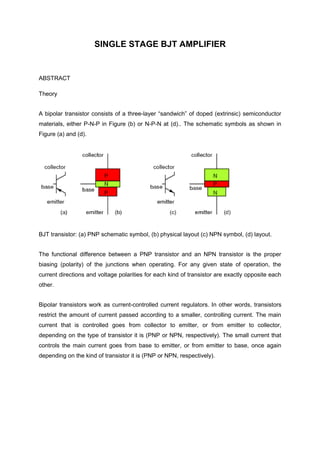
  • 1. SINGLE STAGE BJT AMPLIFIER ABSTRACT Theory A bipolar transistor consists of a three-layer “sandwich” of doped (extrinsic) semiconductor materials, either P-N-P in Figure (b) or N-P-N at (d).. The schematic symbols as shown in Figure (a) and (d). BJT transistor: (a) PNP schematic symbol, (b) physical layout (c) NPN symbol, (d) layout. The functional difference between a PNP transistor and an NPN transistor is the proper biasing (polarity) of the junctions when operating. For any given state of operation, the current directions and voltage polarities for each kind of transistor are exactly opposite each other. Bipolar transistors work as current-controlled current regulators. In other words, transistors restrict the amount of current passed according to a smaller, controlling current. The main current that is controlled goes from collector to emitter, or from emitter to collector, depending on the type of transistor it is (PNP or NPN, respectively). The small current that controls the main current goes from base to emitter, or from emitter to base, once again depending on the kind of transistor it is (PNP or NPN, respectively).
  • 2. The are three types of configurations: 1) Common Emitter Configuration Here the emitter terminal is common to both the input and output signal. The arrangement is the same for a PNP transistor. Used in this way the transistor has the advantages of a medium input impedance, medium output impedance, high voltage gain and high current gain. 2) Common Base Configuration Here the base is the common terminal. Used frequently for RF applications, this stage has the following properties. Low input impedance, high output impedance, unity (or less) current gain and high voltage gain. 3) Common Collector Configuration This last configuration is also more commonly known as the emitter follower. This is because the input signal applied at the base is follow quite closely at the emitter with a voltage gain close to unity. The properties are a high input impedance, a very low output impedance, a unity voltage gain and a high current gain. This circuit is also used extensively as a buffer converting impedances or for feeding or driving long cables or low impedance loads. Characteristic Common Base Common Emitter Common Collector Voltage Gain,Av High Medium Unity Current Gain,Ai Less than unity Medium High Power Gain Low High Medium Input impedance,Zin Low Medium High Output impedance,Zout High Medium Low The main objectives of this experiment are 1) To differentiate the BJT configuration 2) To measure the dc and ac parameters of BJT
  • 3. 3) To observe the differences of voltage gain by common emitter and common collector circuit 4) To observe the waveform differences between the voltage output and voltage input List of equipment was used in this experiment Equiment Component 1) DC Power supply 1) Breadboard 2) Oscilloscope 2) Transistor:BC 109 3) Digital multimeter 3) Resistor:1kΩ,3.3kΩ,27kΩ,120kΩ 4) Function generator 4) Capacitors:10µF,47 µF,22 µF 5) Connecting wires and clippers EXPERIMENT PROCEDURE 1) The Circuit was constructed as shown in Figure 6.2. 2) The Value of VB,VC,VE,VBE and VCE was recorded and measured in Table 6.2.The Amplifier was designed to function with the following bias:VBE~0.7V and VC 0.5Vcc. 3) A 1kHz,20mVp-p signal was applied from signal generator to the amplifier and the input and output signals on the oscilloscope was observed.The input voltage,Vin was slowly increased until the output voltage achieves maximum value without distortion.The input and output waveform was drawed to identify of configuration being used,in Figure 6.4(a) and Figure 6.4(b) respectively. 4) The voltage output,Vo was measured and the voltage gain,Av was calculated by using Equation 6.1 (Equation 6.1) 5) Step 3 and 4 for the circuit shown in Figure 6.3 was repeated,The input and output waveform was drawed in Figure 6.5(a) and Figure 6.5(b) respectively.
  • 4.
  • 5. RESULTS VB VC VE VCE VBE Theoretical 2.755V 9.84V 2.055V 6.16V 0.7V {Pre-Lab) Measured 2.5V 8.6V 1.92V 6.65V 0.64V Table 6.2
  • 6. Discussion In the Figure 6.2 the type of configuration was used is the common emitter configuration and in the Figure 6.3 the type of configuration was used is common collector configuration.From our result it clearly indicate that circuit which is use common emitter configuration amplified the circuit and the circuit which is used common collector configuration does not amplified.So the experiment that was be done agreed with the theory which are voltage gain by the common emitter circuit is high and voltage gain by the common collector circuit is unity. From the result which in table 6.2.It show us that got differences in value between the theoretical and measured.By using theoretical we was using DC Analysis to find out the value VB,VC,VE,VCE by assume B=380 and VBe=0.7.By using digital multimeter we was measured the value VB,VC,VE,VCE,VBE by constructing same circuit in the Figure 6.2 and Figure 6.3.The value slightly differences .So we expect that some error was interrupted our experiment value.One of the error is the instrument error.Each component that we used got some resistance .So it can affect our measured value.
  • 7. References 1) Charles K.Alexander & Mattgew N.O.Sadiku (2009).Fundamentals Of Electrical Circuit Fourth Edition:McGRAW HILL. 2) Norsabrina Sihab (2011), Chapter 4 : DC Analysis of BJT notes