1. STR-X6737
Features and Benefits
▪ Quasi-resonant topology IC Low EMI noise and soft
switching
▪ Bottom-skip mode Improved system efficiency over
the entire output load by avoiding increase of switching
frequency
▪ Auto-Standby mode Lowers input power at very light
output load condition
▪ Avalanche-guaranteed MOSFET Improves system-level
reliability and does not require VDSS derating
▪ 500 VDSS / 0.36 Ω RDS(on)
▪ Various protections Improved system-level reliability
▫ Pulse-by-pulse drain overcurrent limiting
▫ Overvoltage Protection (bias winding voltage sensing),
with latch
▫ Overload Protection with latch
▫ Maximum on-time limit
Off-Line Quasi-Resonant Switching Regulators
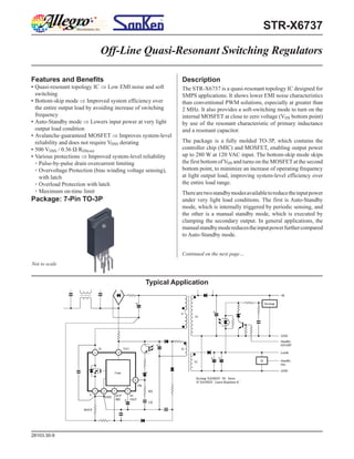
Typical Application
Not to scale
Package: 7-Pin TO-3P
Description
The STR-X6737 is a quasi-resonant topology IC designed for
SMPS applications. It shows lower EMI noise characteristics
than conventional PWM solutions, especially at greater than
2 MHz. It also provides a soft-switching mode to turn on the
internal MOSFET at close to zero voltage (VDS bottom point)
by use of the resonant characteristic of primary inductance
and a resonant capacitor.
The package is a fully molded TO-3P, which contains the
controller chip (MIC) and MOSFET, enabling output power
up to 280 W at 120 VAC input. The bottom-skip mode skips
the first bottom ofVDS and turns on the MOSFETat the second
bottom point, to minimize an increase of operating frequency
at light output load, improving system-level efficiency over
the entire load range.
Therearetwostandbymodesavailabletoreducetheinputpower
under very light load conditions. The first is Auto-Standby
mode, which is internally triggered by periodic sensing, and
the other is a manual standby mode, which is executed by
clamping the secondary output. In general applications, the
manualstandbymodereducestheinputpowerfurthercompared
to Auto-Standby mode.
Continued on the next page…
28103.30-9
2. Off-Line Quasi-Resonant Switching RegulatorsSTR-X6737
2
Thesoft-startmodeminimizessurgevoltageandreducespowerstress
to the MOSFET and to the secondary rectifying diodes during the
start-upsequence.Variousprotectionssuchasovervoltage,overload,
overcurrent, maximum on-time protections and avalanche-energy-
guaranteed MOSFET secure good system-level reliability.
Applications include the following:
▪ Set Top Box
▪ LCD PC monitor, LCD TV
▪ Printer, Scanner
▪ SMPS power supplies
Description (continued)
All performance characteristics given are typical values for circuit or
system baseline design only and are at the nominal operating voltage and
an ambient temperature, TA, of 25°C, unless otherwise stated.
Absolute Maximum Ratings at TA = 25°C
Parameter Symbol Conditions Rating Unit
Drain Current1 IDpeak Single pulse 22 A
Maximum Switching Current2 IDmax TA = –20°C to 125°C 22 A
Single Pulse Avalanche Energy3 EAS Single pulse, VDD = 30 V, L = 50 mH, ILpeak = 3.0 A 239 mJ
Input Voltage for Controller (MIC) VCC 35 V
SS/OLP Terminal Voltage VSSOLP –0.5 to 6.0 V
FB Terminal Inflow Current IFB 10 mA
FB Terminal Voltage VFB IFB within the limits of IFB –0.5 to 9.0 V
OCP/BD Terminal Voltage VOCPBD –1.5 to 5.0 V
MOSFET Power Dissipation4 PD1
With infinite heatsink 44 W
Without heatsink 2.8 W
Controller (MIC) Power Dissipation PD2 VCC × ICC 0.8 W
Operating Internal Leadframe Temperature TF Recommended operation temperature, see cautions –20 to 125 °C
Operating Ambient Temperature TOP –20 to 125 °C
Storage Temperature Tstg –40 to 125 °C
Channel Temperature Tch 150 °C
1Refer to MOSFET ASO curve
2IDMAX is the drain current determined by the drive voltage of the IC and the threshold voltage, Vth, of the MOSFET
3Refer to Avalanche Energy Derating curve
4Refer to MOSFET Ta-PD1 curve
Selection Guide
Part Number Package
STR-X6737 TO-3P
Allegro MicroSystems, Inc.
115 Northeast Cutoff
Worcester, Massachusetts 01615-0036 U.S.A.
1.508.853.5000; www.allegromicro.com
3. Off-Line Quasi-Resonant Switching RegulatorsSTR-X6737
3
Terminal List Table
Number Name Description Functions
1 D Drain MOSFET drain
2 S Source MOSFET source
3 GND Ground terminal Ground
4 VCC Power supply terminal Input of power supply for control circuit
5 SS/OLP Soft Start/Overload Protection terminal Input to set delay for Overload Protection and Soft Start operation
6 FB Feedback terminal
Input for Constant Voltage Control and Burst (intermittent) Mode
oscillation control signals
7 OCP/BD Overcurrent Protection/Bottom Detection Input for Overcurrent Detection and Bottom Detection signals
Functional
Block Diagram
Allegro MicroSystems, Inc.
115 Northeast Cutoff
Worcester, Massachusetts 01615-0036 U.S.A.
1.508.853.5000; www.allegromicro.com
4. Off-Line Quasi-Resonant Switching RegulatorsSTR-X6737
4
0.01
0.1
1
10
100
1 10 100 1000
ID[A]
DrainCurrent
VDS[V]
Drain-to-Source Voltage
STR-X6737
MOSFET A.S.O. Curve
Apply A.S.O temerature
coefficinet from the left graph to
this curve for evaluating actual
operation's safety
Ta=25℃ Single pluse
Determuned by On-Resistance
1ms
100μs
0
20
40
60
80
100
25 50 75 100 125 150
EAStemperaturederatingcoefficient(%)
Tch [℃]
Channeltemperature
STR-X6737
Avalanche energy derating curve
0
20
40
60
80
100
0 20 40 60 80 100 120
A.S.O.temperaturederatingcoefficient(%)
TF [℃]
Internalframetemperature
STR-X6737
A.S.O. temperaturederatingcoefficientCurve
Allegro MicroSystems, Inc.
115 Northeast Cutoff
Worcester, Massachusetts 01615-0036 U.S.A.
1.508.853.5000; www.allegromicro.com
6. Off-Line Quasi-Resonant Switching RegulatorsSTR-X6737
6
ELECTRICAL CHARACTERISTICS
Characteristic Symbol Test Conditions Min. Typ. Max. Units
ELECTRICAL CHARACTERISTICS for Controller (MIC)1, valid at TA = 25°C, VCC = 20 V, unless otherwise specified
Power Supply Start-up Operation
Operation Start Voltage VCC(ON) VCC = 0→20 V 16.3 18.2 19.9 V
Operation Stop Voltage VCC(OFF) VCC = 20→8.8 V 8.8 9.7 10.6 V
Circuit Current In Operation ICC(ON) – – 6 mA
Circuit Current In Non-Operation ICC(OFF) VCC = 15 V – – 100 μA
Oscillation Frequency fosc 19 22 25 kHz
Soft Start Operation Stop Voltage VSSOLP(SS) VSS/OLP increasing 1.1 1.2 1.4 V
Soft Start Operation Charging Current ISSOLP(SS) VSS/OLP = 0 V –710 –550 –390 μA
Normal Operation
Bottom-Skip Operation Threshold Voltage 1 VOCPBD(BS1) –0.720 –0.665 –0.605 V
Bottom-Skip Operation Threshold Voltage 2 VOCPBD(BS2) –0.485 –0.435 –0.385 V
Overcurrent Detection Threshold Voltage VOCPBD(LIM) VOCP/BD falling –0.995 –0.940 –0.895 V
OCP/BD Terminal Outflow Current IOCPBD VOCP/BD = –0.95 V –250 –100 –40 μA
Quasi-Resonant Operation Threshold Voltage 1 VOCPBD(TH1) VOCP/BD falling 0.28 0.40 0.52 V
Quasi-Resonant Operation Threshold Voltage 2 VOCPBD(TH2) VOCP/BD rising 0.67 0.80 0.93 V
FB Terminal Threshold Voltage VFB(OFF) VFB rising 1.32 1.45 1.58 V
FB Terminal Inflow Current (Normal Operation) IFB(ON) VFB = 1.6 V 600 1000 1400 μA
Standby Operation
Standby Operation Start Voltage VCC(S) VCC = 0→15 V, VFB = 1.6 V 10.3 11.2 12.1 V
Standby Operation Start Voltage Interval VCC(SK) VCC(SK) = VCC(S) – VCC(OFF) 1.10 1.35 1.65 V
Standby Non-Operation Circuit Current ICC(S) VCC = 10.2 V, VFB = 1.6 V – 20 56 μA
FB Terminal Inflow Current, Standby Operation IFB(S) VCC = 10.2 V, VFB = 1.6 V – 4 14 μA
FB Terminal Threshold Voltage, Standby Operation VFB(S) VCC = 15 V, VFB rising 0.55 1.10 1.50 V
Minimum On Time tON(MIN) 0.75 1.10 1.50 μs
Protection Operation
Maximum On Time tON(MAX) 27.5 32.5 39.0 μs
Overload Protection Operation Threshold Voltage VSSOLP(OLP) 4.0 4.9 5.8 V
Overload Protection Operation Charging Current ISSOLP(OLP) VSS/OLP = 2.5 V –16 –11 –6 μA
Overvoltage Protection Operation Voltage VCC(OVP) VCC = 0→30 V 25.5 27.7 29.9 V
Latch Circuit Holding Current2 ICC(H) VCC(OFF)– 0.3 V – 45 140 μA
Latch Circuit Release Voltage2 VCC(La.OFF) VCC = 30→6 V, OVP operating 6.0 7.2 8.5 V
ELECTRICAL CHARACTERISTICS for MOSFET, valid at TA = 25°C, unless otherwise specified
Drain-to-Source Breakdown Voltage VDSS IDSS = 300 μA 500 – – V
Drain Leakage Current IDSS VDSSS = 500 V – – 300 μA
On Resistance RDS(on) IDS = 4.0 A – – 0.36 Ω
Switching Time tf – – 500 ns
Thermal Resistance Rθch-F Channel to internal frame – – 1.09 °C/W
1Current polarity with respect to the IC: positive current indicates current sink at the terminal named, negative current indicates source at the
terminal named.
2The latch circuit means a circuit operated OVP and OLP.
Allegro MicroSystems, Inc.
115 Northeast Cutoff
Worcester, Massachusetts 01615-0036 U.S.A.
1.508.853.5000; www.allegromicro.com
7. Off-Line Quasi-Resonant Switching RegulatorsSTR-X6737
7
Packing Specifications
100 pieces per tray
5 trays per inner carton
(Outer packing dependent on quantity)
Dimensions in millimeters
4 inner cartons per outer carton
500 pieces maximum per inner carton
2000 pieces maximum per outer carton
Dimensions in millimeters
2 inner cartons per outer carton
500 pieces maximum per inner carton
1000 pieces maximum per outer carton
Dimensions in millimeters
388
137
364
356
137
206
177
48
333
Allegro MicroSystems, Inc.
115 Northeast Cutoff
Worcester, Massachusetts 01615-0036 U.S.A.
1.508.853.5000; www.allegromicro.com
8. Off-Line Quasi-Resonant Switching RegulatorsSTR-X6737
8
Package Outline Drawing, TO-3P
Leadframe plating Pb-free. Device composition
includes high-temperature solder (Pb >85%),
which is exempted from the RoHS directive.
Ø3.2±0.2
3.45±0.2
3.35±0.1
5.5±0.2
5.5±0.2
Terminal dimension at lead tip Terminal dimension at lead tip
0.55
+0.2
–0.1
5X 0.65
+0.2
–0.1
23±0.3
Branding
Area
XXXXXXXX
XXXXXXXX
2X 2.54±0.1 4X 1.27±0.1
6
15.6 ±0.2
1.89
+0.2
–0.1
1.33
+0.2
–0.1
2X 0.83
+0.2
–0.1
5X 0.75
+0.2
–0.1
2±0.2
Gate Burr
Gate burr: 0.3 mm (max.)
Terminal core material: Cu
Terminal treatment: Ni plating and Pb-free solder dip
Leadform: 1901
Approximate weight: 6 g
Dimensions in millimeters
XXXXXXXX
Drawing for reference only
Branding codes (exact appearance at manufacturer discretion):
1st line, type: STR
2nd line, subtype: X6737
3rd line, lot: YM DD
Where: Y is the last digit of the year of manufacture
M is the month (1 to 9, O, N, D)
DD is the 2-digit date
Enlargement View A
5.5
REF
4.5 ±0.7
7±0.5
3.3
3
12.5±0.5
3.3±0.5
View A
0.7
Front View (Plan View) Side View
0.7 0.7 0.7
1
2
7
6
3
4
5
Allegro MicroSystems, Inc.
115 Northeast Cutoff
Worcester, Massachusetts 01615-0036 U.S.A.
1.508.853.5000; www.allegromicro.com
9. Off-Line Quasi-Resonant Switching RegulatorsSTR-X6737
9
WARNING — These devices are designed to be operated at lethal voltages and energy levels. Circuit
designs that embody these components must conform with applicable safety requirements. Precau-
tions must be taken to prevent accidental contact with power-line potentials.
The use of an isolation transformer is recommended during circuit development and breadboarding.
Because reliability can be affected adversely by improper storage
environments and handling methods, please observe the following
cautions.
Cautions for Storage
• Ensure that storage conditions comply with the standard
temperature (5°C to 35°C) and the standard relative humidity
(around 40 to 75%); avoid storage locations that experience
extreme changes in temperature or humidity.
• Avoid locations where dust or harmful gases are present and
avoid direct sunlight.
• Reinspect for rust on leads and solderability of products that have
been stored for a long time.
Cautions for Testing and Handling
When tests are carried out during inspection testing and other
standard test periods, protect the products from power surges
from the testing device, shorts between adjacent products, and
shorts to the heatsink.
Remarks About Using Silicone Grease with a Heatsink
• When silicone grease is used in mounting this product on a
heatsink, it shall be applied evenly and thinly. If more silicone
grease than required is applied, it may produce stress.
• Coat the back surface of the product and both surfaces of the
insulating plate to improve heat transfer between the product and
the heatsink.
• Volatile-type silicone greases may permeate the product and
produce cracks after long periods of time, resulting in reduced
heat radiation effect, and possibly shortening the lifetime of the
product.
• Our recommended silicone greases for heat radiation purposes,
which will not cause any adverse effect on the product life, are
indicated below:
Type Suppliers
G746 Shin-Etsu Chemical Co., Ltd.
YG6260 Momentive Performance Materials
SC102 Dow Corning Toray Silicone Co., Ltd.
Heatsink Mounting Method
• Torque When Tightening Mounting Screws. Thermal resistance
increases when tightening torque is low, and radiation effects are
decreased. When the torque is too high, the screw can strip, the heatsink
can be deformed, and distortion can arise in the product frame. To avoid
these problems, observe the recommended tightening torques for this
product package type, TO-3P: 0.588 to 0.785 N•m (6 to 8 kgf•cm).
• For effective heat transfer, the contact area between the product and
the heatsink should be free from burrs and metal fragments, and the
heatsink should be flat and large enough to contact over the entire
side of the product, including mounting flange and exposed thermal
pad, and have a minimal mounting hole to prevent possible deflection
and cracking of the product case when fastened to the heatsink.
Soldering
• When soldering the products, please be sure to minimize the
working time, within the following limits:
260±5°C 10 s
350±5°C 3 s
• Soldering iron should be at a distance of at least 1.5 mm from the
body of the products
Electrostatic Discharge
• When handling the products, operator must be grounded.
Grounded wrist straps worn should have at least 1 MΩ of
resistance to ground to prevent shock hazard.
• Workbenches where the products are handled should be
grounded and be provided with conductive table and floor mats.
• When using measuring equipment such as a curve tracer, the
equipment should be grounded.
• When soldering the products, the head of soldering irons or the
solder bath must be grounded in other to prevent leak voltages
generated by them from being applied to the products.
• The products should always be stored and transported in our
shipping containers or conductive containers, or be wrapped in
aluminum foil.
Recommended operation temperature
• Inner frame temperature in operation TF = 115°C
Allegro MicroSystems, Inc.
115 Northeast Cutoff
Worcester, Massachusetts 01615-0036 U.S.A.
1.508.853.5000; www.allegromicro.com
11. Off-Line Quasi-Resonant Switching RegulatorsSTR-X6737
11
Asia-Pacific
China
Sanken Electric Hong Kong Co., Ltd.
Suite 1026, Ocean Centre, Canton Road
Tsimshatsui, Kowloon, Hong Kong
Tel: 852-2735-5262, Fax: 852-2735-5494
Sanken Electric (Shanghai) Co., Ltd.
Room 3202, Maxdo Centre, Xingyi Road 8
Changning District, Shanghai, China
Tel: 86-21-5208-1177, Fax: 86-21-5208-1757
Taiwan Sanken Electric Co., Ltd.
Room 1801, 18th Floor, 88 Jung Shiau East Road
Sec. 2, Taipei 100, Taiwan R.O.C.
Tel: 886-2-2356-8161, Fax: 886-2-2356-8261
Japan
Sanken Electric Co., Ltd.
Overseas Sales Headquarters
Metropolitan Plaza Building, 1-11-1 Nishi-Ikebukuro
Toshima-ku, Tokyo 171-0021, Japan
Tel: 81-3-3986-6164, Fax: 81-3-3986-8637
Korea
Sanken Electric Korea Co., Ltd.
Mirae Asset Life Building, 6F
168 Kongduk-dong, Mapo-ku
Seoul 121-705, Korea
Tel: 82-2-714-3700, Fax: 82-2-3272-2145
Singapore
Sanken Electric Singapore Pte. Ltd.
150 Beach Road, #14-03 The Gateway West
Singapore 189720
Tel: 65-6291-4755, Fax: 65-6297-1744
Europe
Sanken Power Systems (UK) Limited
Pencoed Technology Park
Pencoed, Bridgend CF35 5HY, United Kingdom
Tel: 44-1656-869-100, Fax: 44-1656-869-162
North America
United States
Allegro MicroSystems, Inc.
115 Northeast Cutoff
Worcester, Massachusetts 01606, U.S.A.
Tel: 1-508-853-5000, Fax: 1-508-853-7895
Allegro MicroSystems, Inc.
14 Hughes Street, Suite B105
Irvine, California 92618, U.S.A.
Tel: 1-949-460-2003, Fax: 1-949-460-7837
Worldwide Contacts
Allegro MicroSystems, Inc.
115 Northeast Cutoff
Worcester, Massachusetts 01615-0036 U.S.A.
1.508.853.5000; www.allegromicro.com