SlideShare a Scribd company logo
1 of 7
Download to read offline
Special 80386 Registers
There are three special type of registers in 80386. These are discussed below in
details:

Special
Registers

Control Reg

Debug Reg

Test Reg

CR0-CR3

DR0-DR7

TR6-TR7

Control registers
CR0

The CR0 register is 32 bits long on the 80386 and higher processors. On x86-64 processors in
long mode, it (and the other control registers) is 64 bits long. CR0 has various control flags
that modify the basic operation of the processor.

Bit Name

Full Name

31 PG

Paging

30 CD

Cache disable
Not-write
through

29 NW
18 AM

Alignment mask

16 WP

Write protect

5

NE

Numeric error

4

ET

Extension type

3

TS

Task switched

Description
If 1, enable paging and use the CR3 register, else disable
paging
Globally enables/disable the memory cache
Globally enables/disable write-back caching
Alignment check enabled if AM set, AC flag (in EFLAGS
register) set, and privilege level is 3
Determines whether the CPU can write to pages marked readonly
Enable internal x87 floating point error reporting when set, else
enables PC style x87 error detection
On the 386, it allowed to specify whether the external math
coprocessor was an 80287 or 80387
Allows saving x87 task context upon a task switch only after
2

EM

1

MP

0

PE

Emulation
Monitor coprocessor
Protected Mode
Enable

x87 instruction used
If set, no x87 floating point unit present, if clear, x87 FPU
present
Controls interaction of WAIT/FWAIT instructions with TS flag
in CR0
If 1, system is in protected mode, else system is in real mode

CR1

Reserved
CR2

Contains a value called Page Fault Linear Address (PFLA). When a page fault occurs, the
address the program attempted to access is stored in the CR2 register.
CR3

Typical use of CR3 in address translation with 4 KiB pages.

Used when virtual addressing is enabled, hence when the PG bit is set in CR0. CR3 enables
the processor to translate linear addresses into physical addresses by locating the page
directory and page tables for the current task. Typically, the upper 20 bits of CR3 become the
page directory base register (PDBR), which stores the physical address of the first page
directory entry.
CR4

Used in protected mode to control operations such as virtual-8086 support, enabling I/O
breakpoints, page size extension and machine check exceptions.
Bit

Name

21 SMAP
20 SMEP
18 OSXSAVE
17 PCIDE

Full Name
Supervisor Mode Access
Protection Enable
Supervisor Mode Execution
Protection Enable
XSAVE and Processor
Extended States Enable
PCID Enable

Safer Mode Extensions
Enable
Virtual Machine Extensions
13 VMXE
Enable
Operating System Support for
10 OSXMMEXCPT Unmasked SIMD FloatingPoint Exceptions
Operating system support for
9 OSFXSR
FXSAVE and FXRSTOR
instructions
14 SMXE

8

PCE

Performance-Monitoring
Counter enable

7

PGE

Page Global Enabled

6

MCE

Machine Check Exception

5

PAE

Physical Address Extension

4

PSE

Page Size Extension

3

DE

Debugging Extensions

2

TSD

Time Stamp Disable

1

PVI

Protected-mode Virtual
Interrupts

0

VME

Virtual 8086 Mode
Extensions

Description
If set, access of data in a higher ring
generates a fault[1]
If set, execution of code in a higher ring
generates a fault

If set, enables process-context
identifiers (PCIDs).
see Trusted Execution Technology
(TXT)
see Intel VT-x
If set, enables unmasked SSE
exceptions.
If set, enables SSE instructions and fast
FPU save & restore
If set, RDPMC can be executed at any
privilege level, else RDPMC can only
be used in ring 0.
If set, address translations (PDE or PTE
records) may be shared between address
spaces.
If set, enables machine check interrupts
to occur.
If set, changes page table layout to
translate 32-bit virtual addresses into
extended 36-bit physical addresses.
If unset, page size is 4 KiB, else page
size is increased to 4 MiB (or 2 MiB
with PAE set).
If set, enables debug register based
breaks on I/O space access
If set, RDTSC instruction can only be
executed when in ring 0, otherwise
RDTSC can be used at any privilege
level.
If set, enables support for the virtual
interrupt flag (VIF) in protected mode.
If set, enables support for the virtual
interrupt flag (VIF) in virtual-8086
mode.
Debug Registers
Six 80386 registers are used to control debug features. These registers are accessed by variants of
the MOV instruction. A debug register may be either the source operand or destination operand.
The debug registers are privileged resources; the MOV instructions that access them can only be
executed at privilege level zero. An attempt to read or write the debug registers when executing at
any other privilege level causes a general protection exception. Figure 12-1 shows the format of the
debug registers.

12.2.1 Debug Address Registers (DR0-DR3)
Each of these registers contains the linear address associated with one of four breakpoint
conditions. Each breakpoint condition is further defined by bits in DR7.

The debug address registers are effective whether or not paging is enabled. The addresses in
these registers are linear addresses. If paging is enabled, the linear addresses are translated
into physical addresses by the processor's paging mechanism (as explained in Chapter 5 ) . If
paging is not enabled, these linear addresses are the same as physical addresses.
Note that when paging is enabled, different tasks may have different linear-to-physical
address mappings. When this is the case, an address in a debug address register may be
relevant to one task but not to another. For this reason the 80386 has both global and local
enable bits in DR7. These bits indicate whether a given debug address has a global (all tasks)
or local (current task only) relevance.

12.2.2 Debug Control Register (DR7)
The debug control register shown in Figure 12-1 both helps to define the debug conditions and
selectively enables and disables those conditions.

For each address in registers DR0-DR3, the corresponding fields R/W0 through R/W3
specify the type of action that should cause a breakpoint. The processor interprets these bits
as follows:





00 -- Break on instruction execution only
01 -- Break on data writes only
10 -- undefined
11 -- Break on data reads or writes but not instruction fetches

Fields LEN0 through LEN3 specify the length of data item to be monitored. A length of 1, 2, or 4
bytes may be specified. The values of the length fields are interpreted as follows:





00 -- one-byte length
01 -- two-byte length
10 -- undefined
11 -- four-byte length

If RWn is 00 (instruction execution), then LENn should also be 00. Any other length is undefined.

The low-order eight bits of DR7 (L0 through L3 and G0 through G3) selectively enable the
four address breakpoint conditions. There are two levels of enabling: the local (L0 through
L3) and global (G0 through G3) levels. The local enable bits are automatically reset by the
processor at every task switch to avoid unwanted breakpoint conditions in the new task. The
global enable bits are not reset by a task switch; therefore, they can be used for conditions
that are global to all tasks.
The LE and GE bits control the "exact data breakpoint match" feature of the processor. If
either LE or GE is set, the processor slows execution so that data breakpoints are reported on
the instruction that causes them. It is recommended that one of these bits be set whenever
data breakpoints are armed. The processor clears LE at a task switch but does not clear GE.

12.2.3 Debug Status Register (DR6)
The debug status register shown in Figure 12-1 permits the debugger to determine which debug
conditions have occurred.
When the processor detects an enabled debug exception, it sets the low-order bits of this
register (B0 thru B3) before entering the debug exception handler. Bn is set if the condition
described by DRn, LENn, and R/Wn occurs. (Note that the processor sets Bn regardless of
whether Gn or Ln is set. If more than one breakpoint condition occurs at one time and if the
breakpoint trap occurs due to an enabled condition other than n, Bn may be set, even though
neither Gn nor Ln is set.)
The BT bit is associated with the T-bit (debug trap bit) of the TSS (refer to 7 for the location
of the T-bit). The processor sets the BT bit before entering the debug handler if a task switch
has occurred and the T-bit of the new TSS is set. There is no corresponding bit in DR7 that
enables and disables this trap; the T-bit of the TSS is the sole enabling bit.
The BS bit is associated with the TF (trap flag) bit of the EFLAGS register. The BS bit is set
if the debug handler is entered due to the occurrence of a single-step exception. The singlestep trap is the highest-priority debug exception; therefore, when BS is set, any of the other
debug status bits may also be set.
The BD bit is set if the next instruction will read or write one of the eight debug registers and
ICE-386 is also using the debug registers at the same time.
Note that the bits of DR6 are never cleared by the processor. To avoid any confusion in
identifying the next debug exception, the debug handler should move zeros to DR6
immediately before returning.

Breakpoint Field Recognition
The linear address and LEN field for each of the four breakpoint conditions define a range of
sequential byte addresses for a data breakpoint. The LEN field permits specification of a one, two-, or four-byte field. Two-byte fields must be aligned on word boundaries (addresses that
are multiples of two) and four-byte fields must be aligned on doubleword boundaries
(addresses that are multiples of four). These requirements are enforced by the processor; it
uses the LEN bits to mask the low-order bits of the addresses in the debug address registers.
Improperly aligned code or data breakpoint addresses will not yield the expected results.
A data read or write breakpoint is triggered if any of the bytes participating in a memory
access is within the field defined by a breakpoint address register and the corresponding LEN
field. Table 12-1 gives some examples of breakpoint fields with memory references that both
do and do not cause traps.
To set a data breakpoint for a misaligned field longer than one byte, it may be desirable to put
two sets of entries in the breakpoint register such that each entry is properly aligned and the
two entries together span the length of the field.
Instruction breakpoint addresses must have a length specification of one byte (LEN = 00);
other values are undefined. The processor recognizes an instruction breakpoint address only
when it points to the first byte of an instruction. If the instruction has any prefixes, the
breakpoint address must point to the first prefix.
TEST REGISTER
A test register, in the Intel 80486 processor, was a register used by the processor, usually to
do a self-test. Most of these registers were undocumented, and used by specialized software.
The test registers were named TR3 to TR7. Regular programs don't usually require these
registers to work. With the Pentium, the test registers were replaced by a variety of modelspecific registers (MSRs).
Two test registers, TR6 and TR7, were provided for the purpose of testing. TR6 was the test
command register, and TR7 was the test data register. These registers were accessed by
variants of the MOV instruction. A test register may either be the source operand or the
destination operand. The MOV instructions are defined in both real-address mode and
protected mode. The test registers are privileged resources. In protected mode, the MOV
instructions that access them can only be executed at privilege level 0. An attempt to read or
write the test registers when executing at any other privilege level causes a general protection
exception. Also, those instructions generate invalid opcode exception on any CPU newer than
80486.

More Related Content

What's hot

Architecture of 8086 Microprocessor
Architecture of 8086 Microprocessor  Architecture of 8086 Microprocessor
Architecture of 8086 Microprocessor Mustapha Fatty
 
8237 dma controller
8237 dma controller8237 dma controller
8237 dma controllerTech_MX
 
Interfacing memory with 8086 microprocessor
Interfacing memory with 8086 microprocessorInterfacing memory with 8086 microprocessor
Interfacing memory with 8086 microprocessorVikas Gupta
 
80386 microprocessor system instruction
80386 microprocessor system instruction80386 microprocessor system instruction
80386 microprocessor system instructionUmesh Talware
 
80486 microprocessor
80486 microprocessor80486 microprocessor
80486 microprocessorMihika Shah
 
Instruction set of 8086
Instruction set of 8086Instruction set of 8086
Instruction set of 8086Vijay Kumar
 
Instruction set of 8086
Instruction set of 8086Instruction set of 8086
Instruction set of 80869840596838
 
Logic, shift and rotate instruction
Logic, shift and rotate instructionLogic, shift and rotate instruction
Logic, shift and rotate instructionkashif Shafqat
 
8086 instructions
8086 instructions8086 instructions
8086 instructionsRavi Anand
 
flag register of 8086
flag register of 8086flag register of 8086
flag register of 8086asrithak
 
Asynchronous data transfer
Asynchronous data transferAsynchronous data transfer
Asynchronous data transferpriya Nithya
 
Dynamic debugging in 8085 microprocessor
Dynamic debugging in 8085 microprocessorDynamic debugging in 8085 microprocessor
Dynamic debugging in 8085 microprocessorRamaPrabha24
 
Direct memory access (dma)
Direct memory access (dma)Direct memory access (dma)
Direct memory access (dma)Zubair Khalid
 
Addressing modes of 8086
Addressing modes of 8086Addressing modes of 8086
Addressing modes of 8086saurav kumar
 
Signed Addition And Subtraction
Signed Addition And SubtractionSigned Addition And Subtraction
Signed Addition And SubtractionKeyur Vadodariya
 
Architecture of 80286 microprocessor
Architecture of 80286 microprocessorArchitecture of 80286 microprocessor
Architecture of 80286 microprocessorSyed Ahmed Zaki
 

What's hot (20)

Architecture of 8086 Microprocessor
Architecture of 8086 Microprocessor  Architecture of 8086 Microprocessor
Architecture of 8086 Microprocessor
 
8237 dma controller
8237 dma controller8237 dma controller
8237 dma controller
 
Interfacing memory with 8086 microprocessor
Interfacing memory with 8086 microprocessorInterfacing memory with 8086 microprocessor
Interfacing memory with 8086 microprocessor
 
80386 microprocessor system instruction
80386 microprocessor system instruction80386 microprocessor system instruction
80386 microprocessor system instruction
 
80486 microprocessor
80486 microprocessor80486 microprocessor
80486 microprocessor
 
Instruction set of 8086
Instruction set of 8086Instruction set of 8086
Instruction set of 8086
 
Interrupts of 8086
Interrupts of 8086Interrupts of 8086
Interrupts of 8086
 
Memory System
Memory SystemMemory System
Memory System
 
Instruction set of 8086
Instruction set of 8086Instruction set of 8086
Instruction set of 8086
 
Logic, shift and rotate instruction
Logic, shift and rotate instructionLogic, shift and rotate instruction
Logic, shift and rotate instruction
 
8086 instructions
8086 instructions8086 instructions
8086 instructions
 
flag register of 8086
flag register of 8086flag register of 8086
flag register of 8086
 
Asynchronous data transfer
Asynchronous data transferAsynchronous data transfer
Asynchronous data transfer
 
Dynamic debugging in 8085 microprocessor
Dynamic debugging in 8085 microprocessorDynamic debugging in 8085 microprocessor
Dynamic debugging in 8085 microprocessor
 
Direct memory access (dma)
Direct memory access (dma)Direct memory access (dma)
Direct memory access (dma)
 
Introduction to 80386
Introduction to 80386Introduction to 80386
Introduction to 80386
 
Addressing modes of 8086
Addressing modes of 8086Addressing modes of 8086
Addressing modes of 8086
 
80386 Architecture
80386 Architecture80386 Architecture
80386 Architecture
 
Signed Addition And Subtraction
Signed Addition And SubtractionSigned Addition And Subtraction
Signed Addition And Subtraction
 
Architecture of 80286 microprocessor
Architecture of 80286 microprocessorArchitecture of 80286 microprocessor
Architecture of 80286 microprocessor
 

Similar to Special of 80386 registers

Intel® 80386 microprocessor registers
Intel® 80386 microprocessor registersIntel® 80386 microprocessor registers
Intel® 80386 microprocessor registersNeel Shah
 
Unit 2 se pai_registers in 80386
Unit 2 se pai_registers in 80386Unit 2 se pai_registers in 80386
Unit 2 se pai_registers in 80386KanchanPatil34
 
Memory Access Instructions
Memory Access InstructionsMemory Access Instructions
Memory Access InstructionsSharif Ullah
 
Microprocessor Protected Mode Memory addressing By DHEERAJ KATARIA
Microprocessor Protected Mode Memory addressing By DHEERAJ KATARIAMicroprocessor Protected Mode Memory addressing By DHEERAJ KATARIA
Microprocessor Protected Mode Memory addressing By DHEERAJ KATARIADheeraj Kataria
 
Assembly programming
Assembly programmingAssembly programming
Assembly programmingOmar Sanchez
 
Pentium Multitasking.ppt
Pentium Multitasking.pptPentium Multitasking.ppt
Pentium Multitasking.pptPramodBorole2
 
Arm teaching material
Arm teaching materialArm teaching material
Arm teaching materialJohn Williams
 
arm-instructionset.pdf
arm-instructionset.pdfarm-instructionset.pdf
arm-instructionset.pdfRoopaPatil24
 
arm-instructionset.pdf
arm-instructionset.pdfarm-instructionset.pdf
arm-instructionset.pdfRoopaPatil24
 
Intel x86 Architecture
Intel x86 ArchitectureIntel x86 Architecture
Intel x86 ArchitectureChangWoo Min
 
microprocessor_part_3_compressed_1588259301.pdf
microprocessor_part_3_compressed_1588259301.pdfmicroprocessor_part_3_compressed_1588259301.pdf
microprocessor_part_3_compressed_1588259301.pdfssuserd21262
 
PAI Unit 3 Multitasking in 80386
PAI Unit 3 Multitasking in 80386PAI Unit 3 Multitasking in 80386
PAI Unit 3 Multitasking in 80386KanchanPatil34
 

Similar to Special of 80386 registers (20)

Intel® 80386 microprocessor registers
Intel® 80386 microprocessor registersIntel® 80386 microprocessor registers
Intel® 80386 microprocessor registers
 
x86_1.ppt
x86_1.pptx86_1.ppt
x86_1.ppt
 
Protection mode
Protection modeProtection mode
Protection mode
 
Unit 2 se pai_registers in 80386
Unit 2 se pai_registers in 80386Unit 2 se pai_registers in 80386
Unit 2 se pai_registers in 80386
 
Memory Access Instructions
Memory Access InstructionsMemory Access Instructions
Memory Access Instructions
 
Microprocessor Protected Mode Memory addressing By DHEERAJ KATARIA
Microprocessor Protected Mode Memory addressing By DHEERAJ KATARIAMicroprocessor Protected Mode Memory addressing By DHEERAJ KATARIA
Microprocessor Protected Mode Memory addressing By DHEERAJ KATARIA
 
Internal microprocessor architecture
Internal microprocessor architectureInternal microprocessor architecture
Internal microprocessor architecture
 
486 or 80486 DX Architecture
486 or 80486 DX Architecture486 or 80486 DX Architecture
486 or 80486 DX Architecture
 
Assembly programming
Assembly programmingAssembly programming
Assembly programming
 
Pentium Multitasking.ppt
Pentium Multitasking.pptPentium Multitasking.ppt
Pentium Multitasking.ppt
 
Arm teaching material
Arm teaching materialArm teaching material
Arm teaching material
 
Arm teaching material
Arm teaching materialArm teaching material
Arm teaching material
 
Arm11
Arm11Arm11
Arm11
 
Memory mgmt 80386
Memory mgmt 80386Memory mgmt 80386
Memory mgmt 80386
 
arm-instructionset.pdf
arm-instructionset.pdfarm-instructionset.pdf
arm-instructionset.pdf
 
arm-instructionset.pdf
arm-instructionset.pdfarm-instructionset.pdf
arm-instructionset.pdf
 
Intel x86 Architecture
Intel x86 ArchitectureIntel x86 Architecture
Intel x86 Architecture
 
Lecture9
Lecture9Lecture9
Lecture9
 
microprocessor_part_3_compressed_1588259301.pdf
microprocessor_part_3_compressed_1588259301.pdfmicroprocessor_part_3_compressed_1588259301.pdf
microprocessor_part_3_compressed_1588259301.pdf
 
PAI Unit 3 Multitasking in 80386
PAI Unit 3 Multitasking in 80386PAI Unit 3 Multitasking in 80386
PAI Unit 3 Multitasking in 80386
 

Recently uploaded

APM Welcome, APM North West Network Conference, Synergies Across Sectors
APM Welcome, APM North West Network Conference, Synergies Across SectorsAPM Welcome, APM North West Network Conference, Synergies Across Sectors
APM Welcome, APM North West Network Conference, Synergies Across SectorsAssociation for Project Management
 
This PowerPoint helps students to consider the concept of infinity.
This PowerPoint helps students to consider the concept of infinity.This PowerPoint helps students to consider the concept of infinity.
This PowerPoint helps students to consider the concept of infinity.christianmathematics
 
Gardella_PRCampaignConclusion Pitch Letter
Gardella_PRCampaignConclusion Pitch LetterGardella_PRCampaignConclusion Pitch Letter
Gardella_PRCampaignConclusion Pitch LetterMateoGardella
 
Web & Social Media Analytics Previous Year Question Paper.pdf
Web & Social Media Analytics Previous Year Question Paper.pdfWeb & Social Media Analytics Previous Year Question Paper.pdf
Web & Social Media Analytics Previous Year Question Paper.pdfJayanti Pande
 
psychiatric nursing HISTORY COLLECTION .docx
psychiatric  nursing HISTORY  COLLECTION  .docxpsychiatric  nursing HISTORY  COLLECTION  .docx
psychiatric nursing HISTORY COLLECTION .docxPoojaSen20
 
Making and Justifying Mathematical Decisions.pdf
Making and Justifying Mathematical Decisions.pdfMaking and Justifying Mathematical Decisions.pdf
Making and Justifying Mathematical Decisions.pdfChris Hunter
 
Beyond the EU: DORA and NIS 2 Directive's Global Impact
Beyond the EU: DORA and NIS 2 Directive's Global ImpactBeyond the EU: DORA and NIS 2 Directive's Global Impact
Beyond the EU: DORA and NIS 2 Directive's Global ImpactPECB
 
Advanced Views - Calendar View in Odoo 17
Advanced Views - Calendar View in Odoo 17Advanced Views - Calendar View in Odoo 17
Advanced Views - Calendar View in Odoo 17Celine George
 
Paris 2024 Olympic Geographies - an activity
Paris 2024 Olympic Geographies - an activityParis 2024 Olympic Geographies - an activity
Paris 2024 Olympic Geographies - an activityGeoBlogs
 
The basics of sentences session 2pptx copy.pptx
The basics of sentences session 2pptx copy.pptxThe basics of sentences session 2pptx copy.pptx
The basics of sentences session 2pptx copy.pptxheathfieldcps1
 
Unit-IV- Pharma. Marketing Channels.pptx
Unit-IV- Pharma. Marketing Channels.pptxUnit-IV- Pharma. Marketing Channels.pptx
Unit-IV- Pharma. Marketing Channels.pptxVishalSingh1417
 
Basic Civil Engineering first year Notes- Chapter 4 Building.pptx
Basic Civil Engineering first year Notes- Chapter 4 Building.pptxBasic Civil Engineering first year Notes- Chapter 4 Building.pptx
Basic Civil Engineering first year Notes- Chapter 4 Building.pptxDenish Jangid
 
Holdier Curriculum Vitae (April 2024).pdf
Holdier Curriculum Vitae (April 2024).pdfHoldier Curriculum Vitae (April 2024).pdf
Holdier Curriculum Vitae (April 2024).pdfagholdier
 
Key note speaker Neum_Admir Softic_ENG.pdf
Key note speaker Neum_Admir Softic_ENG.pdfKey note speaker Neum_Admir Softic_ENG.pdf
Key note speaker Neum_Admir Softic_ENG.pdfAdmir Softic
 
fourth grading exam for kindergarten in writing
fourth grading exam for kindergarten in writingfourth grading exam for kindergarten in writing
fourth grading exam for kindergarten in writingTeacherCyreneCayanan
 
Grant Readiness 101 TechSoup and Remy Consulting
Grant Readiness 101 TechSoup and Remy ConsultingGrant Readiness 101 TechSoup and Remy Consulting
Grant Readiness 101 TechSoup and Remy ConsultingTechSoup
 
Z Score,T Score, Percential Rank and Box Plot Graph
Z Score,T Score, Percential Rank and Box Plot GraphZ Score,T Score, Percential Rank and Box Plot Graph
Z Score,T Score, Percential Rank and Box Plot GraphThiyagu K
 

Recently uploaded (20)

APM Welcome, APM North West Network Conference, Synergies Across Sectors
APM Welcome, APM North West Network Conference, Synergies Across SectorsAPM Welcome, APM North West Network Conference, Synergies Across Sectors
APM Welcome, APM North West Network Conference, Synergies Across Sectors
 
Mehran University Newsletter Vol-X, Issue-I, 2024
Mehran University Newsletter Vol-X, Issue-I, 2024Mehran University Newsletter Vol-X, Issue-I, 2024
Mehran University Newsletter Vol-X, Issue-I, 2024
 
This PowerPoint helps students to consider the concept of infinity.
This PowerPoint helps students to consider the concept of infinity.This PowerPoint helps students to consider the concept of infinity.
This PowerPoint helps students to consider the concept of infinity.
 
Gardella_PRCampaignConclusion Pitch Letter
Gardella_PRCampaignConclusion Pitch LetterGardella_PRCampaignConclusion Pitch Letter
Gardella_PRCampaignConclusion Pitch Letter
 
Mattingly "AI & Prompt Design: Structured Data, Assistants, & RAG"
Mattingly "AI & Prompt Design: Structured Data, Assistants, & RAG"Mattingly "AI & Prompt Design: Structured Data, Assistants, & RAG"
Mattingly "AI & Prompt Design: Structured Data, Assistants, & RAG"
 
Web & Social Media Analytics Previous Year Question Paper.pdf
Web & Social Media Analytics Previous Year Question Paper.pdfWeb & Social Media Analytics Previous Year Question Paper.pdf
Web & Social Media Analytics Previous Year Question Paper.pdf
 
psychiatric nursing HISTORY COLLECTION .docx
psychiatric  nursing HISTORY  COLLECTION  .docxpsychiatric  nursing HISTORY  COLLECTION  .docx
psychiatric nursing HISTORY COLLECTION .docx
 
Making and Justifying Mathematical Decisions.pdf
Making and Justifying Mathematical Decisions.pdfMaking and Justifying Mathematical Decisions.pdf
Making and Justifying Mathematical Decisions.pdf
 
Beyond the EU: DORA and NIS 2 Directive's Global Impact
Beyond the EU: DORA and NIS 2 Directive's Global ImpactBeyond the EU: DORA and NIS 2 Directive's Global Impact
Beyond the EU: DORA and NIS 2 Directive's Global Impact
 
Advanced Views - Calendar View in Odoo 17
Advanced Views - Calendar View in Odoo 17Advanced Views - Calendar View in Odoo 17
Advanced Views - Calendar View in Odoo 17
 
Paris 2024 Olympic Geographies - an activity
Paris 2024 Olympic Geographies - an activityParis 2024 Olympic Geographies - an activity
Paris 2024 Olympic Geographies - an activity
 
INDIA QUIZ 2024 RLAC DELHI UNIVERSITY.pptx
INDIA QUIZ 2024 RLAC DELHI UNIVERSITY.pptxINDIA QUIZ 2024 RLAC DELHI UNIVERSITY.pptx
INDIA QUIZ 2024 RLAC DELHI UNIVERSITY.pptx
 
The basics of sentences session 2pptx copy.pptx
The basics of sentences session 2pptx copy.pptxThe basics of sentences session 2pptx copy.pptx
The basics of sentences session 2pptx copy.pptx
 
Unit-IV- Pharma. Marketing Channels.pptx
Unit-IV- Pharma. Marketing Channels.pptxUnit-IV- Pharma. Marketing Channels.pptx
Unit-IV- Pharma. Marketing Channels.pptx
 
Basic Civil Engineering first year Notes- Chapter 4 Building.pptx
Basic Civil Engineering first year Notes- Chapter 4 Building.pptxBasic Civil Engineering first year Notes- Chapter 4 Building.pptx
Basic Civil Engineering first year Notes- Chapter 4 Building.pptx
 
Holdier Curriculum Vitae (April 2024).pdf
Holdier Curriculum Vitae (April 2024).pdfHoldier Curriculum Vitae (April 2024).pdf
Holdier Curriculum Vitae (April 2024).pdf
 
Key note speaker Neum_Admir Softic_ENG.pdf
Key note speaker Neum_Admir Softic_ENG.pdfKey note speaker Neum_Admir Softic_ENG.pdf
Key note speaker Neum_Admir Softic_ENG.pdf
 
fourth grading exam for kindergarten in writing
fourth grading exam for kindergarten in writingfourth grading exam for kindergarten in writing
fourth grading exam for kindergarten in writing
 
Grant Readiness 101 TechSoup and Remy Consulting
Grant Readiness 101 TechSoup and Remy ConsultingGrant Readiness 101 TechSoup and Remy Consulting
Grant Readiness 101 TechSoup and Remy Consulting
 
Z Score,T Score, Percential Rank and Box Plot Graph
Z Score,T Score, Percential Rank and Box Plot GraphZ Score,T Score, Percential Rank and Box Plot Graph
Z Score,T Score, Percential Rank and Box Plot Graph
 

Special of 80386 registers

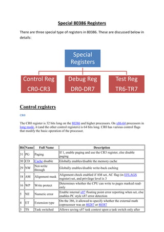
  • 1. Special 80386 Registers There are three special type of registers in 80386. These are discussed below in details: Special Registers Control Reg Debug Reg Test Reg CR0-CR3 DR0-DR7 TR6-TR7 Control registers CR0 The CR0 register is 32 bits long on the 80386 and higher processors. On x86-64 processors in long mode, it (and the other control registers) is 64 bits long. CR0 has various control flags that modify the basic operation of the processor. Bit Name Full Name 31 PG Paging 30 CD Cache disable Not-write through 29 NW 18 AM Alignment mask 16 WP Write protect 5 NE Numeric error 4 ET Extension type 3 TS Task switched Description If 1, enable paging and use the CR3 register, else disable paging Globally enables/disable the memory cache Globally enables/disable write-back caching Alignment check enabled if AM set, AC flag (in EFLAGS register) set, and privilege level is 3 Determines whether the CPU can write to pages marked readonly Enable internal x87 floating point error reporting when set, else enables PC style x87 error detection On the 386, it allowed to specify whether the external math coprocessor was an 80287 or 80387 Allows saving x87 task context upon a task switch only after
  • 2. 2 EM 1 MP 0 PE Emulation Monitor coprocessor Protected Mode Enable x87 instruction used If set, no x87 floating point unit present, if clear, x87 FPU present Controls interaction of WAIT/FWAIT instructions with TS flag in CR0 If 1, system is in protected mode, else system is in real mode CR1 Reserved CR2 Contains a value called Page Fault Linear Address (PFLA). When a page fault occurs, the address the program attempted to access is stored in the CR2 register. CR3 Typical use of CR3 in address translation with 4 KiB pages. Used when virtual addressing is enabled, hence when the PG bit is set in CR0. CR3 enables the processor to translate linear addresses into physical addresses by locating the page directory and page tables for the current task. Typically, the upper 20 bits of CR3 become the page directory base register (PDBR), which stores the physical address of the first page directory entry. CR4 Used in protected mode to control operations such as virtual-8086 support, enabling I/O breakpoints, page size extension and machine check exceptions.
  • 3. Bit Name 21 SMAP 20 SMEP 18 OSXSAVE 17 PCIDE Full Name Supervisor Mode Access Protection Enable Supervisor Mode Execution Protection Enable XSAVE and Processor Extended States Enable PCID Enable Safer Mode Extensions Enable Virtual Machine Extensions 13 VMXE Enable Operating System Support for 10 OSXMMEXCPT Unmasked SIMD FloatingPoint Exceptions Operating system support for 9 OSFXSR FXSAVE and FXRSTOR instructions 14 SMXE 8 PCE Performance-Monitoring Counter enable 7 PGE Page Global Enabled 6 MCE Machine Check Exception 5 PAE Physical Address Extension 4 PSE Page Size Extension 3 DE Debugging Extensions 2 TSD Time Stamp Disable 1 PVI Protected-mode Virtual Interrupts 0 VME Virtual 8086 Mode Extensions Description If set, access of data in a higher ring generates a fault[1] If set, execution of code in a higher ring generates a fault If set, enables process-context identifiers (PCIDs). see Trusted Execution Technology (TXT) see Intel VT-x If set, enables unmasked SSE exceptions. If set, enables SSE instructions and fast FPU save & restore If set, RDPMC can be executed at any privilege level, else RDPMC can only be used in ring 0. If set, address translations (PDE or PTE records) may be shared between address spaces. If set, enables machine check interrupts to occur. If set, changes page table layout to translate 32-bit virtual addresses into extended 36-bit physical addresses. If unset, page size is 4 KiB, else page size is increased to 4 MiB (or 2 MiB with PAE set). If set, enables debug register based breaks on I/O space access If set, RDTSC instruction can only be executed when in ring 0, otherwise RDTSC can be used at any privilege level. If set, enables support for the virtual interrupt flag (VIF) in protected mode. If set, enables support for the virtual interrupt flag (VIF) in virtual-8086 mode.
  • 4. Debug Registers Six 80386 registers are used to control debug features. These registers are accessed by variants of the MOV instruction. A debug register may be either the source operand or destination operand. The debug registers are privileged resources; the MOV instructions that access them can only be executed at privilege level zero. An attempt to read or write the debug registers when executing at any other privilege level causes a general protection exception. Figure 12-1 shows the format of the debug registers. 12.2.1 Debug Address Registers (DR0-DR3) Each of these registers contains the linear address associated with one of four breakpoint conditions. Each breakpoint condition is further defined by bits in DR7. The debug address registers are effective whether or not paging is enabled. The addresses in these registers are linear addresses. If paging is enabled, the linear addresses are translated into physical addresses by the processor's paging mechanism (as explained in Chapter 5 ) . If paging is not enabled, these linear addresses are the same as physical addresses.
  • 5. Note that when paging is enabled, different tasks may have different linear-to-physical address mappings. When this is the case, an address in a debug address register may be relevant to one task but not to another. For this reason the 80386 has both global and local enable bits in DR7. These bits indicate whether a given debug address has a global (all tasks) or local (current task only) relevance. 12.2.2 Debug Control Register (DR7) The debug control register shown in Figure 12-1 both helps to define the debug conditions and selectively enables and disables those conditions. For each address in registers DR0-DR3, the corresponding fields R/W0 through R/W3 specify the type of action that should cause a breakpoint. The processor interprets these bits as follows:     00 -- Break on instruction execution only 01 -- Break on data writes only 10 -- undefined 11 -- Break on data reads or writes but not instruction fetches Fields LEN0 through LEN3 specify the length of data item to be monitored. A length of 1, 2, or 4 bytes may be specified. The values of the length fields are interpreted as follows:     00 -- one-byte length 01 -- two-byte length 10 -- undefined 11 -- four-byte length If RWn is 00 (instruction execution), then LENn should also be 00. Any other length is undefined. The low-order eight bits of DR7 (L0 through L3 and G0 through G3) selectively enable the four address breakpoint conditions. There are two levels of enabling: the local (L0 through L3) and global (G0 through G3) levels. The local enable bits are automatically reset by the processor at every task switch to avoid unwanted breakpoint conditions in the new task. The global enable bits are not reset by a task switch; therefore, they can be used for conditions that are global to all tasks. The LE and GE bits control the "exact data breakpoint match" feature of the processor. If either LE or GE is set, the processor slows execution so that data breakpoints are reported on the instruction that causes them. It is recommended that one of these bits be set whenever data breakpoints are armed. The processor clears LE at a task switch but does not clear GE. 12.2.3 Debug Status Register (DR6) The debug status register shown in Figure 12-1 permits the debugger to determine which debug conditions have occurred.
  • 6. When the processor detects an enabled debug exception, it sets the low-order bits of this register (B0 thru B3) before entering the debug exception handler. Bn is set if the condition described by DRn, LENn, and R/Wn occurs. (Note that the processor sets Bn regardless of whether Gn or Ln is set. If more than one breakpoint condition occurs at one time and if the breakpoint trap occurs due to an enabled condition other than n, Bn may be set, even though neither Gn nor Ln is set.) The BT bit is associated with the T-bit (debug trap bit) of the TSS (refer to 7 for the location of the T-bit). The processor sets the BT bit before entering the debug handler if a task switch has occurred and the T-bit of the new TSS is set. There is no corresponding bit in DR7 that enables and disables this trap; the T-bit of the TSS is the sole enabling bit. The BS bit is associated with the TF (trap flag) bit of the EFLAGS register. The BS bit is set if the debug handler is entered due to the occurrence of a single-step exception. The singlestep trap is the highest-priority debug exception; therefore, when BS is set, any of the other debug status bits may also be set. The BD bit is set if the next instruction will read or write one of the eight debug registers and ICE-386 is also using the debug registers at the same time. Note that the bits of DR6 are never cleared by the processor. To avoid any confusion in identifying the next debug exception, the debug handler should move zeros to DR6 immediately before returning. Breakpoint Field Recognition The linear address and LEN field for each of the four breakpoint conditions define a range of sequential byte addresses for a data breakpoint. The LEN field permits specification of a one, two-, or four-byte field. Two-byte fields must be aligned on word boundaries (addresses that are multiples of two) and four-byte fields must be aligned on doubleword boundaries (addresses that are multiples of four). These requirements are enforced by the processor; it uses the LEN bits to mask the low-order bits of the addresses in the debug address registers. Improperly aligned code or data breakpoint addresses will not yield the expected results. A data read or write breakpoint is triggered if any of the bytes participating in a memory access is within the field defined by a breakpoint address register and the corresponding LEN field. Table 12-1 gives some examples of breakpoint fields with memory references that both do and do not cause traps. To set a data breakpoint for a misaligned field longer than one byte, it may be desirable to put two sets of entries in the breakpoint register such that each entry is properly aligned and the two entries together span the length of the field. Instruction breakpoint addresses must have a length specification of one byte (LEN = 00); other values are undefined. The processor recognizes an instruction breakpoint address only when it points to the first byte of an instruction. If the instruction has any prefixes, the breakpoint address must point to the first prefix.
  • 7. TEST REGISTER A test register, in the Intel 80486 processor, was a register used by the processor, usually to do a self-test. Most of these registers were undocumented, and used by specialized software. The test registers were named TR3 to TR7. Regular programs don't usually require these registers to work. With the Pentium, the test registers were replaced by a variety of modelspecific registers (MSRs). Two test registers, TR6 and TR7, were provided for the purpose of testing. TR6 was the test command register, and TR7 was the test data register. These registers were accessed by variants of the MOV instruction. A test register may either be the source operand or the destination operand. The MOV instructions are defined in both real-address mode and protected mode. The test registers are privileged resources. In protected mode, the MOV instructions that access them can only be executed at privilege level 0. An attempt to read or write the test registers when executing at any other privilege level causes a general protection exception. Also, those instructions generate invalid opcode exception on any CPU newer than 80486.