SlideShare une entreprise Scribd logo
1  sur  8
Télécharger pour lire hors ligne
19-2905; Rev 0; 8/03


                    KIT
              ATION
         EVALU   BLE
           AVAILA


                                                                                         x


                                                                                                                                                                MAX3841
        _______________________________                                                              _______________________________
                                                                                         ◆
                                                                                         ◆
                                                                                         ◆
                                                                                         ◆
                                                                                         ◆
                                                                                         ◆
                                                                                         ◆
                                                                                         ◆
                                                                                         ◆


                                                                                                     _______________________________
                                                                                                                                       PIN-          PKG.
                                                                                                 PART              TEMP RANGE
                                                                                                                                       PACKAGE       CODE
                            _____________________
                                                                                          MAX3841ETG               -40°C to +85°C      24 Thin QFN   T2444-1


                       _______________________________________________________________

                                                                                                                              1.8V

                                                                      2.5V      3.3V         1.8V                           10Gbps
                         3.3V     2.5V                                                                                    CDR/SERDES
                                                                     VCC1OUT     VCC       VCC2IN                            ASIC
                                         SDI+                 OUT1+                                  IN2+              SDO+
                        10Gbps
                         SERIAL          SDI-                 OUT1-                                  IN2-              SDO-
                        OPTICAL                                                MAX3841
                        MODULE       SDO+                     IN1+                                  OUT2+              SDI+

                                     SDO-                     IN1-                                  OUT2-              SDI-
                                                       2.5V                                                 1.8V

                                                              VCC1IN                            VCC2OUT

                                                                 SEL1 SEL2      ENO1     ENO2       GND


                                            LOOPBACK


                       ________________________________________________________________ Maxim Integrated Products                                           1
x
          ABSOLUTE MAXIMUM RATINGS
MAX3841


          Supply Voltage, VCC..............................................-0.5V to +4.0V      Continuous Power Dissipation (TA = +85°C)
          CML Supply Voltage (VCC_IN, VCC_OUT)...........-0.5V to +4.0V                          24-Pin Thin QFN (derate 20.8mW/°C
          Continuous Output Current (OUT1±, OUT2±)...................±25mA                       above +85°C).............................................................1352mW
          CML Input Voltage (IN1±, IN2±)...........-0.5V to (VCC_IN + 0.5V)                    Operating Temperature Range ...........................-40°C to +85°C
          LVCMOS Input Voltage (SEL1, SEL2,                                                    Storage Temperature Range .............................-55°C to +150°C
            ENO1, ENO2) .........................................-0.5V to (VCC + 0.5V)         Lead Temperature (soldering, 10s) .................................+300°C

          Stresses beyond those listed under “Absolute Maximum Ratings” may cause permanent damage to the device. These are stress ratings only, and functional
          operation of the device at these or any other conditions beyond those indicated in the operational sections of the specifications is not implied. Exposure to
          absolute maximum rating conditions for extended periods may affect device reliability.


          ELECTRICAL CHARACTERISTICS
          (VCC = +3.0V to +3.6V, VCC_IN = +1.71V to VCC, VCC_OUT = +1.71V to VCC, TA = -40°C to +85°C. Typical values are at VCC =
          +3.3V, VCC_IN = VCC_OUT = 1.8V, TA = +25°C, unless otherwise noted.)

                       PARAMETER                         SYMBOL                             CONDITIONS                             MIN         TYP         MAX         UNITS
           Core Supply Current                              ICC         Excluding CML termination currents                                      65           90          mA
           Data Rate                                                    (Note 1)                                                    0                       12.5       Gbps
           CML Input Differential                           VIN         AC-coupled or DC-coupled (Note 2)                          150                     1200        mVP-P
           CML Input Common Mode                                        DC-coupled                                              VCC_IN - 0.3             VCC_IN           V
           CML Input Termination                                        Single ended                                              42.5          50          57.5          Ω
           CML Input Return Loss                                        Up to 10GHz                                                             12                       dB
           CML Output Differential                         VOUT         (Note 2)                                                   400         500          600        mVP-P
           CML Output Termination                                       Single ended                                              42.5          50          57.5          Ω
           CML Output Transition Time                      tR, tF       20% to 80% (Notes 1, 3)                                                              30          ps
           Deterministic Jitter                                         (Notes 1, 4)                                                                         10        psP-P
           Random Jitter                                                VIN = 150mVP-P (Notes 1, 5)                                            0.3          0.7        psRMS
           Propagation Delay                                            Any input to output (Note 1)                                           100          140          ps
           Channel-to-Channel Skew                                      (Note 1)                                                                             12          ps
           Output Duty-Cycle Skew                                       50% input duty cycle (Notes 1, 3)                                                     8          ps
           LVCMOS Input Current                            IIH, IIL                                                                -10                      +10          µA
           LVCMOS Input High Voltage                        VIH                                                                    1.7                                    V
          Note 1: Guaranteed by design and characterization.
          Note 2: Differential swing is defined as VIN = (IN_+) - (IN_-) and VOUT = (OUT_+) - (OUT_-). See Figure 1.
          Note 3: Measured using a 0000011111 pattern at 12.5Gbps, and VIN = 400mVP-P differential.
          Note 4: Measured at 9.953Gbps using a pattern of 100 ones, 27 - 1 PRBS, 100 zeros, 27 - 1 PRBS, and at 12.5Gbps using a ±K28.5
                  pattern. VCC_IN = VCC_OUT = 1.8V, and VIN = 400mVP-P differential.
          Note 5: Refer to Maxim application note HFAN-04.5.1: Measuring Random Jitter on a Digital Sampling Oscilloscope.


          2    _______________________________________________________________________________________
x


                                                                                                                                                                                                                                                                          MAX3841
                                                       _______________________________________________________________
(VCC = 3.3V, VCC_IN, VCC_OUT = 1.8V, VIN = 500mVP-P, TA = +25°C, unless otherwise noted.)


                               CORE SUPPLY CURRENT vs. TEMPERATURE                                                                                SUPPLY CURRENT vs. TEMPERATURE                                                OUTPUT EYE DIAGRAM
                                    (EXCLUDES CML I/O CURRENTS)                                                                                     (CORE PLUS CML I/O CURRENTS)                                               (12.5Gbps, 223 - 1 PRBS)
                                                                                                                                                                                                                                                      MAX3841 toc03
                             140                                                                                                          140


                                                                                                                                                                                                    MAX3841 toc02
                                                                                         MAX3841 toc01
                             130                                                                                                          130
                             120                                                                                                          120                   2 OUTPUTS ENABLE


                                                                                                            SUPPLY CURRENT (mA)
SUPPLY CURRENT (mA)


                             110                  0 OUTPUTS ENABLE                                                                        110           1 OUTPUT ENABLE
                             100         1 OUTPUT ENABLE                                                                                  100
                             90                                                                                                           90           0 OUTPUTS ENABLE                                             60mV/div
                             80          2 OUTPUTS ENABLE                                                                                 80
                             70                                                                                                           70
                             60                                                                                                           60
                             50                                                                                                           50
                                                                                                                                                      CML INPUTS AND OUTPUTS AC-COUPLED
                              40                                                                                                           40
                                   -40      -15       10         35     60          85                                                          -40       -15       10       35     60         85                                       14ps/div
                                                   TEMPERATURE (°C)                                                                                              TEMPERATURE (°C)


                                              OUTPUT EYE DIAGRAM                                                                                           OUTPUT EYE DIAGRAM                                                   OUTPUT EYE DIAGRAM
                                             (10.7Gbps, 223 - 1 PRBS)                                                                                     (6.25Gbps, 223 - 1 PRBS)                                             (622Mbps, 223 - 1 PRBS)
                                                                         MAX3841 toc04                                                                                              MAX3841 toc05                                                     MAX3841 toc06


60mV/div                                                                                                   60mV/div                                                                                                 60mV/div


                                                        16ps/div                                                                                                      28ps/div                                                         270ps/div


                                              DETERMINISTIC JITTER                                                                                      DIFFERENTIAL OUTPUT SWING
                                                vs. TEMPERATURE                                                                                              vs. TEMPERATURE                                                    PROPAGATION DELAY
                                                                                                                                                                                                                                                     MAX3841 toc09
                              16                                                                                                          550
                                                                                                                                                                                                    MAX3841 toc08
                                                                                           MAX3841 toc07


                                                             7                                                                            540
                              14                            2 - 1 PRBS + 100CIDs
                                                                 AT 10.7Gbps
                                                                                                            DIFFERENTIAL OUTPUT (mVP-P)


                                                                                                                                          530
 DETERMINISTIC JITTER (ps)


                              12                                                                                                                                                                                        IN1
                                                                                                                                          520
                              10                                                                                                          510
                               8                                                                                                          500
                                                                                                                                          490
                               6
                                                                                                                                          480
                               4                                                                                                                                                                                       OUT1
                                                                                                                                          470
                               2                                                                                                          460
                                            ±K28.5 AT 12.5Gbps
                               0                                                                                                          450
                                   -40      -15       10         35     60          85                                                          -40       -15       10       35     60         85                                      100ps/div
                                                   TEMPERATURE (°C)                                                                                              TEMPERATURE (°C)


                                                       _______________________________________________________________________________________                                                                                                                        3
x
MAX3841

                       ___________________________________________________________________
               PIN             NAME                                                  FUNCTION
              1, 12             VCC        +3.3V Core Supply Voltage
               2, 5            VCC1IN      Supply Voltage for CML Input IN1. Connect to 1.8V, 2.5V, or 3.3V.
                3               IN1+       Positive Serial Data Input 1, CML
                4               IN1-       Negative Serial Data Input 1, CML
                6               SEL1       Output 1 Select, LVCMOS Input. See Table 1.
                7               SEL2       Output 2 Select, LVCMOS Input. See Table 1.
              8, 11            VCC2IN      Supply Voltage for CML Input IN2. Connect to 1.8V, 2.5V, or 3.3V.
                9               IN2+       Positive Serial Data Input 2, CML
               10               IN2-       Negative Serial Data Input 2, CML
              13, 24            GND        Supply Ground
              14, 17          VCC1OUT      Supply Voltage for CML Output OUT1. Connect to 1.8V, 2.5V, or 3.3V.
               15              OUT1-       Negative Serial Data Output 1, CML
               16              OUT1+       Positive Serial Data Output 1, CML
               18               ENO1       Output 1 Enable, LVCMOS Input. See Table 1.
               19               ENO2       Output 2 Enable, LVCMOS Input. See Table 1.
              20, 23          VCC2OUT      Supply Voltage for CML Output OUT2. Connect to 1.8V, 2.5V, or 3.3V.
               21              OUT2-       Negative Serial Data Output 2, CML
               22              OUT2+       Positive Serial Data Output 2, CML
                                           Ground. The exposed pad must be soldered to the circuit board ground for proper thermal and
               EP            Exposed Pad
                                           electrical performance.


                 _______________________________


                                                                                         2
                                                                                   IN1        CML              1         2
                                                                                                                   CML        OUT1
                                                                                                               0
                                                                                                                              ENO1

                                                                                                                              SEL1
                                                                                         2
                                                                                   IN2        CML              1         2
                                                                                                                   CML        OUT2
                                                                                                               0
                         Ω                            Ω                                                                       ENO2
                                                                                             MAX3841                          SEL2


          4   _______________________________________________________________________________________
x


                                                                                                                        MAX3841
V-
                                                    75mV
                                                     MIN        ENO1    ENO2    SEL1    SEL2     OUT1       OUT2
                                 600mV
                                  MAX                             0       0       0       0       IN2        IN1
                                                                  0       0       0       1       IN2        IN2
V+
                                                                  0       0       1       0       IN1        IN1
                                                                  0       0       1       1       IN1        IN2
                                                    150mV         1       1       X      X      Disabled   Disabled
                                                     MIN
(V+) - (V-)                      1200mV
                                  MAX                                                    _________________


                          VCC_IN


                           50Ω       50Ω

IN_+


 IN_-


                           MAX3841


                          VCC_OUT


                           50Ω       50Ω

                                                    OUT_+                                                       Ω

                                                    OUT_-


              MAX3841


                        _______________________________________________________________________________________     5
x
MAX3841

                          ____________________________                                                          __________________________
                                                                                                     TRANSISTOR COUNT: 950


                                             VCC2OUT


                                                                       VCC2OUT
              TOP VIEW                                                                               PROCESS: SiGe BiCMOS


                                                       OUT2+
                                                               OUT2-


                                                                                 ENO2
                                      GND
                                      24 23 22 21 20 19

                           VCC    1                                                     18 ENO1
                         VCC1IN   2                                                     17 VCC1OUT
                           IN1+   3                                                     16 OUT1+
                           IN1-   4                MAX3841                              15 OUT1-
                         VCC1IN   5                                                     14 VCC1OUT
                           SEL1   6                                                     13 GND

                                       7      8         9      10 11 12
                                      SEL2
                                             VCC2IN
                                                       IN2+
                                                               IN2-
                                                                       VCC2IN
                                                                                 VCC


                                                 THIN QFN*
                    *THE EXPOSED PAD OF THE QFN PACKAGE MUST BE
                    SOLDERED TO GROUND FOR PROPER THERMAL AND
                    ELECTRICAL OPERATION.


          6   _______________________________________________________________________________________
x


                                                                                                                                                   MAX3841
               ________________________________________________________________________

http://japan.maxim-ic.com/packages


                                                                                                                            24L QFN THIN.EPS
                                                                            PACKAGE OUTLINE
                                                                            12,16,20,24L QFN THIN, 4x4x0.8 mm
                                                                                                                    1
                                                                                           21-0139              B       2


                  _______________________________________________________________________________________                                      7
x
MAX3841

                                ___________________________________________________________________

          http://japan.maxim-ic.com/packages


                                                                                      PACKAGE OUTLINE
                                                                                      12,16,20,24L QFN THIN, 4x4x0.8 mm
                                                                                                                              2
                                                                                                     21-0139              B       2


          Maxim Integrated Products, 120 San Gabriel Drive, Sunnyvale, CA 94086 (408) 737-7600 __________________                     8

          © 2003 Maxim Integrated Products                             is a registered trademark of Maxim Integrated Products.

Contenu connexe

En vedette

Living Villages 1 - Delivery of Local Services
Living Villages 1 - Delivery of Local ServicesLiving Villages 1 - Delivery of Local Services
Living Villages 1 - Delivery of Local ServicesJesse Norman
 
Mother earth's wake-up_call_for_everyone
Mother earth's wake-up_call_for_everyoneMother earth's wake-up_call_for_everyone
Mother earth's wake-up_call_for_everyonefoonkok
 
Who moved my_cheese
Who moved my_cheeseWho moved my_cheese
Who moved my_cheesegssr
 
Enrollment Update-Board of Re...
                                                Enrollment Update-Board of Re...                                                Enrollment Update-Board of Re...
Enrollment Update-Board of Re...NMSU
 
INDIA SMART DEAL [GOA ACHIVAR]Harsh aggarwal-09541343787.
     INDIA SMART DEAL [GOA ACHIVAR]Harsh aggarwal-09541343787.     INDIA SMART DEAL [GOA ACHIVAR]Harsh aggarwal-09541343787.
INDIA SMART DEAL [GOA ACHIVAR]Harsh aggarwal-09541343787.Harsh Aggarwal
 

En vedette (7)

Uf 2011 exhibition_guide
Uf 2011 exhibition_guideUf 2011 exhibition_guide
Uf 2011 exhibition_guide
 
Surinam
SurinamSurinam
Surinam
 
Living Villages 1 - Delivery of Local Services
Living Villages 1 - Delivery of Local ServicesLiving Villages 1 - Delivery of Local Services
Living Villages 1 - Delivery of Local Services
 
Mother earth's wake-up_call_for_everyone
Mother earth's wake-up_call_for_everyoneMother earth's wake-up_call_for_everyone
Mother earth's wake-up_call_for_everyone
 
Who moved my_cheese
Who moved my_cheeseWho moved my_cheese
Who moved my_cheese
 
Enrollment Update-Board of Re...
                                                Enrollment Update-Board of Re...                                                Enrollment Update-Board of Re...
Enrollment Update-Board of Re...
 
INDIA SMART DEAL [GOA ACHIVAR]Harsh aggarwal-09541343787.
     INDIA SMART DEAL [GOA ACHIVAR]Harsh aggarwal-09541343787.     INDIA SMART DEAL [GOA ACHIVAR]Harsh aggarwal-09541343787.
INDIA SMART DEAL [GOA ACHIVAR]Harsh aggarwal-09541343787.
 

Similaire à MAX3841

Vol04 tab02
Vol04 tab02Vol04 tab02
Vol04 tab02ROMEALA
 
デザインキット・D級アンプの解説書
デザインキット・D級アンプの解説書デザインキット・D級アンプの解説書
デザインキット・D級アンプの解説書Tsuyoshi Horigome
 
Fn2969 8255
Fn2969 8255Fn2969 8255
Fn2969 8255sujith
 
SPICE MODEL of HA17358A in SPICE PARK
SPICE MODEL of HA17358A in SPICE PARKSPICE MODEL of HA17358A in SPICE PARK
SPICE MODEL of HA17358A in SPICE PARKTsuyoshi Horigome
 
SPICE MODEL of TPC8406-H (Professional+BDP N&P Model) in SPICE PARK
SPICE MODEL of TPC8406-H (Professional+BDP N&P Model) in SPICE PARKSPICE MODEL of TPC8406-H (Professional+BDP N&P Model) in SPICE PARK
SPICE MODEL of TPC8406-H (Professional+BDP N&P Model) in SPICE PARKTsuyoshi Horigome
 
SPICE MODEL of TPC8406-H (Professional+BDSP N&P Model) in SPICE PARK
SPICE MODEL of TPC8406-H (Professional+BDSP N&P Model) in SPICE PARKSPICE MODEL of TPC8406-H (Professional+BDSP N&P Model) in SPICE PARK
SPICE MODEL of TPC8406-H (Professional+BDSP N&P Model) in SPICE PARKTsuyoshi Horigome
 
Datasheet sensor temperatura mcp9700
Datasheet sensor temperatura mcp9700Datasheet sensor temperatura mcp9700
Datasheet sensor temperatura mcp9700ADELIUS
 
SolTec Presentation
SolTec PresentationSolTec Presentation
SolTec Presentationtcmg
 
デザインキット・マイクロコントローラ(U pc494)による降圧回路の解説書
デザインキット・マイクロコントローラ(U pc494)による降圧回路の解説書デザインキット・マイクロコントローラ(U pc494)による降圧回路の解説書
デザインキット・マイクロコントローラ(U pc494)による降圧回路の解説書Tsuyoshi Horigome
 
Essential Guide Automation
Essential Guide AutomationEssential Guide Automation
Essential Guide AutomationGilbert Brault
 
SPICE MODEL of MP4212 (Professional+BDP N&P Model) in SPICE PARK
SPICE MODEL of MP4212 (Professional+BDP N&P Model) in SPICE PARKSPICE MODEL of MP4212 (Professional+BDP N&P Model) in SPICE PARK
SPICE MODEL of MP4212 (Professional+BDP N&P Model) in SPICE PARKTsuyoshi Horigome
 
SPICE MODEL of MP4212 (Standard+BDS N&P Model) in SPICE PARK
SPICE MODEL of MP4212 (Standard+BDS N&P Model) in SPICE PARKSPICE MODEL of MP4212 (Standard+BDS N&P Model) in SPICE PARK
SPICE MODEL of MP4212 (Standard+BDS N&P Model) in SPICE PARKTsuyoshi Horigome
 
2009 EMI Filter News for Industrial 3 Phase systems
2009 EMI Filter News for Industrial 3 Phase systems2009 EMI Filter News for Industrial 3 Phase systems
2009 EMI Filter News for Industrial 3 Phase systemsDelta Electronics Europe
 
TB62206FGのスパイスモデル
TB62206FGのスパイスモデルTB62206FGのスパイスモデル
TB62206FGのスパイスモデルTsuyoshi Horigome
 
AD7524 8-Bit DAC Datasheet
AD7524 8-Bit DAC DatasheetAD7524 8-Bit DAC Datasheet
AD7524 8-Bit DAC DatasheetYong Heui Cho
 

Similaire à MAX3841 (20)

At24 c512b
At24 c512bAt24 c512b
At24 c512b
 
Vol04 tab02
Vol04 tab02Vol04 tab02
Vol04 tab02
 
デザインキット・D級アンプの解説書
デザインキット・D級アンプの解説書デザインキット・D級アンプの解説書
デザインキット・D級アンプの解説書
 
Fn2969 8255
Fn2969 8255Fn2969 8255
Fn2969 8255
 
Max232
Max232Max232
Max232
 
SPICE MODEL of HA17358A in SPICE PARK
SPICE MODEL of HA17358A in SPICE PARKSPICE MODEL of HA17358A in SPICE PARK
SPICE MODEL of HA17358A in SPICE PARK
 
Analogue Module
Analogue ModuleAnalogue Module
Analogue Module
 
SPICE MODEL of TPC8406-H (Professional+BDP N&P Model) in SPICE PARK
SPICE MODEL of TPC8406-H (Professional+BDP N&P Model) in SPICE PARKSPICE MODEL of TPC8406-H (Professional+BDP N&P Model) in SPICE PARK
SPICE MODEL of TPC8406-H (Professional+BDP N&P Model) in SPICE PARK
 
SPICE MODEL of TPC8406-H (Professional+BDSP N&P Model) in SPICE PARK
SPICE MODEL of TPC8406-H (Professional+BDSP N&P Model) in SPICE PARKSPICE MODEL of TPC8406-H (Professional+BDSP N&P Model) in SPICE PARK
SPICE MODEL of TPC8406-H (Professional+BDSP N&P Model) in SPICE PARK
 
Datasheet sensor temperatura mcp9700
Datasheet sensor temperatura mcp9700Datasheet sensor temperatura mcp9700
Datasheet sensor temperatura mcp9700
 
Lmh6321
Lmh6321Lmh6321
Lmh6321
 
SolTec Presentation
SolTec PresentationSolTec Presentation
SolTec Presentation
 
デザインキット・マイクロコントローラ(U pc494)による降圧回路の解説書
デザインキット・マイクロコントローラ(U pc494)による降圧回路の解説書デザインキット・マイクロコントローラ(U pc494)による降圧回路の解説書
デザインキット・マイクロコントローラ(U pc494)による降圧回路の解説書
 
Essential Guide Automation
Essential Guide AutomationEssential Guide Automation
Essential Guide Automation
 
SPICE MODEL of MP4212 (Professional+BDP N&P Model) in SPICE PARK
SPICE MODEL of MP4212 (Professional+BDP N&P Model) in SPICE PARKSPICE MODEL of MP4212 (Professional+BDP N&P Model) in SPICE PARK
SPICE MODEL of MP4212 (Professional+BDP N&P Model) in SPICE PARK
 
SPICE MODEL of MP4212 (Standard+BDS N&P Model) in SPICE PARK
SPICE MODEL of MP4212 (Standard+BDS N&P Model) in SPICE PARKSPICE MODEL of MP4212 (Standard+BDS N&P Model) in SPICE PARK
SPICE MODEL of MP4212 (Standard+BDS N&P Model) in SPICE PARK
 
2009 EMI Filter News for Industrial 3 Phase systems
2009 EMI Filter News for Industrial 3 Phase systems2009 EMI Filter News for Industrial 3 Phase systems
2009 EMI Filter News for Industrial 3 Phase systems
 
Misura scariche parziali - Sensori MC Monitoring PDC24-1000
Misura scariche parziali - Sensori MC Monitoring PDC24-1000Misura scariche parziali - Sensori MC Monitoring PDC24-1000
Misura scariche parziali - Sensori MC Monitoring PDC24-1000
 
TB62206FGのスパイスモデル
TB62206FGのスパイスモデルTB62206FGのスパイスモデル
TB62206FGのスパイスモデル
 
AD7524 8-Bit DAC Datasheet
AD7524 8-Bit DAC DatasheetAD7524 8-Bit DAC Datasheet
AD7524 8-Bit DAC Datasheet
 

Plus de Tsuyoshi Horigome

Update 46 models(Solar Cell) in SPICE PARK(MAY2024)
Update 46 models(Solar Cell) in SPICE PARK(MAY2024)Update 46 models(Solar Cell) in SPICE PARK(MAY2024)
Update 46 models(Solar Cell) in SPICE PARK(MAY2024)Tsuyoshi Horigome
 
SPICE PARK APR2024 ( 6,793 SPICE Models )
SPICE PARK APR2024 ( 6,793 SPICE Models )SPICE PARK APR2024 ( 6,793 SPICE Models )
SPICE PARK APR2024 ( 6,793 SPICE Models )Tsuyoshi Horigome
 
Update 22 models(Schottky Rectifier ) in SPICE PARK(APR2024)
Update 22 models(Schottky Rectifier ) in SPICE PARK(APR2024)Update 22 models(Schottky Rectifier ) in SPICE PARK(APR2024)
Update 22 models(Schottky Rectifier ) in SPICE PARK(APR2024)Tsuyoshi Horigome
 
SPICE PARK APR2024 ( 6,747 SPICE Models )
SPICE PARK APR2024 ( 6,747 SPICE Models )SPICE PARK APR2024 ( 6,747 SPICE Models )
SPICE PARK APR2024 ( 6,747 SPICE Models )Tsuyoshi Horigome
 
Update 31 models(Diode/General ) in SPICE PARK(MAR2024)
Update 31 models(Diode/General ) in SPICE PARK(MAR2024)Update 31 models(Diode/General ) in SPICE PARK(MAR2024)
Update 31 models(Diode/General ) in SPICE PARK(MAR2024)Tsuyoshi Horigome
 
SPICE PARK MAR2024 ( 6,725 SPICE Models )
SPICE PARK MAR2024 ( 6,725 SPICE Models )SPICE PARK MAR2024 ( 6,725 SPICE Models )
SPICE PARK MAR2024 ( 6,725 SPICE Models )Tsuyoshi Horigome
 
Update 29 models(Solar cell) in SPICE PARK(FEB2024)
Update 29 models(Solar cell) in SPICE PARK(FEB2024)Update 29 models(Solar cell) in SPICE PARK(FEB2024)
Update 29 models(Solar cell) in SPICE PARK(FEB2024)Tsuyoshi Horigome
 
SPICE PARK FEB2024 ( 6,694 SPICE Models )
SPICE PARK FEB2024 ( 6,694 SPICE Models )SPICE PARK FEB2024 ( 6,694 SPICE Models )
SPICE PARK FEB2024 ( 6,694 SPICE Models )Tsuyoshi Horigome
 
Circuit simulation using LTspice(Case study)
Circuit simulation using LTspice(Case study)Circuit simulation using LTspice(Case study)
Circuit simulation using LTspice(Case study)Tsuyoshi Horigome
 
Mindmap of Semiconductor sales business(15FEB2024)
Mindmap of Semiconductor sales business(15FEB2024)Mindmap of Semiconductor sales business(15FEB2024)
Mindmap of Semiconductor sales business(15FEB2024)Tsuyoshi Horigome
 
2-STAGE COCKCROFT-WALTON [SCHEMATIC] using LTspice
2-STAGE COCKCROFT-WALTON [SCHEMATIC] using LTspice2-STAGE COCKCROFT-WALTON [SCHEMATIC] using LTspice
2-STAGE COCKCROFT-WALTON [SCHEMATIC] using LTspiceTsuyoshi Horigome
 
PSpice simulation of power supply for TI is Error
PSpice simulation of power supply  for TI is ErrorPSpice simulation of power supply  for TI is Error
PSpice simulation of power supply for TI is ErrorTsuyoshi Horigome
 
IGBT Simulation of Results from Rgext or Rgint
IGBT Simulation of Results from Rgext or RgintIGBT Simulation of Results from Rgext or Rgint
IGBT Simulation of Results from Rgext or RgintTsuyoshi Horigome
 
Electronic component sales method centered on alternative proposals
Electronic component sales method centered on alternative proposalsElectronic component sales method centered on alternative proposals
Electronic component sales method centered on alternative proposalsTsuyoshi Horigome
 
Electronic component sales method focused on new hires
Electronic component sales method focused on new hiresElectronic component sales method focused on new hires
Electronic component sales method focused on new hiresTsuyoshi Horigome
 
Mindmap(electronics parts sales visions)
Mindmap(electronics parts sales visions)Mindmap(electronics parts sales visions)
Mindmap(electronics parts sales visions)Tsuyoshi Horigome
 
Chat GPTによる伝達関数の導出
Chat GPTによる伝達関数の導出Chat GPTによる伝達関数の導出
Chat GPTによる伝達関数の導出Tsuyoshi Horigome
 
伝達関数の理解(Chatgpt)
伝達関数の理解(Chatgpt)伝達関数の理解(Chatgpt)
伝達関数の理解(Chatgpt)Tsuyoshi Horigome
 
DXセミナー(2024年1月17日開催)のメモ
DXセミナー(2024年1月17日開催)のメモDXセミナー(2024年1月17日開催)のメモ
DXセミナー(2024年1月17日開催)のメモTsuyoshi Horigome
 
0Ω抵抗を評価ボードで採用する理由は何ですか?
0Ω抵抗を評価ボードで採用する理由は何ですか?0Ω抵抗を評価ボードで採用する理由は何ですか?
0Ω抵抗を評価ボードで採用する理由は何ですか?Tsuyoshi Horigome
 

Plus de Tsuyoshi Horigome (20)

Update 46 models(Solar Cell) in SPICE PARK(MAY2024)
Update 46 models(Solar Cell) in SPICE PARK(MAY2024)Update 46 models(Solar Cell) in SPICE PARK(MAY2024)
Update 46 models(Solar Cell) in SPICE PARK(MAY2024)
 
SPICE PARK APR2024 ( 6,793 SPICE Models )
SPICE PARK APR2024 ( 6,793 SPICE Models )SPICE PARK APR2024 ( 6,793 SPICE Models )
SPICE PARK APR2024 ( 6,793 SPICE Models )
 
Update 22 models(Schottky Rectifier ) in SPICE PARK(APR2024)
Update 22 models(Schottky Rectifier ) in SPICE PARK(APR2024)Update 22 models(Schottky Rectifier ) in SPICE PARK(APR2024)
Update 22 models(Schottky Rectifier ) in SPICE PARK(APR2024)
 
SPICE PARK APR2024 ( 6,747 SPICE Models )
SPICE PARK APR2024 ( 6,747 SPICE Models )SPICE PARK APR2024 ( 6,747 SPICE Models )
SPICE PARK APR2024 ( 6,747 SPICE Models )
 
Update 31 models(Diode/General ) in SPICE PARK(MAR2024)
Update 31 models(Diode/General ) in SPICE PARK(MAR2024)Update 31 models(Diode/General ) in SPICE PARK(MAR2024)
Update 31 models(Diode/General ) in SPICE PARK(MAR2024)
 
SPICE PARK MAR2024 ( 6,725 SPICE Models )
SPICE PARK MAR2024 ( 6,725 SPICE Models )SPICE PARK MAR2024 ( 6,725 SPICE Models )
SPICE PARK MAR2024 ( 6,725 SPICE Models )
 
Update 29 models(Solar cell) in SPICE PARK(FEB2024)
Update 29 models(Solar cell) in SPICE PARK(FEB2024)Update 29 models(Solar cell) in SPICE PARK(FEB2024)
Update 29 models(Solar cell) in SPICE PARK(FEB2024)
 
SPICE PARK FEB2024 ( 6,694 SPICE Models )
SPICE PARK FEB2024 ( 6,694 SPICE Models )SPICE PARK FEB2024 ( 6,694 SPICE Models )
SPICE PARK FEB2024 ( 6,694 SPICE Models )
 
Circuit simulation using LTspice(Case study)
Circuit simulation using LTspice(Case study)Circuit simulation using LTspice(Case study)
Circuit simulation using LTspice(Case study)
 
Mindmap of Semiconductor sales business(15FEB2024)
Mindmap of Semiconductor sales business(15FEB2024)Mindmap of Semiconductor sales business(15FEB2024)
Mindmap of Semiconductor sales business(15FEB2024)
 
2-STAGE COCKCROFT-WALTON [SCHEMATIC] using LTspice
2-STAGE COCKCROFT-WALTON [SCHEMATIC] using LTspice2-STAGE COCKCROFT-WALTON [SCHEMATIC] using LTspice
2-STAGE COCKCROFT-WALTON [SCHEMATIC] using LTspice
 
PSpice simulation of power supply for TI is Error
PSpice simulation of power supply  for TI is ErrorPSpice simulation of power supply  for TI is Error
PSpice simulation of power supply for TI is Error
 
IGBT Simulation of Results from Rgext or Rgint
IGBT Simulation of Results from Rgext or RgintIGBT Simulation of Results from Rgext or Rgint
IGBT Simulation of Results from Rgext or Rgint
 
Electronic component sales method centered on alternative proposals
Electronic component sales method centered on alternative proposalsElectronic component sales method centered on alternative proposals
Electronic component sales method centered on alternative proposals
 
Electronic component sales method focused on new hires
Electronic component sales method focused on new hiresElectronic component sales method focused on new hires
Electronic component sales method focused on new hires
 
Mindmap(electronics parts sales visions)
Mindmap(electronics parts sales visions)Mindmap(electronics parts sales visions)
Mindmap(electronics parts sales visions)
 
Chat GPTによる伝達関数の導出
Chat GPTによる伝達関数の導出Chat GPTによる伝達関数の導出
Chat GPTによる伝達関数の導出
 
伝達関数の理解(Chatgpt)
伝達関数の理解(Chatgpt)伝達関数の理解(Chatgpt)
伝達関数の理解(Chatgpt)
 
DXセミナー(2024年1月17日開催)のメモ
DXセミナー(2024年1月17日開催)のメモDXセミナー(2024年1月17日開催)のメモ
DXセミナー(2024年1月17日開催)のメモ
 
0Ω抵抗を評価ボードで採用する理由は何ですか?
0Ω抵抗を評価ボードで採用する理由は何ですか?0Ω抵抗を評価ボードで採用する理由は何ですか?
0Ω抵抗を評価ボードで採用する理由は何ですか?
 

Dernier

08448380779 Call Girls In Friends Colony Women Seeking Men
08448380779 Call Girls In Friends Colony Women Seeking Men08448380779 Call Girls In Friends Colony Women Seeking Men
08448380779 Call Girls In Friends Colony Women Seeking MenDelhi Call girls
 
Azure Monitor & Application Insight to monitor Infrastructure & Application
Azure Monitor & Application Insight to monitor Infrastructure & ApplicationAzure Monitor & Application Insight to monitor Infrastructure & Application
Azure Monitor & Application Insight to monitor Infrastructure & ApplicationAndikSusilo4
 
Presentation on how to chat with PDF using ChatGPT code interpreter
Presentation on how to chat with PDF using ChatGPT code interpreterPresentation on how to chat with PDF using ChatGPT code interpreter
Presentation on how to chat with PDF using ChatGPT code interpreternaman860154
 
08448380779 Call Girls In Greater Kailash - I Women Seeking Men
08448380779 Call Girls In Greater Kailash - I Women Seeking Men08448380779 Call Girls In Greater Kailash - I Women Seeking Men
08448380779 Call Girls In Greater Kailash - I Women Seeking MenDelhi Call girls
 
From Event to Action: Accelerate Your Decision Making with Real-Time Automation
From Event to Action: Accelerate Your Decision Making with Real-Time AutomationFrom Event to Action: Accelerate Your Decision Making with Real-Time Automation
From Event to Action: Accelerate Your Decision Making with Real-Time AutomationSafe Software
 
Human Factors of XR: Using Human Factors to Design XR Systems
Human Factors of XR: Using Human Factors to Design XR SystemsHuman Factors of XR: Using Human Factors to Design XR Systems
Human Factors of XR: Using Human Factors to Design XR SystemsMark Billinghurst
 
Salesforce Community Group Quito, Salesforce 101
Salesforce Community Group Quito, Salesforce 101Salesforce Community Group Quito, Salesforce 101
Salesforce Community Group Quito, Salesforce 101Paola De la Torre
 
Unblocking The Main Thread Solving ANRs and Frozen Frames
Unblocking The Main Thread Solving ANRs and Frozen FramesUnblocking The Main Thread Solving ANRs and Frozen Frames
Unblocking The Main Thread Solving ANRs and Frozen FramesSinan KOZAK
 
04-2024-HHUG-Sales-and-Marketing-Alignment.pptx
04-2024-HHUG-Sales-and-Marketing-Alignment.pptx04-2024-HHUG-Sales-and-Marketing-Alignment.pptx
04-2024-HHUG-Sales-and-Marketing-Alignment.pptxHampshireHUG
 
Maximizing Board Effectiveness 2024 Webinar.pptx
Maximizing Board Effectiveness 2024 Webinar.pptxMaximizing Board Effectiveness 2024 Webinar.pptx
Maximizing Board Effectiveness 2024 Webinar.pptxOnBoard
 
SQL Database Design For Developers at php[tek] 2024
SQL Database Design For Developers at php[tek] 2024SQL Database Design For Developers at php[tek] 2024
SQL Database Design For Developers at php[tek] 2024Scott Keck-Warren
 
How to convert PDF to text with Nanonets
How to convert PDF to text with NanonetsHow to convert PDF to text with Nanonets
How to convert PDF to text with Nanonetsnaman860154
 
SIEMENS: RAPUNZEL – A Tale About Knowledge Graph
SIEMENS: RAPUNZEL – A Tale About Knowledge GraphSIEMENS: RAPUNZEL – A Tale About Knowledge Graph
SIEMENS: RAPUNZEL – A Tale About Knowledge GraphNeo4j
 
Beyond Boundaries: Leveraging No-Code Solutions for Industry Innovation
Beyond Boundaries: Leveraging No-Code Solutions for Industry InnovationBeyond Boundaries: Leveraging No-Code Solutions for Industry Innovation
Beyond Boundaries: Leveraging No-Code Solutions for Industry InnovationSafe Software
 
[2024]Digital Global Overview Report 2024 Meltwater.pdf
[2024]Digital Global Overview Report 2024 Meltwater.pdf[2024]Digital Global Overview Report 2024 Meltwater.pdf
[2024]Digital Global Overview Report 2024 Meltwater.pdfhans926745
 
Key Features Of Token Development (1).pptx
Key  Features Of Token  Development (1).pptxKey  Features Of Token  Development (1).pptx
Key Features Of Token Development (1).pptxLBM Solutions
 
08448380779 Call Girls In Diplomatic Enclave Women Seeking Men
08448380779 Call Girls In Diplomatic Enclave Women Seeking Men08448380779 Call Girls In Diplomatic Enclave Women Seeking Men
08448380779 Call Girls In Diplomatic Enclave Women Seeking MenDelhi Call girls
 
Transforming Data Streams with Kafka Connect: An Introduction to Single Messa...
Transforming Data Streams with Kafka Connect: An Introduction to Single Messa...Transforming Data Streams with Kafka Connect: An Introduction to Single Messa...
Transforming Data Streams with Kafka Connect: An Introduction to Single Messa...HostedbyConfluent
 
Neo4j - How KGs are shaping the future of Generative AI at AWS Summit London ...
Neo4j - How KGs are shaping the future of Generative AI at AWS Summit London ...Neo4j - How KGs are shaping the future of Generative AI at AWS Summit London ...
Neo4j - How KGs are shaping the future of Generative AI at AWS Summit London ...Neo4j
 
Injustice - Developers Among Us (SciFiDevCon 2024)
Injustice - Developers Among Us (SciFiDevCon 2024)Injustice - Developers Among Us (SciFiDevCon 2024)
Injustice - Developers Among Us (SciFiDevCon 2024)Allon Mureinik
 

Dernier (20)

08448380779 Call Girls In Friends Colony Women Seeking Men
08448380779 Call Girls In Friends Colony Women Seeking Men08448380779 Call Girls In Friends Colony Women Seeking Men
08448380779 Call Girls In Friends Colony Women Seeking Men
 
Azure Monitor & Application Insight to monitor Infrastructure & Application
Azure Monitor & Application Insight to monitor Infrastructure & ApplicationAzure Monitor & Application Insight to monitor Infrastructure & Application
Azure Monitor & Application Insight to monitor Infrastructure & Application
 
Presentation on how to chat with PDF using ChatGPT code interpreter
Presentation on how to chat with PDF using ChatGPT code interpreterPresentation on how to chat with PDF using ChatGPT code interpreter
Presentation on how to chat with PDF using ChatGPT code interpreter
 
08448380779 Call Girls In Greater Kailash - I Women Seeking Men
08448380779 Call Girls In Greater Kailash - I Women Seeking Men08448380779 Call Girls In Greater Kailash - I Women Seeking Men
08448380779 Call Girls In Greater Kailash - I Women Seeking Men
 
From Event to Action: Accelerate Your Decision Making with Real-Time Automation
From Event to Action: Accelerate Your Decision Making with Real-Time AutomationFrom Event to Action: Accelerate Your Decision Making with Real-Time Automation
From Event to Action: Accelerate Your Decision Making with Real-Time Automation
 
Human Factors of XR: Using Human Factors to Design XR Systems
Human Factors of XR: Using Human Factors to Design XR SystemsHuman Factors of XR: Using Human Factors to Design XR Systems
Human Factors of XR: Using Human Factors to Design XR Systems
 
Salesforce Community Group Quito, Salesforce 101
Salesforce Community Group Quito, Salesforce 101Salesforce Community Group Quito, Salesforce 101
Salesforce Community Group Quito, Salesforce 101
 
Unblocking The Main Thread Solving ANRs and Frozen Frames
Unblocking The Main Thread Solving ANRs and Frozen FramesUnblocking The Main Thread Solving ANRs and Frozen Frames
Unblocking The Main Thread Solving ANRs and Frozen Frames
 
04-2024-HHUG-Sales-and-Marketing-Alignment.pptx
04-2024-HHUG-Sales-and-Marketing-Alignment.pptx04-2024-HHUG-Sales-and-Marketing-Alignment.pptx
04-2024-HHUG-Sales-and-Marketing-Alignment.pptx
 
Maximizing Board Effectiveness 2024 Webinar.pptx
Maximizing Board Effectiveness 2024 Webinar.pptxMaximizing Board Effectiveness 2024 Webinar.pptx
Maximizing Board Effectiveness 2024 Webinar.pptx
 
SQL Database Design For Developers at php[tek] 2024
SQL Database Design For Developers at php[tek] 2024SQL Database Design For Developers at php[tek] 2024
SQL Database Design For Developers at php[tek] 2024
 
How to convert PDF to text with Nanonets
How to convert PDF to text with NanonetsHow to convert PDF to text with Nanonets
How to convert PDF to text with Nanonets
 
SIEMENS: RAPUNZEL – A Tale About Knowledge Graph
SIEMENS: RAPUNZEL – A Tale About Knowledge GraphSIEMENS: RAPUNZEL – A Tale About Knowledge Graph
SIEMENS: RAPUNZEL – A Tale About Knowledge Graph
 
Beyond Boundaries: Leveraging No-Code Solutions for Industry Innovation
Beyond Boundaries: Leveraging No-Code Solutions for Industry InnovationBeyond Boundaries: Leveraging No-Code Solutions for Industry Innovation
Beyond Boundaries: Leveraging No-Code Solutions for Industry Innovation
 
[2024]Digital Global Overview Report 2024 Meltwater.pdf
[2024]Digital Global Overview Report 2024 Meltwater.pdf[2024]Digital Global Overview Report 2024 Meltwater.pdf
[2024]Digital Global Overview Report 2024 Meltwater.pdf
 
Key Features Of Token Development (1).pptx
Key  Features Of Token  Development (1).pptxKey  Features Of Token  Development (1).pptx
Key Features Of Token Development (1).pptx
 
08448380779 Call Girls In Diplomatic Enclave Women Seeking Men
08448380779 Call Girls In Diplomatic Enclave Women Seeking Men08448380779 Call Girls In Diplomatic Enclave Women Seeking Men
08448380779 Call Girls In Diplomatic Enclave Women Seeking Men
 
Transforming Data Streams with Kafka Connect: An Introduction to Single Messa...
Transforming Data Streams with Kafka Connect: An Introduction to Single Messa...Transforming Data Streams with Kafka Connect: An Introduction to Single Messa...
Transforming Data Streams with Kafka Connect: An Introduction to Single Messa...
 
Neo4j - How KGs are shaping the future of Generative AI at AWS Summit London ...
Neo4j - How KGs are shaping the future of Generative AI at AWS Summit London ...Neo4j - How KGs are shaping the future of Generative AI at AWS Summit London ...
Neo4j - How KGs are shaping the future of Generative AI at AWS Summit London ...
 
Injustice - Developers Among Us (SciFiDevCon 2024)
Injustice - Developers Among Us (SciFiDevCon 2024)Injustice - Developers Among Us (SciFiDevCon 2024)
Injustice - Developers Among Us (SciFiDevCon 2024)
 

MAX3841

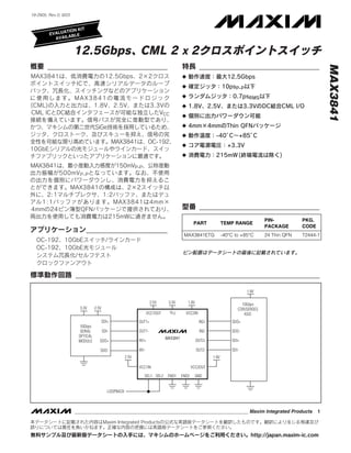
  • 1. 19-2905; Rev 0; 8/03 KIT ATION EVALU BLE AVAILA x MAX3841 _______________________________ _______________________________ ◆ ◆ ◆ ◆ ◆ ◆ ◆ ◆ ◆ _______________________________ PIN- PKG. PART TEMP RANGE PACKAGE CODE _____________________ MAX3841ETG -40°C to +85°C 24 Thin QFN T2444-1 _______________________________________________________________ 1.8V 2.5V 3.3V 1.8V 10Gbps 3.3V 2.5V CDR/SERDES VCC1OUT VCC VCC2IN ASIC SDI+ OUT1+ IN2+ SDO+ 10Gbps SERIAL SDI- OUT1- IN2- SDO- OPTICAL MAX3841 MODULE SDO+ IN1+ OUT2+ SDI+ SDO- IN1- OUT2- SDI- 2.5V 1.8V VCC1IN VCC2OUT SEL1 SEL2 ENO1 ENO2 GND LOOPBACK ________________________________________________________________ Maxim Integrated Products 1
  • 2. x ABSOLUTE MAXIMUM RATINGS MAX3841 Supply Voltage, VCC..............................................-0.5V to +4.0V Continuous Power Dissipation (TA = +85°C) CML Supply Voltage (VCC_IN, VCC_OUT)...........-0.5V to +4.0V 24-Pin Thin QFN (derate 20.8mW/°C Continuous Output Current (OUT1±, OUT2±)...................±25mA above +85°C).............................................................1352mW CML Input Voltage (IN1±, IN2±)...........-0.5V to (VCC_IN + 0.5V) Operating Temperature Range ...........................-40°C to +85°C LVCMOS Input Voltage (SEL1, SEL2, Storage Temperature Range .............................-55°C to +150°C ENO1, ENO2) .........................................-0.5V to (VCC + 0.5V) Lead Temperature (soldering, 10s) .................................+300°C Stresses beyond those listed under “Absolute Maximum Ratings” may cause permanent damage to the device. These are stress ratings only, and functional operation of the device at these or any other conditions beyond those indicated in the operational sections of the specifications is not implied. Exposure to absolute maximum rating conditions for extended periods may affect device reliability. ELECTRICAL CHARACTERISTICS (VCC = +3.0V to +3.6V, VCC_IN = +1.71V to VCC, VCC_OUT = +1.71V to VCC, TA = -40°C to +85°C. Typical values are at VCC = +3.3V, VCC_IN = VCC_OUT = 1.8V, TA = +25°C, unless otherwise noted.) PARAMETER SYMBOL CONDITIONS MIN TYP MAX UNITS Core Supply Current ICC Excluding CML termination currents 65 90 mA Data Rate (Note 1) 0 12.5 Gbps CML Input Differential VIN AC-coupled or DC-coupled (Note 2) 150 1200 mVP-P CML Input Common Mode DC-coupled VCC_IN - 0.3 VCC_IN V CML Input Termination Single ended 42.5 50 57.5 Ω CML Input Return Loss Up to 10GHz 12 dB CML Output Differential VOUT (Note 2) 400 500 600 mVP-P CML Output Termination Single ended 42.5 50 57.5 Ω CML Output Transition Time tR, tF 20% to 80% (Notes 1, 3) 30 ps Deterministic Jitter (Notes 1, 4) 10 psP-P Random Jitter VIN = 150mVP-P (Notes 1, 5) 0.3 0.7 psRMS Propagation Delay Any input to output (Note 1) 100 140 ps Channel-to-Channel Skew (Note 1) 12 ps Output Duty-Cycle Skew 50% input duty cycle (Notes 1, 3) 8 ps LVCMOS Input Current IIH, IIL -10 +10 µA LVCMOS Input High Voltage VIH 1.7 V Note 1: Guaranteed by design and characterization. Note 2: Differential swing is defined as VIN = (IN_+) - (IN_-) and VOUT = (OUT_+) - (OUT_-). See Figure 1. Note 3: Measured using a 0000011111 pattern at 12.5Gbps, and VIN = 400mVP-P differential. Note 4: Measured at 9.953Gbps using a pattern of 100 ones, 27 - 1 PRBS, 100 zeros, 27 - 1 PRBS, and at 12.5Gbps using a ±K28.5 pattern. VCC_IN = VCC_OUT = 1.8V, and VIN = 400mVP-P differential. Note 5: Refer to Maxim application note HFAN-04.5.1: Measuring Random Jitter on a Digital Sampling Oscilloscope. 2 _______________________________________________________________________________________
  • 3. x MAX3841 _______________________________________________________________ (VCC = 3.3V, VCC_IN, VCC_OUT = 1.8V, VIN = 500mVP-P, TA = +25°C, unless otherwise noted.) CORE SUPPLY CURRENT vs. TEMPERATURE SUPPLY CURRENT vs. TEMPERATURE OUTPUT EYE DIAGRAM (EXCLUDES CML I/O CURRENTS) (CORE PLUS CML I/O CURRENTS) (12.5Gbps, 223 - 1 PRBS) MAX3841 toc03 140 140 MAX3841 toc02 MAX3841 toc01 130 130 120 120 2 OUTPUTS ENABLE SUPPLY CURRENT (mA) SUPPLY CURRENT (mA) 110 0 OUTPUTS ENABLE 110 1 OUTPUT ENABLE 100 1 OUTPUT ENABLE 100 90 90 0 OUTPUTS ENABLE 60mV/div 80 2 OUTPUTS ENABLE 80 70 70 60 60 50 50 CML INPUTS AND OUTPUTS AC-COUPLED 40 40 -40 -15 10 35 60 85 -40 -15 10 35 60 85 14ps/div TEMPERATURE (°C) TEMPERATURE (°C) OUTPUT EYE DIAGRAM OUTPUT EYE DIAGRAM OUTPUT EYE DIAGRAM (10.7Gbps, 223 - 1 PRBS) (6.25Gbps, 223 - 1 PRBS) (622Mbps, 223 - 1 PRBS) MAX3841 toc04 MAX3841 toc05 MAX3841 toc06 60mV/div 60mV/div 60mV/div 16ps/div 28ps/div 270ps/div DETERMINISTIC JITTER DIFFERENTIAL OUTPUT SWING vs. TEMPERATURE vs. TEMPERATURE PROPAGATION DELAY MAX3841 toc09 16 550 MAX3841 toc08 MAX3841 toc07 7 540 14 2 - 1 PRBS + 100CIDs AT 10.7Gbps DIFFERENTIAL OUTPUT (mVP-P) 530 DETERMINISTIC JITTER (ps) 12 IN1 520 10 510 8 500 490 6 480 4 OUT1 470 2 460 ±K28.5 AT 12.5Gbps 0 450 -40 -15 10 35 60 85 -40 -15 10 35 60 85 100ps/div TEMPERATURE (°C) TEMPERATURE (°C) _______________________________________________________________________________________ 3
  • 4. x MAX3841 ___________________________________________________________________ PIN NAME FUNCTION 1, 12 VCC +3.3V Core Supply Voltage 2, 5 VCC1IN Supply Voltage for CML Input IN1. Connect to 1.8V, 2.5V, or 3.3V. 3 IN1+ Positive Serial Data Input 1, CML 4 IN1- Negative Serial Data Input 1, CML 6 SEL1 Output 1 Select, LVCMOS Input. See Table 1. 7 SEL2 Output 2 Select, LVCMOS Input. See Table 1. 8, 11 VCC2IN Supply Voltage for CML Input IN2. Connect to 1.8V, 2.5V, or 3.3V. 9 IN2+ Positive Serial Data Input 2, CML 10 IN2- Negative Serial Data Input 2, CML 13, 24 GND Supply Ground 14, 17 VCC1OUT Supply Voltage for CML Output OUT1. Connect to 1.8V, 2.5V, or 3.3V. 15 OUT1- Negative Serial Data Output 1, CML 16 OUT1+ Positive Serial Data Output 1, CML 18 ENO1 Output 1 Enable, LVCMOS Input. See Table 1. 19 ENO2 Output 2 Enable, LVCMOS Input. See Table 1. 20, 23 VCC2OUT Supply Voltage for CML Output OUT2. Connect to 1.8V, 2.5V, or 3.3V. 21 OUT2- Negative Serial Data Output 2, CML 22 OUT2+ Positive Serial Data Output 2, CML Ground. The exposed pad must be soldered to the circuit board ground for proper thermal and EP Exposed Pad electrical performance. _______________________________ 2 IN1 CML 1 2 CML OUT1 0 ENO1 SEL1 2 IN2 CML 1 2 CML OUT2 0 Ω Ω ENO2 MAX3841 SEL2 4 _______________________________________________________________________________________
  • 5. x MAX3841 V- 75mV MIN ENO1 ENO2 SEL1 SEL2 OUT1 OUT2 600mV MAX 0 0 0 0 IN2 IN1 0 0 0 1 IN2 IN2 V+ 0 0 1 0 IN1 IN1 0 0 1 1 IN1 IN2 150mV 1 1 X X Disabled Disabled MIN (V+) - (V-) 1200mV MAX _________________ VCC_IN 50Ω 50Ω IN_+ IN_- MAX3841 VCC_OUT 50Ω 50Ω OUT_+ Ω OUT_- MAX3841 _______________________________________________________________________________________ 5
  • 6. x MAX3841 ____________________________ __________________________ TRANSISTOR COUNT: 950 VCC2OUT VCC2OUT TOP VIEW PROCESS: SiGe BiCMOS OUT2+ OUT2- ENO2 GND 24 23 22 21 20 19 VCC 1 18 ENO1 VCC1IN 2 17 VCC1OUT IN1+ 3 16 OUT1+ IN1- 4 MAX3841 15 OUT1- VCC1IN 5 14 VCC1OUT SEL1 6 13 GND 7 8 9 10 11 12 SEL2 VCC2IN IN2+ IN2- VCC2IN VCC THIN QFN* *THE EXPOSED PAD OF THE QFN PACKAGE MUST BE SOLDERED TO GROUND FOR PROPER THERMAL AND ELECTRICAL OPERATION. 6 _______________________________________________________________________________________
  • 7. x MAX3841 ________________________________________________________________________ http://japan.maxim-ic.com/packages 24L QFN THIN.EPS PACKAGE OUTLINE 12,16,20,24L QFN THIN, 4x4x0.8 mm 1 21-0139 B 2 _______________________________________________________________________________________ 7
  • 8. x MAX3841 ___________________________________________________________________ http://japan.maxim-ic.com/packages PACKAGE OUTLINE 12,16,20,24L QFN THIN, 4x4x0.8 mm 2 21-0139 B 2 Maxim Integrated Products, 120 San Gabriel Drive, Sunnyvale, CA 94086 (408) 737-7600 __________________ 8 © 2003 Maxim Integrated Products is a registered trademark of Maxim Integrated Products.