Synchronous Buck Converter using LTspice
•Télécharger en tant que PPTX, PDF•
1 j'aime•5,425 vues

Synchronous Buck Converter using LTspice

Recommandé
Contenu connexe
Tendances
Tendances (20)
En vedette
En vedette (13)
Similaire à Synchronous Buck Converter using LTspice
Similaire à Synchronous Buck Converter using LTspice (20)
Plus de Tsuyoshi Horigome
Plus de Tsuyoshi Horigome (20)
Dernier
Dernier (20)
Synchronous Buck Converter using LTspice
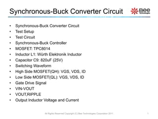
- 1. Synchronous-Buck Converter Circuit • Synchronous-Buck Converter Circuit • Test Setup • Test Circuit • Synchronous-Buck Controller • MOSFET: TPC8014 • Inductor L1: Würth Elektronik Inductor • Capacitor C9: 820uF (25V) • Switching Waveform • High Side MOSFET(QH): VGS, VDS, ID • Low Side MOSFET(QL): VGS, VDS, ID • Gate Drive Signal • VIN-VOUT • VOUT,RIPPLE • Output Inductor Voltage and Current All Rights Reserved Copyright (C) Bee Technologies Corporation 2011 1
- 2. Synchronous-Buck Converter Circuit Duty Cycle (D) ≈ Vin/Vout, D = 0.368 All Rights Reserved Copyright (C) Bee Technologies Corporation 2011 2
- 3. Test Setup Power Supply: Measurement Waveform VCC 12V VIN 5V Test Circuit All Rights Reserved Copyright (C) Bee Technologies Corporation 2011 3
- 4. Test Circuit Schematic Synchronous-Buck Converter using TPS5618 controller from Texas Instruments All Rights Reserved Copyright (C) Bee Technologies Corporation 2011 4
- 5. Test Circuit (Breadboard) Q1 Q2 Controller All Rights Reserved Copyright (C) Bee Technologies Corporation 2011 5
- 6. Test Circuit (Top View) L1 C9 C10 Controller All Rights Reserved Copyright (C) Bee Technologies Corporation 2011 6
- 7. Synchronous-Buck Controller (1/2) Synchronous-Buck Controller Circuit with IC Synchronous-Buck Controller Block Model TPS5618 from Texas Instruments (Open Loop Setting) HIDR High side gate driver Low side gate driver LODR • The Syn-Buck_Ctrl is a block model that generates gate drive pulse signal to control MOSFET switches of the Synchronous-Buck Converter. The duty cycle, switching frequency, and the switching dead-time are input into the model to match the real circuit. All Rights Reserved Copyright (C) Bee Technologies Corporation 2011 7
- 8. Synchronous-Buck Controller (2/2) Parameters • FREQ = Switching frequency, set to match the measurement switching frequency. PARAMETERS: • D = Duty Cycle, calculated by D≈VOUT/VIN • FREQ = 152kHz D = 0.36 DHDR1 RHDR1 tdly = HDR and LDR dead-time, the tdly is U1 Dclmp 0.01 tdly = 80n AND2_ABM N7 set to match the measurement dead time Rdly 1 N4 N5 N6 HDR value. Dclmp RHDR2 CHDR Dead-time, the time 1k Cdly 1 VOH = 12 DHDR2 0.01 1n when QH and QL Pulse {tdly /1k} VOL = 0 0 are both off Control 0 Signal 1/frequency U5 U2 INV_ABM AND2_ABM N1 N2 Rdly 2 N3 LDR VOH = 1.709 VOL = 0 1k V1 Cdly 2 VOH = 8 {tdly /1k} VOL = 0 TD = {1/FREQ} TR = 1n 0 TF = 1n Dead-time 0 V1 = 0 V2 = 1.709 generator PW = {D/FREQ} PER = {1/FREQ} The Syn-Buck_Ctrl Equivalent Circuit Gate drive signal (measurement) All Rights Reserved Copyright (C) Bee Technologies Corporation 2011 8
- 9. MOSFET: TPC8014 (1/2) *$ *PART NUMBER: TPC8014 *MANUFACTURER: TOSHIBA *VDSS=30V, ID=11A *All Rights Reserved Copyright (c) Bee Technologies Inc. 2011 .SUBCKT TPC8014 1 2 3 4 5 6 7 8 X_U1 6 4 3 MTPC8014_p X_U2 4 3 DZTPC8014 X_U3 3 6 DTPC8014_p R_R1 1 3 0.01m R_R2 2 3 0.01m R_R5 5 6 0.01m R_R7 7 6 0.01m Device mounted on an epoxy board R_R8 8 6 0.01m .ENDS *$ TPC8014 LTSpice Symbol All Rights Reserved Copyright (C) Bee Technologies Corporation 2011 9
- 10. MOSFET: TPC8014 (2/2) *$ *$ .SUBCKT DTPC8014_p A K .SUBCKT MTPC8014_p D G S R_R2 5 6 100 CGD 1 G 1.7n R_R1 3 4 1 R1 1 G 10MEG C_C1 5 6 195p S1 1 D G D SMOD1 E_E1 5 K 3 4 1 S_S1 6 K 4 K _S1 D1 2 D DGD RS_S1 4 K 1G R2 D 2 10MEG .MODEL _S1 VSWITCH S2 2 G D G SMOD1 + Roff=50MEG Ron=100m Voff=90mV Von=100mV M1 D G S S MTPC8014 G_G1 K A VALUE { V(3,4)-V(5,6) } D_D1 2 K DTPC8014 .MODEL SMOD1 VSWITCH D_D2 4 K DTPC8014 + VON=0V VOFF=-10mV RON=1m ROFF=1E12 F_F1 K 3 VF_F1 1 .MODEL DGD D (CJO=0.950E-9 M=.52396 VJ=.54785) VF_F1 A 2 0V .MODEL MTPC8014 NMOS .MODEL DTPC8014 D + LEVEL=3 L=720.00E-9 W=.45 KP=66.000E-6 RS=1.0000E-3 + IS=824.87E-12 N=1.2770 RS=6.2420E-3 IKF=7.3139 + CJO=3.0000E-12 BV=60 IBV=100.00E-6 TT=24.062E-9 + RD=6.8436E-3 VTO=2.3063 RDS=3.0000E6 TOX=40.000E-9 .ENDS + CGSO=2.7726E-9 CGDO=1E-12 RG=22.95 *$ + CBD=342.86E-12 MJ=.70573 PB=.3905 .subckt DZTPC8014 1 2 + RB=1 N=5 IS=1E-15 GAMMA=0 KAPPA=0 ETA=0.5m D2 1 3 DZ2 D1 2 3 DZ1 .ENDS .model DZ1 D *$ + IS=0.01p N=0.1 ISR=0 + CJO=3E-12 BV=22.423 IBV=0.001 RS=0 .model DZ2 D + IS=0.01p N=0.1 ISR=0 + CJO=3E-12 BV=22.423 IBV=0.001 RS=411.11 .ENDS *$ All Rights Reserved Copyright (C) Bee Technologies Corporation 2011 10
- 11. Inductor L1: Würth Elektronik Inductor *$ *PART NUMBER: L7447140 *MANUFACTURER: Würth Elektronik *All Rights Reserved Copyright (c) Bee Technologies Inc. 2011 .SUBCKT L7447140 1 2 R_RS 1 N1 10.366m L_L1 N1 2 4.84796uH C_C1 N1 2 0.357pF R_R1 N1 2 15.3375k .ENDS *$ Würth Elektronik Inductor part no. 7447140 LTSpice Symbol All Rights Reserved Copyright (C) Bee Technologies Corporation 2011 11
- 12. Capacitor C9: 820uF (25V) *$ *PART NUMBER: EEUFM1E821L *MANUFACTURER: Panasonic *CAP=820uF, Vmax=25V *All Rights Reserved Copyright (C) Bee Technologies Inc. 2011 .SUBCKT C820U 1 2 L_L1 1 N1 8.16935nH C_C1 N1 N2 812.73uF R_R1 N2 2 15.695m .ENDS *$ Capacitor 820uF (25V) LTSpice Symbol All Rights Reserved Copyright (C) Bee Technologies Corporation 2011 12
- 13. Switching Waveform Measurement Simulation VDS(Q1) VDS(Q1) I(L1) I(L1) V(Vout) V(Vout) All Rights Reserved Copyright (C) Bee Technologies Corporation 2011 13
- 14. High Side MOSFET(QH): VGS, VDS, ID Measurement Simulation VGS(Q1) VGS(Q1) VDS(Q1) VDS(Q1) ID(Q1) ID(Q1) All Rights Reserved Copyright (C) Bee Technologies Corporation 2011 14
- 15. Low Side MOSFET(QL): VGS, VDS, ID Measurement Simulation VGS(Q2) VGS(Q2) VDS(Q2) VDS(Q2) ID(Q2) ID(Q2) All Rights Reserved Copyright (C) Bee Technologies Corporation 2011 15
- 16. Gate Drive Signal Measurement Simulation VGS(Q1) VGS(Q1) VGS(Q2) VGS(Q2) All Rights Reserved Copyright (C) Bee Technologies Corporation 2011 16
- 17. VIN – VOUT Measurement Simulation VIN VIN VOUT VOUT All Rights Reserved Copyright (C) Bee Technologies Corporation 2011 17
- 18. VOUT,RIPPLE Measurement Simulation VOUT,RIPPLE VOUT,RIPPLE All Rights Reserved Copyright (C) Bee Technologies Corporation 2011 18
- 19. Output Inductor Voltage and Current Measurement Simulation V(L) V(L) I(L) I(L) All Rights Reserved Copyright (C) Bee Technologies Corporation 2011 19