SlideShare une entreprise Scribd logo
1  sur  27
CPLDs
• The block diagram at
  right for the Cypress
  Semiconductor CPLD
  (Ultra37128) illustrates
  the general architecture
  of CPLDs


                                                Programmable
                                                Logic Devices
                                                   (FPLDs)


                                    SPLDs          CPLDs            FPGAs
                                 (e.g., PALs)


                                                                1
Cypress Ultra 37000 Family
• In-system reprogrammable
  CMOS CPLDs
  – JTAG interface for
    reconfigurability
  – Design changes do not cause
    pinout changes
  – Design changes do not cause
    timing changes
• High density
  – 32 to 512 macrocells
  – 32 to 264 I/O pins
  – Five dedicated inputs including
    four clock pins


                                      2
Cypress Ultra 37000 Family
• Characteristics of devices in the Ultra 37000 Family


                                                         3
CPLDs
• Complex Programmable Logic Devices
  – Contain from 10-1000 macrocells
  – Each macrocell is equivalent to around 20 gates
  – Support up to 200 I/O pins
• The key resource in a CPLD is the programmable
  interconnect
  – Tradeoff between space for macrocells and space for
    interconnect
  – Careful design will limit the connections between
    macrocells

                                                      Programmable
                                                      Logic Devices
                                                         (FPLDs)


                                          SPLDs          CPLDs            FPGAs
                                       (e.g., PALs)


                                                                      4
CPLD Architecture
• Complexity of CPLD is between FPGA and SPLD


           LAB – Logic Array Block / uses PALs
          PIA – Programmable Interconnect Array   5
CPLD Architecture
   • Example Logic Array Block


                                         Extra function (e.g., g,
                                         h) i/ps for OR term               2:1 Mux


                                                                    D-FF


                                 PLA-like AND array
Literal inputs (e.g., a, b, c)
                                                                            6
Programmable Interconnect Array
• Consists of connectors that run throughout the CPLD
  to connect the macrocells in each LAB
• The PIA also connects the AND gate and other
  elements of the macrocells


                                                        7
CPLD/FPGA Vendors
• The main vendors


                              8
CPLD Families
• Identical individual PLD blocks (Xilinx “FBs”) replicated
  in different family members
  – Different number of PLD blocks
  – Different number of I/O pins


                                                 Xilinx
                                                 XC9500
                                                 CPLD
                                                 Series


                                                          9
Typical CPLD Packages
• CPLDs are made using 2 to 64 SPLDs
• Packages use 44-pins to over 200-pins (or more)


                                                    10
Typical CPLD Packages
• QFP = Quad Flat Package
– A QFP is an IC package with leads extending from each of
  the four sides.
– It is used primarily for surface mounting, no socketing
• TQFP = Thin Quad Flat Package
• PQFP = Plastic Quad Flat Package
• VQFP = Very small Quad Flat Package

• PLCC = Plastic Leaded Chip Carrier
– A package related to QFP
– Similar but has pins with larger distance, curved up
  underneath a thicker body to simplify socketing

                                                         11
CPLD Package Types
• CSP = Chip Scale Package
  – IC package with an area no greater than 1.2 times that
    of the die


• BGA = Ball Grid Array
  – A type of surface-mount packaging used for ICs
  – Pins are replaced by balls of solder stuck to the bottom
    of the package
  – The device is placed on a PCB that carries copper pads
    in a pattern that matches the solder balls
  – The assembly is then heated causing the solder balls to
    melt


                                                             12
CPLD Families
• Many CPLDs have fewer
  I/O pins than macrocells
  – “Buried” Macrocells – provide
    needed logic terms internally
    but these outputs are not
    connected externally
  – IC package size dictates
    number of I/O pins but not
    the total number of
    macrocells
  – Typical CPLD families have devices with differing
    resources in the same IC package


                                                        13
Xilinx CPLDs
• Notice overlap in resource availability in a particular
  package.


                                                            14
XC9572 CPLD Datasheet
• XC9572 CPLD from Xilinx
• 7.5 ns pin-to-pin logic
  delays on all pins
• 72 macrocells with 1,600
  usable gates
• Up to 72 user I/O pins
• Four 36V18 Function
  Blocks
• Available in 44-pin PLCC,
  84-pin PLCC, 100-pin
  PQFP and 100-pin TQFP
  packages

                                15
XC9572 CPLD Packages
• XC9572 pinout for the 84-pin PLCC package and
  photo of the 100-pin TQFP package

      84-pin PLCC                 100-pin TQFP
         (pin 1)


                                                  16
XC9572 CPLD Part Numbers
• The part number for Xilinx CPLD devices includes
  information as follows:


                                                     17
XC9500 CPLD Block Diagram
• The XC9500 CPLD
  family provides
  advanced in-system
  programming and test
  capabilities for high
  performance, general
  purpose logic
  integration.
• All devices are in-
  system programmable
  for a minimum of
  10,000 program/erase
  cycles.

                                 18
9500-Family Function Blocks (FBs)
• 18 macrocells per FB
• 36 inputs per FB (partitioning challenge, but also
  reason for relatively compact size of FBs)
• Macrocell outputs can go to I/O cells or back into
  switch matrix to be routed to this or other FBs


                                                       19
9500-Series Macrocell
 • 18 macrocells per Function Block

                       Set control

        Programmable inversion
            or XOR product term


            Up to 5 product terms

Global clock or product-term clock


                    Reset control


                       OE control

                                        20
9500-Series Product-Term Allocator
  • Share terms from above and below


programmable
steering
elements


                                       21
XC9500 Family
• An I/O block is composed of
  input buffer, output buffer,
  multiplexer for the output
  control and grounding control
• Slew rate control is used to
  smooth the rising and the falling
  edges of the output pulse.
• Grounding control is used to
  make the input/output pin (I/O)
  an earth ground (noise
  suppression).
• Each input/output pin can handle a 24-mA current.


                                                      22
9500-Series I/O Block
• OE Multiplexer (OE
  MUX) controls an output
  enable or stop.
• It is controlled by the
  signal from the macrocell
  or the signal from the
  GTS (Global Three-State
  control) pin.
• There are four
  GTS in XC95216
  and XC95288
  two in the
  others.

                                   23
XC95108 CPLD Datasheet
• XC95108 shares the
  characteristics of all other
  XC9500 series devices
• 108 macrocells with 2400
  usable gates
• Up to 108 user I/O pins
• Six 36V18 Function Blocks
• 10,000 program/erase
  cycles
• Available in 84-pin PLCC,
  100-pin PQFP, 100-pin
  TQFP and 160-pin PQFP
  packages
                                 24
XC95108 CPLD Datasheet
• XC95108 block diagram
  is similar to all of the
  others in the XC9500
  family


                                 25
Switch Matrix for XC95108
• Could be anything from a limited set of multiplexers to
  a full crossbar
  – Multiplexer -- small, fast, but difficult fitting
  – Crossbar -- easy fitting but large and slow


                                                        26
Problems with CPLDs
• Pin locking
  – Small changes, and certainly large ones, can cause the
    fitter to pick a different allocation of I/O blocks and pinout
  – Locking too early may make the resulting circuit slower
    or not fit at all
• Running out of resources
  – Design may “blow up” if it doesn’t all fit on a single
    device
  – On-chip interconnect resources are much richer than off-
    chip
  – Larger devices are exponentially more expensive


                                                                27

Contenu connexe

Tendances

Programmable peripheral interface 8255
Programmable peripheral interface 8255Programmable peripheral interface 8255
Programmable peripheral interface 8255Marajulislam3
 
Introduction state machine
Introduction state machineIntroduction state machine
Introduction state machineShreyans Pathak
 
Complex Programmable Logic Device (CPLD) Architecture and Its Applications
Complex Programmable Logic Device (CPLD) Architecture and Its ApplicationsComplex Programmable Logic Device (CPLD) Architecture and Its Applications
Complex Programmable Logic Device (CPLD) Architecture and Its Applicationselprocus
 
synchronous state machine design
synchronous state machine designsynchronous state machine design
synchronous state machine designAdarsh Patel
 
Addressing modes of 8051
Addressing modes of 8051Addressing modes of 8051
Addressing modes of 8051SARITHA REDDY
 
Programmable Logic Devices Plds
Programmable Logic Devices PldsProgrammable Logic Devices Plds
Programmable Logic Devices PldsGaditek
 
Verilog Tutorial - Verilog HDL Tutorial with Examples
Verilog Tutorial - Verilog HDL Tutorial with ExamplesVerilog Tutorial - Verilog HDL Tutorial with Examples
Verilog Tutorial - Verilog HDL Tutorial with ExamplesE2MATRIX
 
Digital electronics logic families
Digital electronics logic familiesDigital electronics logic families
Digital electronics logic familiesBLESSINAR0
 
MOSFET Small signal model
MOSFET Small signal modelMOSFET Small signal model
MOSFET Small signal modelTeam-VLSI-ITMU
 
8085 microprocessor ramesh gaonkar
8085 microprocessor   ramesh gaonkar8085 microprocessor   ramesh gaonkar
8085 microprocessor ramesh gaonkarSAQUIB AHMAD
 
Power mosfet characteristics
Power mosfet characteristicsPower mosfet characteristics
Power mosfet characteristicssanu singh
 
Interfacing of io device to 8085
Interfacing of io device to 8085Interfacing of io device to 8085
Interfacing of io device to 8085Nitin Ahire
 
Memory & I/O interfacing
Memory & I/O  interfacingMemory & I/O  interfacing
Memory & I/O interfacingdeval patel
 
Programmable array logic
Programmable array logicProgrammable array logic
Programmable array logicGaditek
 

Tendances (20)

Programmable peripheral interface 8255
Programmable peripheral interface 8255Programmable peripheral interface 8255
Programmable peripheral interface 8255
 
Introduction state machine
Introduction state machineIntroduction state machine
Introduction state machine
 
Complex Programmable Logic Device (CPLD) Architecture and Its Applications
Complex Programmable Logic Device (CPLD) Architecture and Its ApplicationsComplex Programmable Logic Device (CPLD) Architecture and Its Applications
Complex Programmable Logic Device (CPLD) Architecture and Its Applications
 
synchronous state machine design
synchronous state machine designsynchronous state machine design
synchronous state machine design
 
8251 USART
8251 USART8251 USART
8251 USART
 
Cpld fpga
Cpld fpgaCpld fpga
Cpld fpga
 
E.s unit 6
E.s unit 6E.s unit 6
E.s unit 6
 
Sample and hold circuit
Sample and hold circuitSample and hold circuit
Sample and hold circuit
 
Sensistor
SensistorSensistor
Sensistor
 
Addressing modes of 8051
Addressing modes of 8051Addressing modes of 8051
Addressing modes of 8051
 
Programmable Logic Devices Plds
Programmable Logic Devices PldsProgrammable Logic Devices Plds
Programmable Logic Devices Plds
 
Verilog Tutorial - Verilog HDL Tutorial with Examples
Verilog Tutorial - Verilog HDL Tutorial with ExamplesVerilog Tutorial - Verilog HDL Tutorial with Examples
Verilog Tutorial - Verilog HDL Tutorial with Examples
 
Digital electronics logic families
Digital electronics logic familiesDigital electronics logic families
Digital electronics logic families
 
MOSFET Small signal model
MOSFET Small signal modelMOSFET Small signal model
MOSFET Small signal model
 
8085 microprocessor ramesh gaonkar
8085 microprocessor   ramesh gaonkar8085 microprocessor   ramesh gaonkar
8085 microprocessor ramesh gaonkar
 
Power mosfet characteristics
Power mosfet characteristicsPower mosfet characteristics
Power mosfet characteristics
 
Interfacing of io device to 8085
Interfacing of io device to 8085Interfacing of io device to 8085
Interfacing of io device to 8085
 
Vlsi Synthesis
Vlsi SynthesisVlsi Synthesis
Vlsi Synthesis
 
Memory & I/O interfacing
Memory & I/O  interfacingMemory & I/O  interfacing
Memory & I/O interfacing
 
Programmable array logic
Programmable array logicProgrammable array logic
Programmable array logic
 

Similaire à CPLDs

Similaire à CPLDs (20)

PLD's.pptx
PLD's.pptxPLD's.pptx
PLD's.pptx
 
1.CPLD SPLD.pdf
1.CPLD SPLD.pdf1.CPLD SPLD.pdf
1.CPLD SPLD.pdf
 
Fpga &;cpld(by alok singh)
Fpga &;cpld(by alok singh)Fpga &;cpld(by alok singh)
Fpga &;cpld(by alok singh)
 
Lecture syn 024.cpld-fpga
Lecture syn 024.cpld-fpgaLecture syn 024.cpld-fpga
Lecture syn 024.cpld-fpga
 
Cpld and fpga mod vi
Cpld and fpga   mod viCpld and fpga   mod vi
Cpld and fpga mod vi
 
Pld dp
Pld dpPld dp
Pld dp
 
SoC FPGA Technology
SoC FPGA TechnologySoC FPGA Technology
SoC FPGA Technology
 
module7.pptx
module7.pptxmodule7.pptx
module7.pptx
 
CPLD & FPLD
CPLD & FPLDCPLD & FPLD
CPLD & FPLD
 
CPLDs
CPLDsCPLDs
CPLDs
 
CPLDs
CPLDsCPLDs
CPLDs
 
L12_PROGRAMMABLE+LOGIC+DEVICES+(PLD).ppt
L12_PROGRAMMABLE+LOGIC+DEVICES+(PLD).pptL12_PROGRAMMABLE+LOGIC+DEVICES+(PLD).ppt
L12_PROGRAMMABLE+LOGIC+DEVICES+(PLD).ppt
 
L12 programmable+logic+devices+(pld)
L12 programmable+logic+devices+(pld)L12 programmable+logic+devices+(pld)
L12 programmable+logic+devices+(pld)
 
1. FPGA architectures.pdf
1. FPGA architectures.pdf1. FPGA architectures.pdf
1. FPGA architectures.pdf
 
Programable logic devices (1)
Programable logic devices (1)Programable logic devices (1)
Programable logic devices (1)
 
Fpga optimus main_print
Fpga optimus  main_printFpga optimus  main_print
Fpga optimus main_print
 
Evolution of logic devices from SSIs to FPGAs
Evolution of logic devices from SSIs to FPGAsEvolution of logic devices from SSIs to FPGAs
Evolution of logic devices from SSIs to FPGAs
 
Fpga & VHDL
Fpga & VHDLFpga & VHDL
Fpga & VHDL
 
Lab9500
Lab9500Lab9500
Lab9500
 
Dr.D.RUKMANIDEVI PPT.ppt
Dr.D.RUKMANIDEVI PPT.pptDr.D.RUKMANIDEVI PPT.ppt
Dr.D.RUKMANIDEVI PPT.ppt
 

Plus de Abhilash Nair

Sequential Circuits - Flip Flops
Sequential Circuits - Flip FlopsSequential Circuits - Flip Flops
Sequential Circuits - Flip FlopsAbhilash Nair
 
Designing Clocked Synchronous State Machine
Designing Clocked Synchronous State MachineDesigning Clocked Synchronous State Machine
Designing Clocked Synchronous State MachineAbhilash Nair
 
VHDL - Enumerated Types (Part 3)
VHDL - Enumerated Types (Part 3)VHDL - Enumerated Types (Part 3)
VHDL - Enumerated Types (Part 3)Abhilash Nair
 
Introduction to VHDL - Part 1
Introduction to VHDL - Part 1Introduction to VHDL - Part 1
Introduction to VHDL - Part 1Abhilash Nair
 
Feedback Sequential Circuits
Feedback Sequential CircuitsFeedback Sequential Circuits
Feedback Sequential CircuitsAbhilash Nair
 
Designing State Machine
Designing State MachineDesigning State Machine
Designing State MachineAbhilash Nair
 
State Machine Design and Synthesis
State Machine Design and SynthesisState Machine Design and Synthesis
State Machine Design and SynthesisAbhilash Nair
 
Synchronous design process
Synchronous design processSynchronous design process
Synchronous design processAbhilash Nair
 
Analysis of state machines & Conversion of models
Analysis of state machines & Conversion of modelsAnalysis of state machines & Conversion of models
Analysis of state machines & Conversion of modelsAbhilash Nair
 
Analysis of state machines
Analysis of state machinesAnalysis of state machines
Analysis of state machinesAbhilash Nair
 
Sequential Circuits - Flip Flops (Part 2)
Sequential Circuits - Flip Flops (Part 2)Sequential Circuits - Flip Flops (Part 2)
Sequential Circuits - Flip Flops (Part 2)Abhilash Nair
 
Sequential Circuits - Flip Flops (Part 1)
Sequential Circuits - Flip Flops (Part 1)Sequential Circuits - Flip Flops (Part 1)
Sequential Circuits - Flip Flops (Part 1)Abhilash Nair
 
Static and Dynamic Read/Write memories
Static and Dynamic Read/Write memoriesStatic and Dynamic Read/Write memories
Static and Dynamic Read/Write memoriesAbhilash Nair
 
Documentation Standards of an IC
Documentation Standards of an ICDocumentation Standards of an IC
Documentation Standards of an ICAbhilash Nair
 

Plus de Abhilash Nair (20)

Sequential Circuits - Flip Flops
Sequential Circuits - Flip FlopsSequential Circuits - Flip Flops
Sequential Circuits - Flip Flops
 
VHDL Part 4
VHDL Part 4VHDL Part 4
VHDL Part 4
 
Designing Clocked Synchronous State Machine
Designing Clocked Synchronous State MachineDesigning Clocked Synchronous State Machine
Designing Clocked Synchronous State Machine
 
MSI Shift Registers
MSI Shift RegistersMSI Shift Registers
MSI Shift Registers
 
VHDL - Enumerated Types (Part 3)
VHDL - Enumerated Types (Part 3)VHDL - Enumerated Types (Part 3)
VHDL - Enumerated Types (Part 3)
 
VHDL - Part 2
VHDL - Part 2VHDL - Part 2
VHDL - Part 2
 
Introduction to VHDL - Part 1
Introduction to VHDL - Part 1Introduction to VHDL - Part 1
Introduction to VHDL - Part 1
 
Feedback Sequential Circuits
Feedback Sequential CircuitsFeedback Sequential Circuits
Feedback Sequential Circuits
 
Designing State Machine
Designing State MachineDesigning State Machine
Designing State Machine
 
State Machine Design and Synthesis
State Machine Design and SynthesisState Machine Design and Synthesis
State Machine Design and Synthesis
 
Synchronous design process
Synchronous design processSynchronous design process
Synchronous design process
 
Analysis of state machines & Conversion of models
Analysis of state machines & Conversion of modelsAnalysis of state machines & Conversion of models
Analysis of state machines & Conversion of models
 
Analysis of state machines
Analysis of state machinesAnalysis of state machines
Analysis of state machines
 
Sequential Circuits - Flip Flops (Part 2)
Sequential Circuits - Flip Flops (Part 2)Sequential Circuits - Flip Flops (Part 2)
Sequential Circuits - Flip Flops (Part 2)
 
Sequential Circuits - Flip Flops (Part 1)
Sequential Circuits - Flip Flops (Part 1)Sequential Circuits - Flip Flops (Part 1)
Sequential Circuits - Flip Flops (Part 1)
 
FPGA
FPGAFPGA
FPGA
 
FPLDs
FPLDsFPLDs
FPLDs
 
Static and Dynamic Read/Write memories
Static and Dynamic Read/Write memoriesStatic and Dynamic Read/Write memories
Static and Dynamic Read/Write memories
 
Documentation Standards of an IC
Documentation Standards of an ICDocumentation Standards of an IC
Documentation Standards of an IC
 
Shift Registers
Shift RegistersShift Registers
Shift Registers
 

CPLDs

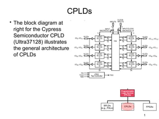
  • 1. CPLDs • The block diagram at right for the Cypress Semiconductor CPLD (Ultra37128) illustrates the general architecture of CPLDs Programmable Logic Devices (FPLDs) SPLDs CPLDs FPGAs (e.g., PALs) 1
  • 2. Cypress Ultra 37000 Family • In-system reprogrammable CMOS CPLDs – JTAG interface for reconfigurability – Design changes do not cause pinout changes – Design changes do not cause timing changes • High density – 32 to 512 macrocells – 32 to 264 I/O pins – Five dedicated inputs including four clock pins 2
  • 3. Cypress Ultra 37000 Family • Characteristics of devices in the Ultra 37000 Family 3
  • 4. CPLDs • Complex Programmable Logic Devices – Contain from 10-1000 macrocells – Each macrocell is equivalent to around 20 gates – Support up to 200 I/O pins • The key resource in a CPLD is the programmable interconnect – Tradeoff between space for macrocells and space for interconnect – Careful design will limit the connections between macrocells Programmable Logic Devices (FPLDs) SPLDs CPLDs FPGAs (e.g., PALs) 4
  • 5. CPLD Architecture • Complexity of CPLD is between FPGA and SPLD LAB – Logic Array Block / uses PALs PIA – Programmable Interconnect Array 5
  • 6. CPLD Architecture • Example Logic Array Block Extra function (e.g., g, h) i/ps for OR term 2:1 Mux D-FF PLA-like AND array Literal inputs (e.g., a, b, c) 6
  • 7. Programmable Interconnect Array • Consists of connectors that run throughout the CPLD to connect the macrocells in each LAB • The PIA also connects the AND gate and other elements of the macrocells 7
  • 8. CPLD/FPGA Vendors • The main vendors 8
  • 9. CPLD Families • Identical individual PLD blocks (Xilinx “FBs”) replicated in different family members – Different number of PLD blocks – Different number of I/O pins Xilinx XC9500 CPLD Series 9
  • 10. Typical CPLD Packages • CPLDs are made using 2 to 64 SPLDs • Packages use 44-pins to over 200-pins (or more) 10
  • 11. Typical CPLD Packages • QFP = Quad Flat Package – A QFP is an IC package with leads extending from each of the four sides. – It is used primarily for surface mounting, no socketing • TQFP = Thin Quad Flat Package • PQFP = Plastic Quad Flat Package • VQFP = Very small Quad Flat Package • PLCC = Plastic Leaded Chip Carrier – A package related to QFP – Similar but has pins with larger distance, curved up underneath a thicker body to simplify socketing 11
  • 12. CPLD Package Types • CSP = Chip Scale Package – IC package with an area no greater than 1.2 times that of the die • BGA = Ball Grid Array – A type of surface-mount packaging used for ICs – Pins are replaced by balls of solder stuck to the bottom of the package – The device is placed on a PCB that carries copper pads in a pattern that matches the solder balls – The assembly is then heated causing the solder balls to melt 12
  • 13. CPLD Families • Many CPLDs have fewer I/O pins than macrocells – “Buried” Macrocells – provide needed logic terms internally but these outputs are not connected externally – IC package size dictates number of I/O pins but not the total number of macrocells – Typical CPLD families have devices with differing resources in the same IC package 13
  • 14. Xilinx CPLDs • Notice overlap in resource availability in a particular package. 14
  • 15. XC9572 CPLD Datasheet • XC9572 CPLD from Xilinx • 7.5 ns pin-to-pin logic delays on all pins • 72 macrocells with 1,600 usable gates • Up to 72 user I/O pins • Four 36V18 Function Blocks • Available in 44-pin PLCC, 84-pin PLCC, 100-pin PQFP and 100-pin TQFP packages 15
  • 16. XC9572 CPLD Packages • XC9572 pinout for the 84-pin PLCC package and photo of the 100-pin TQFP package 84-pin PLCC 100-pin TQFP (pin 1) 16
  • 17. XC9572 CPLD Part Numbers • The part number for Xilinx CPLD devices includes information as follows: 17
  • 18. XC9500 CPLD Block Diagram • The XC9500 CPLD family provides advanced in-system programming and test capabilities for high performance, general purpose logic integration. • All devices are in- system programmable for a minimum of 10,000 program/erase cycles. 18
  • 19. 9500-Family Function Blocks (FBs) • 18 macrocells per FB • 36 inputs per FB (partitioning challenge, but also reason for relatively compact size of FBs) • Macrocell outputs can go to I/O cells or back into switch matrix to be routed to this or other FBs 19
  • 20. 9500-Series Macrocell • 18 macrocells per Function Block Set control Programmable inversion or XOR product term Up to 5 product terms Global clock or product-term clock Reset control OE control 20
  • 21. 9500-Series Product-Term Allocator • Share terms from above and below programmable steering elements 21
  • 22. XC9500 Family • An I/O block is composed of input buffer, output buffer, multiplexer for the output control and grounding control • Slew rate control is used to smooth the rising and the falling edges of the output pulse. • Grounding control is used to make the input/output pin (I/O) an earth ground (noise suppression). • Each input/output pin can handle a 24-mA current. 22
  • 23. 9500-Series I/O Block • OE Multiplexer (OE MUX) controls an output enable or stop. • It is controlled by the signal from the macrocell or the signal from the GTS (Global Three-State control) pin. • There are four GTS in XC95216 and XC95288 two in the others. 23
  • 24. XC95108 CPLD Datasheet • XC95108 shares the characteristics of all other XC9500 series devices • 108 macrocells with 2400 usable gates • Up to 108 user I/O pins • Six 36V18 Function Blocks • 10,000 program/erase cycles • Available in 84-pin PLCC, 100-pin PQFP, 100-pin TQFP and 160-pin PQFP packages 24
  • 25. XC95108 CPLD Datasheet • XC95108 block diagram is similar to all of the others in the XC9500 family 25
  • 26. Switch Matrix for XC95108 • Could be anything from a limited set of multiplexers to a full crossbar – Multiplexer -- small, fast, but difficult fitting – Crossbar -- easy fitting but large and slow 26
  • 27. Problems with CPLDs • Pin locking – Small changes, and certainly large ones, can cause the fitter to pick a different allocation of I/O blocks and pinout – Locking too early may make the resulting circuit slower or not fit at all • Running out of resources – Design may “blow up” if it doesn’t all fit on a single device – On-chip interconnect resources are much richer than off- chip – Larger devices are exponentially more expensive 27