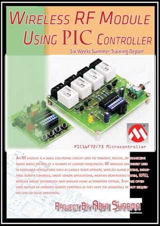
Wireless Radio Frequency Module Using PIC Microcontroller.
•
12 j'aime•10,489 vues

It's An Microcontroller Based DIY Electronics Project. Named Wireless RF Module Using PIC Microcontroller. An RF module is a small electronic circuit used to transmit, receive, or transceive radio waves on one of a number of carrier frequencies. RF modules are widely used in consumer applications such as garage door openers, wireless alarm systems, industrial remote controls, smart sensor applications, weather monitoring system, RFID, wireless mouse technology and wireless home automation systems. They are often used instead of infrared remote controls as they have the advantage of not requiring line-of-sight operation. Stay tuned for Furthur Links, Thanxx. Created By: Abhi Sharma

Recommandé
Recommandé
Contenu connexe
Tendances
Tendances (20)
En vedette
En vedette (20)
Similaire à Wireless Radio Frequency Module Using PIC Microcontroller.
Similaire à Wireless Radio Frequency Module Using PIC Microcontroller. (20)
Plus de Abee Sharma
Plus de Abee Sharma (8)
Dernier
Dernier (7)
Wireless Radio Frequency Module Using PIC Microcontroller.
- 1. Wireless RF Module Using PIC Controller Six Weeks Summer Training Report PIC16F72/73 Microcontroller An RF module is a small electronic circuit used to transmit, receive, or transceive radio waves on one of a number of carrier frequencies. RF modules are widely used in consumer applications such as garage door openers, wireless alarm systems, indus- trial remote controls, smart sensor applications, weather monitoring system, RFID, wireless mouse technology and wireless home automation systems. They are often used instead of infrared remote controls as they have the advantage of not requir- ing line-of-sight operation. Project By Abhi Sharma
- 2. ABSTRACT The Radio Frequency Module is basically a PIC Microcontroller Based Wireless Communication System. Wireless RF Module Technology enables a vast edge to any electronics project & provide many consistent advantages, which leads it to today’s up-to-date technology. An RF module is a small electronic circuit used to transmit, receive, or transceive a radio waves on one of a number of carrier frequencies. RF modules are widely used in consumer applications such as garage door openers, wireless alarm systems, industrial remote controls, smart sensor applications and wireless home automation systems. They are often used instead of infrared remote controls as they have the advantage of not requiring line-of-sight operation. Radio Frequency involves two sub units Named, Transmitter & Receiver. As their name implies transmitter is used to transmit or to send the data from input & it convert into serial port data by using HT12E encoder. This encoded data get re- ceived by receiver placing far away from it. The first job that a receiver do after receiving it, Is to convert or decode the data into parallel ports by using HT12D de- coder. After converting the data into parallel form we simply connect the receiver side circuit with relay so that we can operate AC devices (e.g. Bulb, Tube, Fan etc.) with RF Module. And, About The Matter Technology that I have used is PIC16F73. The Technology of Any Project is Considered as The Heart as well as The Mind To It. The Biggest Concern To Any Student Or Trainee Remains That The Technology He’s Going Learn Must Be Up-to-Date and Must to be In Industry’s Interest. So, That’s Why I’ve Chosen PIC Series Of Microcontrollers. They are Cost Effective, Provide Wide Availability, large user base, extensive collection of application notes, availability of low cost or free development tools, and serial programming (and re-programming with flash memory) capability. The very first thing that concern to any electronics engineering student before choosing the project is it’s Applications. That means How much innovative the proj- ect is ? And How We can make it more innovative & also make it up-to-date so that it can extend to the bigger Applications of this age of Smart & Vast life.? And, Also It’s Applications must be cost effective so that everyone can use it without any economical hesitation. There are numerous applications of wireless RF module. As, Today’s one of the vast & leading technology Named RFID is based on this principle of RF module. The wireless mouse also work on the same principle. And, beyond them Industrial Automation, Custom Wireless Remote Controls like wireless x-ray systems & Long-Range Wireless Switch System (Hand-Held), Machine To Machine (M2M) RF Wireless Networking, Robot Control , Weather Monitoring System & Identifying Objects Using RF Transmitters And Receivers and Retrieving Data Using GSM etc. could be considered as It’s Future prospects to work on. This is Indeed a great Project to work on.! ii
- 3. Acknowledgement It would be inappropriate to call this report complete and successful, If I don’t thank the people who guided as in the preparation of this project. The submis- sion of this project report gives me an opportunity to convey my gratitude to all those who have helped me to reach stage from where I have immense confidence to launch my career in the competitive world of electronics engineering. First and foremost, I would like to acknowledge my hearty thanks to the respected Mr. |------------|, HOD (ECE) for being a source of perpetual inspiration and for providing me such a nice environment for training with timely help. I would also like to express my most sincere gratitude and indebtedness to my guide Mr. |-------------| for their valuable help during the development of this project. Without his priceless suggestion and timely help I would not be able to complete this project. He has been a source of perpetual inspiration to me, towards a bright career. Not to forget the pain staking efforts of my college training and placement cell. Last but not the least I would express my utmost regards for the electronics and communication department of my Institute. ABHISHEK SHARMA B-TECH. ECE - 4TH SEM. Contact Me iii
- 4. List Of Tables & Figures Used Tables Page No. Fig: 6.6.2 Feature Table Of PIC16F73 27 Fig: 9.3 Frequencies Table Of RF 39 Figures Fig: 4.1.1 Types Of OrCAD 8 Fig: 4.3.1 A Still Of MikroC 12 Fig: 5.3.4 The Procedure Of PCB Designing Using OrCAD 16 Fig: 5.4.2 Designing a Circuit In Capture CIS 18 Fig: 5.5.3 Designing a PCB Footprint in Layout Plus 20 Fig: 6.0 Various PIC Microcontrollers Offered By Microchip 21 Fig: 6.6 Pin Diagram Of PIC16F73 24 Fig: 6.8 Flowchart Of PIC & It’s Core Architecture 28 Fig: 6.9.1 Voltage-Frequency Graph Of PIC 29 Fig: 9.3.1 RF Frequency Spectrum 40 Fig: 9.5 Block Diagram Of RF Operation 40 Fig: 9.5.1 Transmitter/Receiver Explained 41 Fig: 9.8 RF Module 45 Fig: 9.9.1 Operation Of Serial Encoder 46 Fig: 9.9.2 Operation Of Serial Decoder 47 Fig: 9.10 Flowchart Of RF Module 48 Fig: 11.1.1 RFID 51 Fig: 11.2.4 Wireless RF Based Mouse 53 Fig: 11.5 M2M PIC Tail Daughter Board 55 Fig: 11.6 Flowchart Of RF Based Control Robot 56 iv
- 5. Table Of Content Chapter No. Title Page No. Title Page i Abstract ii Acknowledgement iii List Of Tables & Figures iv 1. Introduction 1 1.1 What is Wireless.? 1 1.2 Examples Of Wireless Devices 2 1.3 Radio Frequency 2 1.4 What is RF Module ? 2 1.5 RF Module’s Performance 2 1.6 Scope of Wireless RF Module 3 2. Features Of RF Module 4 3. Hardware & Software 5 Requirements 3.1 Input Requirement 5 3.2 Output Requirement 5 3.3 Software Requirement 6 3.4 Hardware Requirement 6 4. Tools To be Used 7 4.1 OrCAD 8 4.1.1 PCB Designing 8 4.1.2 Layout Plus 9 4.1.3 Capture CIS 9 4.2 PIC Burner 10
- 6. 4.3 MikroC 11 4.4 USB PIC Bootloader 13 5. PCB Designing 14 5.1 Types Of PCB 14 5.2 Function Of PCB 14 5.3 Techniques Used 15 5.4 OrCAD Design Environment 17 5.5 Placement Of Layout Plus 19 6. Technology To be Used 21 6.1 Introduction 22 6.2 Special Microcontroller 22 Features 6.3 Peripheral Features 23 6.4 CMOS Technology 23 6.5 Data Space (RAM) 23 6.6 PIN Diagram 24 6.6.1 PIN Description 25 6.6.2 Feature Table 27 6.7 Memory Orgenization 27 6.8 Core Architecture 28 6.9 USART 29 7. Project Planning 30 7.1 Project Planning & Scheduling 30 8. Requirement Analysis 31 8.1 Listing The Components 8.1.1 Components 32 8.1.2 PCB 32 8.1.3 Capacitor 32 8.1.4 L.E.D 33 8.1.5 L.C.D 33 8.1.6 Relay 34 8.1.7 Resistor 34 8.1.8 BX433A 35 8.1.9 ULN280 1A 35 8.1.10 Battery 35 8.1.11 HT12E/ Encoder 36 8.1.12 HT12D/ Decoder 36 8.1.13 PIC16F73 37
- 7. 9. Working Of RF Module 38 9.1 Special Properties Of RF Current 38 9.2 Frequency Chart 39 9.3 RF Module Interfacing With PIC 40 9.4 Block Diagram & Explanation 40 9.5 Source Code For PIC 43 9.6 Serial Encoder/Decoder 44 9.7 Operational Working Of RF 45 9.8 Ckt Implementation 46 9.8.1 Transmitter Section 46 9.8.2 Receiver Section 47 9.9 Working Flowchart 48 10. What is Hex File Format.? 49 10.1 Structure Of Hex File Format 49 11. Applications Of RF Module 50 11.1 RFID 50 11.1.1 Operation Of RFID 50 11.1.2 Applications Of RFID 51 11.2 Wireless Mouse 52 11.2.1 RF Transmitter 52 11.2.2 RF Receiver 52 11.2.3 RF Frequency 52 11.2.4 Advantages 53 11.3 Industrial Automation 53 11.4 Custom Wireless Remote Controls 54 11.4.1 Wireless X-Ray System 54 11.4.2 Long Range Transmitter 54 11.5 Machine to Machine Wireless RF 55 Networking 11.6 Robot Using RF Remote Control 56 12. Actual PCB Photographs 57 13. Future Of Project 59 13.1 Identifying Objects 59 Using RF Technology 13.2 Radio Transmitter Design 59 13.3 Two Channels RF Control 60 13.4 Weather Monitoring System 60 14. Appendix 61 15. Bibliography 62
- 8. 1. INTRODUCTION 1.1 What is wireless ? Wireless is a term used to describe telecommunications in which electromagnetic waves (rather than some form of wire) carry the signal over part or all of the communication path. Some monitoring devices, such as intrusion alarms, employ acoustic waves at fre- quencies above the range of human hearing; these are also some- times classified as wireless. Wireless technology is rapidly evolving, and is playing an increasing role in the lives of people throughout the world. In addition, ever- larger numbers of people are relying on the technology directly or indirectly. (It has been suggested that wireless is overused in some situations, creating a social nuisance.) 1.2 Examples Of Wireless Devices • Cellular phones and pagers -- provide connectivity for portable and mobile applications, both personal and business • Global Positioning System (GPS) -- allows drivers of cars and trucks, captains of boats and ships, and pilots of aircraft to as certain their location anywhere on earth • Cordless computer peripherals -- the cordless mouse is a common example; keyboards and printers can also be linked to a computer via wireless • Cordless telephone sets -- these are limited-range devices, not to be confused with cell phones • Home-entertainment-system control boxes -- the VCR control and the TV channel control are the most common examples; some hi-fi sound systems and FM broadcast Receivers also use this technology • Remote garage-door openers -- one of the oldest wireless Devices in common use by consumers; usually operates at Radio frequencies • Two-way radios -- this includes Amateur and Citizens Radio Service, as well as business, marine, and military Communications • Baby monitors -- these devices are simplified radio transmitter/receiver units with limited range • Satellite television -- allows viewers in almost any location to select from hundreds of channels. Page 1
- 9. 1.3 Radio Frequency Radio Frequency (RF) is a rate of oscillation in the range of about 3 kHz to 300 GHz, which corresponds to the frequency of radio waves, and the alternating currents which carry radio signals. It is the use of radio signals to communicate real-time data from the warehouse floor to the WMS database and back to the floor. This expedites processing in the warehouse. Scanners collect the data and transmit it via radio frequency to antennas located throughout the warehouse. From the antennas, the signal proceeds to an access point that com- municates with the warehouse management system. This process reduces paper, data entry time delays, cycle count processing, out of stock quantities, typing errors, and misshipments. 1.4 What is RF Module? An RF Module is a (usually) small electronic circuit used to transmit, receive, or transceive radio waves on one of a number of carrier fre- quencies. RF Modules are widely used in consumer application such as garage door openers, wireless alarm systems, industrial remote controls, smart sensor applications, and wireless home automation systems. They are often used instead of infrared remote controls as they have the advantage of not requiring line-of-sight operation. 1.5 Main Factor Affecting RF Module’s Performance As with any other radio-frequency device, the performance of an RF Module will depend on a number of factors. For example, by increas- ing the transmitter power, a larger communication distance will be achieved. However, this will also result in a higher electrical power drain on the transmitter device, which will cause shorter operating life for battery powered devices. Also, using a higher transmit power will make the system more prone to interference with other RF devices, and may in fact possibly cause the device to become illegal depending on the jurisdiction. Page 2
- 10. 1.6 Typical Applications/Scope of Wireless RF Module • Vehicle Monitoring • Remote Control • Telemetry • Small-Range wireless network • Wireless meter reading • Access control systems • Wireless home security systems • Area paging • Industrial data acquisition system • Radio tags reading • RF contact less smart cards • Wireless data terminals • Wireless fire protection systems • Biological signal acquisition • Hydrological and meteorological monitoring • Robot remote control • Wireless data transmissions • Digital video/audio transmission • Digital home automation, such as remote light • Industrial remote control and remote sensing • Remote control for household appliances and Electronics projects • Mobile web server for elderly people monitoring Page 3
- 11. 2. FEATURES Of RF MoDULE There are several features of wireless RF Module: • Interference Immunity • Low Power Required • Receiver Sensitivity • RF Basics • Wireless Data Communication • Wireless Transceiver Modules • Reliable • Power Efficient • Long Range Communication • 3KHz - 300GHz of Range • Cost Effective • Small size (QLP 4x4 mm package) • True single chip UHF RF transmitter • Frequency bands: 300-348 MHz, 400-464MHz and 800-928 MHz • Programmable data rate up to 500kBaud • Low current consumption • Programmable output power up to +10dBm for all supported frequencies • Programmable baseband modulator • Ideal for multi-channel operation The RF Transmitter and Receiver modules provide • Very few external components: a simple to use RF data link at up to 300GHz from • Completely on-chip frequency any standard CMOS/TTL source. The modules are Synthesizer, very simple to operate and offers low current con- • no external filters needed sumption. Data can be supplied directly from a • Configurable packet handling hardware microprocessor or encoding device, thus keeping • Suitable for frequency hopping systems the component count down and ensuring a low due to a fast settling frequency hardware cost. These modules exhibit extremely synthesizer stable electronic characteristics due to the use of • Optional Forward Error Correction with Etched The PCB In OrCAD Technology, which uses interleaving no adjustable components and ensures very • Many powerful digital features allow a reliable operation. high-performance RF system to be made using an inexpensive microcontroller • Efficient SPI interface: All registers can be programmed with one “burst” transfer • Integrated analog temperature sensor • Support for asynchronous transparent transmit mode for backwards compatibility with existing radio communication protocols Page 4
- 12. 3. HARDWARE & SOFTWARE REQUIREMENTS 3.1 Input Requirements The Wireless RF Module has following Input Requirements: • The CPU Must Has 8-Pin Port So that The Serial Port Can Be Inserted for Burning Purposes. • If We have a Laptop Then Universal USB To Serial Port Converter Could be Used For Burning. • PIC IC is Most Important For Input The Source Code in It. • Mikro C is Also used as Input Required Software. • Any kind of sensors are also usable as input requirement. 3.2 Output Requirements For Getting the output we can use any hardware devices as follows. It all depends upon our programming requirements. As: • LCD Can be used To Receive The Output of the PIC. • LED or 7-Segments offers the Same properties as of LCD. • DC Motor or Stepper Motors or Relays are also used as output Requirement devices. • We can also use PS/2 keyboards & ADC Ports etc. Page 5
- 13. 3.3 Software Requirements • Windows , LINUX as an operating system. • OrCAD as work space for PCB designing. • TINA PRO for Simulation Purposes. • Mikro C as a Compiler for Embedded C. • PIC Burner. • Boot Loader. 3.4 Hardware Requirements • Pentium 4 Computer(Atleast). • 256 MB RAM. • Software Interfacing with PIC 16F73 Kit. • Universal USB to Serial Port Convertor Using Laptop. • 8-Pin serial port for burning the IC using CPU. • Keyboard. • Hard disk (20 GB). • Mouse. Page 6
- 14. 4. Tools Used For Development OrCAD is a proprietary software tool suite used primarily for electronic design automation. The software is used mainly by electronic design engineers and electronic technicians to create electronic schematics and electronic prints for manufacturing printed circuit boards. The name OrCAD is a portmanteau, reflecting the company and its software's origins: Oregon + CAD Page 7
- 15. 4.1 OrCAD The Cadence OrCAD product line provides affordable, high-performance PCB design tools that boost productivity for smaller design teams and individual PCB designers. 4.1.1 PCB Designing PCB stands for “PRINTED CIRCUIT BOARD”. Printed circuit board (PCB) provides both the physical structure for mounting and holding the components as well as the electrical interconnection between the components. That means a PCB or PWB (printed wiring board) is the platform upon which electronic components such as integrated circuit chips and other components are mounted. A PCB con- sists of a nonconducting substrate (typically fibre glass with epoxy as resin) upon which the conductive pattern or circuitry is formed. Copper is the most prevalent conductor although nickel, silver and tin are also used in some cases. Fig: 4.1.1 Types Of OrCAD OrCad has a long history of providing individuals and teams with a complete set of technologies that offer unprecedented productivity, seamless tool integration, and exceptional value. New 10.5 release continues that tradition. Today's lower cost and yet highly sophisticated electronic design automation systems have created a unique challenge to nearly every engineering department. Therefore the use of EDA tools has become increasingly important as product life cycles have become shorter and shorter. Modern electronic design automation (EDA) tools are beginning to support a more efficient and integrated approach to electronic. OrCad Capture® design entry is the most widely used schematic entry system in electronic design today for one simple reason: fast and universal design entry. Whether you're designing a new analog circuit, revising schematic diagram for an existing PCB, or designing a digital block diagram with an HDL module, OrCad Capture provides simple sche- matic commands you need to enter, modify and verify the design for PCB. OrCad Layout ® offers PCB designers and PCB design teams the power and flexibility to create and share PCB data and constraints across the design flow. OrCad Layout delivers all the capabilities to designers need from netlist to place and route, to final output. Page 8
- 16. 4.1.2 Layout Plus Shrinking design cycles and a growing number of nets with constraints require cus- tomers to adopt PCB design methodologies that increase predictability and acceler- ate design turnaround. Cadence® layout and routing technology offers a scalable, easy-to-use, constraint-driven PCB design solution for simple to complex PCBs, including those with RF etch components. Cadence® OrCAD® PCB Designer contains a fully integrated design flow that in- cludes a constraint manager, design capture technology, component tools, a PCB editor, an auto/interactive router, and interfaces for manufacturing and mechanical CAD. At the heart of OrCAD PCB Designer is OrCAD PCB Editor, an interactive environ- ment for creating and editing simple to complex multi-layer PCBs. The extensive feature set addresses a wide range of design and manufacturability challenges. OrCAD PCB Designer and OrCAD PCB Designer with PSpice both include Cadence SPECCTRA® for OrCAD, the market-leading PCB solution for automatic and interac- tive interconnect routing. Features Offers a proven, scalable, easy-to-use PCB editing and routing solution that grows as needed Tight, front-to-back application integration increases productivity and ensures data integrity A comprehensive feature set and a seamless PCB design environment delivers a complete solution to take a design from concept to production 4.1.3 Capture CIS OrCAD Capture provides fast and intuitive schematic design entry for PCB develop- ment or analog simulation using PSpice. The component information system (CIS) integrates with it to automatically synchronize and validate externally sourced part data. Easy-to-use and powerful, Cadence® OrCAD® Capture is the most widely used schematic design solution, supporting both flat and hierarchal designs from the simplest to the most complex. Seamless bidirectional integration with OrCAD PCB Editor enables data synchronization and cross-probing/placing between the sche- matic and the board design. OrCAD Capture allows designers to back annotate lay- out changes, make gate/pin swaps, and change component names or values from board design to schematic using the feedback process. It also comes with a large library of schematic symbols and can export net lists in a wide variety of formats. Page 9
- 17. CIS allows designers to search, identify, and populate the design with preferred parts. With easy access to company component databases and part information, designers can reduce the amount of time spent researching needed parts. Features • Boosts schematic editing efficiency of complex designs through hierarchical and Variant design capabilities. • Integrates with a robust CIS that promotes the use of preferred, current parts to Accelerate the design process and reduce project costs. • Provides access to more than two million parts with Cadence Active Parts, Offering greater flexibility when choosing design components. 4.2 PIC Burner This is the ultimate PIC/EEPROM programmer! The internet is full of PIC program- mer software. The problem is that most of the programmers support only one type of hardware and only one operating system. PIC Burner is very versatile software. We can use different kinds of hardware with it, because the pins used on parallel port can be set using a simple ini-file. We can also use different assemblers, because pburn can read all kinds of Intel hex file formats used (inhx32, inhx16 and inhx8m). Features • Linux and Windows XP/Vista/7 support • Parallel port hardware support • Program memory and configuration memory read/write/verify • Data memory read/write/verify • Reads and writes multiple hex file formats (inhx32, inhx16, inhx8m) • Input file format auto detection • Good documentation • Support for serial port hardware Page 10
- 18. 4.3 Mikro C (Compiler) 4.3.1 Introduction To MikroC MikroC is a powerful, feature rich development tool for PICmicros. It is designed to provide the programmer with the easiest possible solution for developing ap- plications for embedded systems, without compromising performance or control. PIC and C fit together well: PIC is the most popular 8-bit chip in the world, used in a wide variety of applications, and C, prized for its efficiency, is the natural choice for developing embedded systems. mikroC provides a successful match featuring highly advanced IDE, ANSI compliant compiler, broad set of hardware libraries, comprehensive documentation, and plenty of ready-to-run examples. Page 11
- 19. Fig: 4.3.1 A Still Of MikroC Features mikroC allows you to quickly develop and deploy complex applications: • Write your C source code using the built-in Code Editor (Code and Parameter Assistants, Syntax Highlighting, Auto Correct, Code Templates, and more…) • Use the included mikroC libraries to dramatically speed up the development: data Acquisition, memory, displays, conversions, communications • Monitor your program structure, variables, and functions in the Code Explorer. • Generate commented, human-readable assembly, and standard HEX compatible with all programmers. • Inspect program flow and debug executable logic with the integrated Debugger. • Get detailed reports and graphs: RAM and ROM map, code statistics, assembly Listing, calling tree, and more… • We have provided plenty of examples for you to expand, develop, and use as Building bricks in your projects. Copy them entirely if you deem fit 4.3.2 Projects mikroC organizes applications into projects, consisting of a single project file (extension .ppc) and one or more source files (extension .c). You can compile source files only if they are part of a project. The project file carries the following information: • project name and optional description, • target device, • device flags (config word), • device clock, Page 12
- 20. 4.4 USB PIC Bootloader (PIC-BOOT) A bootloader is a program that stays in the micro controller and communicates with the PC (usually through the serial interface).The bootloader receives a user program from the PC and writes it in the flash memory, then launches this program in execution. Bootloaders can only be used with those micro controllers that can write their flash memory through software as PIC16F870. USB PIC Bootloader is a resident bootloader for PIC18 series of Enhanced Flash USB Micro controllers. It allows us to program a new firmware application image into the chip using the standard USB connectivity of your device. • USB PIC Bootloader fully complies with USB Specification for Human Input Devices (HID) and all interfacing is done via standard HID driver from Microsoft. • XTEA encryption algorithm is used to protect privacy of firmware application updated With USB PIC Bootloader. • USB PIC Bootloader code is write-protected and cannot be overwritten by firmware. • Firmware update or user mode is selected by SW and/or HW switch. • USB PIC Bootloader is a small program that stays in the first 2,048 bytes of the pro Gram memory of the Microchip PIC Micro controller. • Bootloader runs at the boot time (when the processor has just been reset) and is Capable of loading a complete application program into a processor's memory. • With the USB PIC Bootloader loaded, there are two distinct modes of operation: Firmware update mode and user mode. • USB PIC Bootloader uses the EEPROM mark and/or hardware switch to determine which mode to run in. The bootloader firmware is given in the form of Basic source program that has to be compiled with PIC Simulator IDE integrated Basic compiler to get the HEX file ready to be programmed into the microcontroller. The correct micro controller model needs to be selected - 16F877(A), and the selected clock frequency is supposed to be at least 8MHz Since the start address 0000 hex is set for the boot loader software our New start is always 0010 hex. This means that when we write our code must always think that the start is at address 0010 hex. Page 13
- 21. 5. PCB Designing PCB stands for “PRINTED CIRCUIT BOARD”. Printed circuit board (PCB) provides both the physical structure for mounting and holding the components as well as the electrical interconnection between the components. That means a PCB or PWB (printed wiring board) is the platform upon which electronic components such as integrated circuit chips and other components are mounted. A PCB consists of a non-conducting substrate (typically fiber glass with epoxy as resin) upon which the conductive pattern or circuitry is formed. Copper is the most prevalent conductor although nickel, silver and tin are also used in some cases. 5.1 Types of PCB PCB may be of different types:- 1) Single-sided 2) Double-sided 3) Multilayer Single sided PCBs: - As the name suggest in these designs the conductive pattern is only at in one side. And also the size is large in these case but these are cheap. Double sided PCBs:-These are the PCBs on which the conductive pattern is in on both sides. The size of board is small in this case but it is costlier than that of above. Multilayer PCBs:- In this case the board consists of alternating layers of conducting pattern and insulating material. The conductive Material is connected across the layers through plated Through holes. The size of this PCB is smaller than that of double sided PCB but it is very costly. PCBs may also be either rigid, flexible, or the combination of two (rigid-flex). When the electronic components have been mounted on the PCB, the combination of PCB and components is an electronic assembly, also called PRINTED CIRCUIT AS- SEMBLY. This assembly is the basic building block for all the electronic appliances such as television, computer and other goods. 5.2 Function Of PCB Printed circuited boards are dielectric substrates with metallic circuitry formed on that. They are some times referred to as the base line in electronic packaging. Electronic packaging is fundamentally an inter connection technology and the PCB is the baseline building block of this technology. Page 14
- 22. 5.3 Techniques Used For PCB Designing There mainly two techniques which are use for the PCB designs. 1. Hand Taping 2. Computer Aided Design 5.3.1 PCBs using Hand Taping o PCB design using hand taping is the process of technical drawing. o In hand taping method layout should be prepared on grid paper. o In hand taping, components pads can be prepared by using black pads. o Routing of the board can be done by tapes with different widths. o Each layer (top, bottom) has to prepare separately. DISADVANTAGES OF HAND-TAPING FOR PCB DESIGNING o Each layer has to be designed separately. o We cannot generate NCD files for CNC drilling. o Difficult to modify the design in the designing process or after designing. o Difficult to get good design overview. 5.3.2 PCB Designing Using CAD All the above difficulties can be removed by using CAB system. CAD system for PCB designing requires following: o A computer system. o PCB design software like OrCad, CADSTAR, Protel, TANGO, Mentor etc. o A photo plotter for art work generation. There are many enhanced features in electronics design automation tools which not possi- ble in the hand taping. The Main Advantages Are Given Below o Auto placement o Auto routing o After routing, optimization of tracks can be done. o Provides physical design reuse modules o Electrical rule check (ERC) o All the layers are generated from the same design by giving different options. o Bill of material can be generated which contains number of different components used. o We can draw conductors as an arc, semi-circular at different angles. o Design Rule Check o Advanced CAD systems have high speed analysis. o CAD system provides all NCD files and Gerber data files for photo plotting. Page 15
- 23. 5.3.3 Basic Design System In CAD The following design steps are very common while designing a PCD in CAD: • Entry the schematic diagram. • Net list file creation. • Placement of components manually or automatically. • Routing of the board using manual routing tools or auto router • Design rule check physical and electrical. • Artwork generation. 5.3.4 Traditional Design Flow In CAD Fig: 5.3.4 The Procedure Of PCB Designing Using OrCAD 5.3.5 Designing Softwares There many softwares which are used for PCB designs. Some of them are given below:- • OrCad • CADSTAR • Protel • TANGO • Mentor The most commonly software which are used for PCB design in India are Protel and OrCad. Page 16
- 24. 5.4 OrCAD Design Environment OrCad has a long history of providing individuals and teams with a complete set of tech- nologies that offer unprecedented productivity, seamless tool integration, and exceptional value. New 10.5 release continues that tradition. Today's lower cost and yet highly sophisticated electronic design automation systems have created a unique challenge to nearly every engineering department. Therefore the use of EDA tools has become increasingly important as product life cycles have become shorter and shorter. Modern electronic design automation (EDA) tools are beginning to support a more efficient and integrated approach to electronic. OrCad Capture® design entry is the most widely used schematic entry system in electronic design today for one simple reason: fast and universal design entry. Whether you're de- signing a new analog circuit, revising schematic diagram for an existing PCB, or designing a digital block diagram with an HDL module, OrCad Capture provides simple schematic commands you need to enter, modify and verify the design for PCB. OrCad Layout ® offers PCB designers and PCB design teams the power and flexibility to create and share PCB data and constraints across the design flow. OrCad Layout delivers all the capabilities to designers need from netlist to place and route, to final output. The ease-of use and intuitive capabilities of OrCad Layout provides for quick startup and rapid learning right out of the box. 5.4.1 PCB Design Steps In OrCAD 10.5 Entry of Schematic Diagram Schematic diagram provides the functional flow and the graphical representation of an electronic circuit. The entry of schematic diagram is the first step in PCB design using OrCad. A schematic diagram consists of:- • Electrical connections(nets) • Junctions • Integrated circuits symbols • Discrete components symbols like resistors, capacitors etc. • Input / output connectors • Power and ground symbols • Buses • No connection symbols • Components reference names • Text Page 17
- 25. 5.4.2 The Schematic Page Editor The schematic page editor is used to display and edit schematic pages. So that one can parts; wires; buses and draw graphics. The schematic page editor has a tool palette that you can use to draw and place everything you need to create a schematic page. One can print from within the schematic page editor, or from the project window. Fig: 5.4.2 Designing a Circuit In Capture CIS 5.4.3 The Part Editor The part editor is used to create and edit parts. From the view menu of the part editor you can choose either part or package. In part view one can:- • Create and edit parts and symbols, then store in new or existing libraries. • Create and edit power and ground symbols, off-page connector symbols, and title block • Use the tool palette’s electrical tools to place pins on parts, and its drawing tools to draw parts and symbols. One can search for information in the session log using the find command on the Edit menu. You can also save the contents of the of the session log to a file, which is useful when working with OrCAD’s technical support to solve technical problems. The default filename is SESSION.TXT Page 18
- 26. 5.4.4 Creating Net List File Net-list file is a document file which contains information about the logical interconnec- tions between signals and pins. Before one create a net list file, be sure one’s project is completed, annotated and it is free from electrical rule violations. A net list file consists of nets, components, connectors, junctions, no connection symbol, power and ground symbols. Creation of net list in capture: • Select your design in the project manager. • From the tools, choose create net list. The net list dialog box displays. • Choose a net list format tab. • If necessary, set the part value and PCB foot print combined property strings to Reflect the information you want in the net list. • Click OK to create the net list. • In the net list file text box, enter a name for the output file. If the selected format creates an additional file, enter its file name in the second text box. 5.5 Placements Of Layout Plus: 5.5.1 What is Layout Plus ? Layout plus is one part for the PCB design in which we place as well as route the components an set unit of measurement, grids, and spacing in OrCad. Within other soft wares you also have to place and route the components in similar way. For the placement and routing of the components we normally use auto-placement and auto-routing. Unfortunately, in a lot of soft wares some critical signals have to be routed manually before auto-routing. In layout plus we also define the layer stacks, pad stacks and via's. 5.5.2 Steps for board design • At first, we have created a net list from our schematic diagram by using capture. • Layout plus includes design rules in order to guide logical placement and routing. That means, load the net list into layout to create the board. • Specify board parameters: Specifying global setting for the board, including nits of Measurements, grid, and spacing • Place components: Use the components tool in order to place manually the Components which are fixed by the system designer on the board or otherwise use Auto-placement. • Route the board: Use different routing technologies to route the board and take Advantage of push and shove (a routing technology), which moves track you are Currently routing as well as you can also auto route the board. • Provide finishing of the board: Layout supplies an ordered progression of commands on the auto menu for finishing your design. These commands include design rule check, cleanup design, rename components, back annotate, run post processor, and create reports. Page 19
- 27. 5.5.3 Method To Create a Board With Layout Plus • Ensure that net list with all footprints and necessary information has been created. • Create a directory in which the schematic design, net list, and boar will co-exit and put the schematic design and net list. OrCad provides a directory for this purpose. • From the layout session frame’s file menu, choose New. The load template file in the dialog box displayed. Fig: 5.5.3 Designing a PCB Footprint in Layout Plus 5.5.4 Placement of components: Placement of components means that to place the components in designed box. A de- signer should follow the following steps before going for it:- • Optimize the board for component placement. • Load the placement strategy file. • Place components on the board. • Optimize placement using various placements Components can be placed by using two techniques:- 1) Manual placement of components 2) Auto placement of components Choose the components tool bar button. From the pop up men, choose the queue for placement. The components selection criteria dialog box appears. Enter the reference designator of the components that you want to place in the appropriate text box, and Page 20 click ok. Drag the components to desired location, place it there.
- 28. 6. Technology To Be Used The Technology of Any Project is Considered as The Heart as well as The Mind To It. The Biggest Concern To Any Student Or Trainee Remains That The Technology He’s Gonna Learn Must Be Up-to-Date and Must to be In Industry’s Interest. So, That’s Why I’ve Choose PIC Series Of Microcontrollers. They are Cost Effective, Provide Wide Avail- ability, large user base, extensive collection of application notes, availability of low cost or free development tools, and serial programming (and re-programming with flash memory) capability. Fig: 6 Various PIC Microcontrollers Offered By Microchip The Microchip 16C84 (PIC16x84), introduced in 1993 , was the first Microchip CPU with on- chip EEPROM memory. This electrically erasable memory made it cost less than CPUs that required a quartz “Erase window” for erasing EPROM. It is generally thought that PIC stands for Peripheral Interface Controller, although General Instruments' original acronym for the initial PIC1640 and PIC1650 devices was "Programma- ble Interface Controller". The acronym was quickly replaced with "Programmable Intelligent Computer". Page 21
- 29. PIC 16 Series-PIC16F73 PIC16F73/76 devices are available only in 28-pin packages,while PIC16F74/77 devices are available in 40-pin and 44-pin packages. All devices in the PIC16F7X family share common architecture, with the following differences: • The PIC16F73 and PIC16F76 have one-half of the total on-chip memory of the PIC16F74 and PIC16F77. • The 28-pin devices have 3 I/O ports, while the 40/44-pin devices have 5. • The 28-pin devices have 11 interrupts, while the 40/44-pin devices have 12. • The 28-pin devices have 5 A/D input channels, while the 40/44-pin devices have 8. • The Parallel Slave Port is implemented only on the 40/44-pin devices. 6.1 Introduction PIC is a family of Harvard architecture microcontrollers made by Microchip Technology, derived from the PIC1640 originally developed by General Instru- ment's Microelectronics Division. The name PIC initially referred to "Peripheral Interface Controller" PICs are popular with developers and hobbyists alike due to their low cost, wide availability, large user base, extensive collection of application notes, availability of low cost or free development tools, and serial programming (and re-programming with flash memory) capability. 6.2 Special Microcontroller Features: • High performance RISC CPU. • Only 35 single word instructions to learn. • All single cycle instructions except for program branches which are two-cycle. 1. Operating speed:DC - 20 MHz clock input DC - 200ns instruction cycle. 2. Up to 8K x 14 words of FLASH Program Memory, Up to 368 x 8 bytes of Data Memory (RAM). 3. Interrupt capability (up to 12 sources). 4. Eight level deep hardware stack. 5. Direct, Indirect and Relative Addressing modes. 6. Processor read access to program memory. 7. Power-on Reset (POR). 8. Power-up Timer (PWRT) and Oscillator Start-up Timer (OST). 9. Watchdog Timer (WDT) with its own on-chip RC oscillator for reliable operation. 10. Programmable code protection. 11. Power saving SLEEP mode. 12. Selectable oscillator options. Page 22 13. In-Circuit Serial Programming(ICSP) via two pins.
- 30. 6.3 Peripheral Features: a. Timer0: 8-bit timer/counter with 8-bit prescaler. b. Timer1: 16-bit timer/counter with prescaler, can be incremented during SLEEP via external crystal/clock. c. Timer2: 8-bit timer/counter with 8-bit period register, prescaler and post Scaler. d. Two Capture, Compare, PWM modules: i. Capture is 16-bit, max. Resolution is 12.5 ns ii. Compare is 16-bit, max. Resolution is 200 ns iii. PWM max. resolution is 10-bit. e. 8-bit, up to 8-channel Analog-to-Digital converter. f. Synchronous Serial Port (SSP) with SPI (Master mode) and I2C(Slave). g. Universal Synchronous Asynchronous Receiver Transmitter (USART/SCI). h. Parallel Slave Port (PSP), 8-bits wide with external RD, WR and CS controls (40/44-pin only). i. Brown-out detection circuitry for Brown-out Reset (BOR). 6.4 CMOS Technology: a. Low power, high speed CMOS FLASH technology. b. Fully static design. c. Wide operating voltage range: 2.0V to 5.5V. d. High Sink/Source Current: 25 mA. e. Industrial temperature range. f. Low power consumption: i. < 2 mA typical @ 5V, 4 MHz 6.5 Data space (RAM) PICs have a set of registers that function as general purpose RAM. Special pur- pose control registers for on-chip hardware resources are also mapped into the data space. The addressability of memory varies depending on device series, and all PIC devices have some banking mechanism to extend addressing to additional memory. Later series of devices feature move instructions which can cover the whole addressable space, independent of the selected bank. In earlier devices, any register move had to be achieved via the accumulator. To implement indirect addressing, a "file select register" (FSR) and "indirect reg- ister" (INDF) are used. A register number is written to the FSR, after which reads from or writes to INDF will actually be to or from the register pointed to by FSR. Later devices extended this concept with post- and pre- increment/decrement for greater efficiency in accessing sequentially stored data. This also allows FSR to be treated almost like a stack pointer (SP). Page 23
- 31. 6.6 Pin Diagram Fig: 6.6 Pin Diagram Of PIC16F73 Page 24
- 32. 6.6.1 Pin Description (••) MCLR-(pin 1) PIC16F7X devices have a noise filter in the MCLR Reset path. The filter will detect and ignore small pulses. It should be noted that a WDT Reset does not drive MCLR pin low. The behaviour of the ESD protection on the MCLR pin has been altered from previous devices of this family. Voltages applied to the pin that exceed its specification can result in both MCLR Resets and excessive current beyond the device specification during the ESD event. For this reason, Microchip recommends that the MCLR pin no longer be tied directly to VDD. (••) RESET The PIC16F7X differentiates between various kinds of RESET: • Power-on Reset (POR) • MCLR Reset during normal operation • MCLR Reset during SLEEP • WDT Reset (during normal operation) • WDT Wake-up (during SLEEP) • Brown-out Reset (BOR) Some registers are not affected in any RESET condion. Their status is unknown on POR and unchanged n any other RESET. Most other registers are reset to a RESET state” on Power-on Reset (POR), on the MCLR and WDT Reset, on MCLR Reset during LEEP, and Brown-out Reset (BOR). They are not affected by a WDT Wake-up, which is viewed as the resumption of normal operation. The TO and PD bits are set or cleared differently in different RESET situations, as indicated (••) PORTA –(pin 2 to 7)and the TRISA Register PORTA is a 6-bit wide, bi-directional port. The corresponding data direction register is TRISA. Setting a TRISA bit (= ‘1’) will make the corresponding PORTA pin an input (i.e., Put the corresponding output driver in a Hi-Impedance mode). Clearing a TRISA bit (= ‘0’) will make the corresponding PORTA pin an output (i.e., put the contents of the output latch on the selected pin). Reading the PORTA register reads the status of the pins, whereas writing to it will write to the port latch. All write operations are read-modify-write opera- tions. Therefore, a write to a port implies that the port pins are read, the value is modified and then written to the port data latch. (••) GND –(pin 8) Provide Ground to it. (••) OSC1/CLK IN -(pin 9) Page 25 Oscillator crystal input/external clock source input.
- 33. (••) OSC2/CLK OUT-(pin 10) Oscillator crystal output. Connects to crystal or resonator in Crystal Oscillator mode. In RC mode, the OSC2 pin outputs CLK OUT which has 1/4 the frequency of OSC1, and denotes the instruction cycle rate. Oscillator Type: The PIC16F7X can be operated in four different oscillator modes: • LP Low Power Crystal • XT Crystal/Resonator • HS High Speed Crystal/Resonator • RC Resistor/Capacitor (••) PORTC and the TRISC Register(pin 11 to 18) PORTC is an 8-bit wide, bi-directional port. The corresponding data direction register is TRISC. Setting a TRISC bit (= ‘1’) will make the corresponding PORTC pin an input (i.e., put the corresponding output driver in a Hi-Impedance mode). Clearing a TRISC bit (= ‘0’) will make the corresponding PORTC pin an output (i.e., put the contents of the output latch on the selected pin). PORTC is multiplexed with several peripheral functions PORTC pins have Schmitt Trig- ger input buffers. When enabling peripheral functions, care should be taken in defin- ing TRIS bits for each PORTC pin. (••) Vss(pin 19) Ground reference for logic and I/O pins (••) Vdd(pin 20) Positive supply for logic and I/O pins (••) PORTB and The TRISB Register(pin 21 to 28) PORTB is an 8-bit wide, bi-directional port. The corresponding data direction register is TRISB. Setting a TRISB bit (= ‘1’) will make the corresponding PORTB pin an input (i.e., put the corresponding output driver in a Hi-Impedance mode). Clearing a TRISB bit (= ‘0’) will make the corresponding PORTB pin an output (i.e., Put the contents of the output latch on the selected pin). Each of the PORTB pins has a weak internal pull-up. A single control bit can turn on all the pull-ups. The weak pull-up is automatically turned off when the port pin is configured as an output. The pull-ups are disabled on a Power-on Reset. Page 26
- 34. 6.6.2 Feature Table Of PIC16F73 Fig: 6.6.2 Feature Table Of PIC16F73 6.7 Memory Organization There are two memory blocks in each of these PICmicro® MCUs. The Program Memory and Data Memory have separate buses so that concurrent access can Occur and is detailed in this section. The Program Memory can be read internally By user code. Additional information on device memory may be found in the PICmicro Mid- Page 27 Range Reference Manual.
- 35. 6.8 Core Architecture Fig: 6.8 Flowchart Showing a typical microcontroller device and its different sub-Units The PIC architecture is distinctively minimalist. It is characterized by the follow- ing features: • Separate code and data spaces (Harvard architecture) • A small number of fixed length instructions • Most instructions are single cycle execution (4 clock cycles), with single delay cycles upon branches and skips • A single accumulator (W), the use of which (as source operand) is implied (i.e. is not encoded in the opcode) • All RAM locations function as registers as both source and/or destination of math and other functions. • A hardware stack for storing return addresses • A fairly small amount of addressable data space (typically 256 bytes), Extended through banking • Data space mapped CPU, port, and peripheral registers • The program counter is also mapped into the data space and writable (this is used to implement indirect jumps). Unlike most other CPUs, there is no distinction between memory space and reg- ister space because the RAM serves the job of both memory and registers, and Page 28 the RAM is usually just referred to as the register file or simply as the registers.
- 36. Advantages The PIC architectures have these advantages: • Small instruction set to learn. • RISC architecture. • Built in oscillator with selectable speeds. • Easy entry level, in circuit programming plus in circuit debugging. • PICKit units available from Microchip.com for less than $50. • Inexpensive microcontrollers. • Wide range of interfaces including I²C, SPI, USB, USART, A/D, programmable comparators, PWM, LIN, CAN, PSP, and Ethernet. 6.9 Universal Synchronous Asynchronous Receiver &Transmitter(USART) The Universal Synchronous Asynchronous Receiver Transmitter (USART) module is one of the two serial I/O modules. (USART is also known as a Serial Communications Interface or SCI.) The USART can be configured as a full duplex asynchronous system that can communicate with pe- ripheral devices, such as CRT terminals and personal computers, or it can be configured as a half duplex synchronous system that can commu- nicate with peripheral devices, such as A/D or D/A integrated circuits, serial EEPROMs, etc. The USART can be configured in the following modes • Asynchronous (full duplex) • Synchronous - Master (half duplex) • Synchronous - Slave (half duplex) Bit SPEN (RCSTA<7>) and bits TRISC<7:6> have to be set in order to config- ure pins RC6/TX/CK and RC7/RX/DT as the Universal Synchronous Asyn- chronous Receiver Transmitter. 6.9.1 PIC16F73 Voltage-Frequency Graph Page 29 Fig: 6.9.1 The V-F Graph Of PIC
- 37. 7. Project Planning 7.1 Project Planning & Scheduling The planning stage establishes a bird’s eye view of the intended software product, and uses this to establish the basic project structure, evaluate feasibility and risks associated with the project, and describe appropriate management and technical approaches. Project planning is part of Project Management. It is a well-established approach to managing and controlling the introduction of new initiatives or organisational changes. Projects are finite in length, usually one-time pieces of work involving a number of activities that must be completed within a given time frame, and often on a fixed budget. While the very simplest projects can be managed easily by applying common sense and just getting on with things, projects that are more complex need a great deal of planning, and benefit from a formal, disciplined management approach. From making sure that activities will actually meet the specified need, to devising a workable schedule, developing systems for reporting progress, and managing re- quests for changes – all of these issues require thoughtful consideration. Managing projects well requires a great deal of time, skill, and finesse. There are many sides to project management and this is what makes it so interesting and demanding. 7.1.1 Project Planning Includes • Dividing the project into plannable stages • When to build the project plan • Who constructs the project plan • Step by step guide to constructing a project plan • Making the project plan visible, getting the project plan used • Independent project plan reviews • Getting resource commitments • Time recording • Tracking progress against the project plan • Revising the project plan during the project Now, After The Project Planning I’m Very Interested to Add The List Of The Components That’s been Used in the Wireless RF Module Project. So, Here’s Gonna Be The Step By Step Listing Of Components Of This Project Under Requirement Analysis. Page 30
- 38. 8. REQUIREMENT ANALYSIS Requirement Analysis in electronics engineering, encompasses those tasks that go into determining the needs or conditions to meet for a new or altered prod- uct, taking account of the possibly conflicting requirements of the various stake- holders, such as beneficiaries or users. Requirement analysis is critical to the success of a development project. Require- ments must be documented, actionable, measurable, testable, related to identi- fied business needs or opportunities, and defined to a level of detail sufficient for system design. Requirements can be functional and non-functional. Any coherent and reasonable system must have requirements that define what the system is ultimately supposed to do. A requirement is an objective that must be met. Planners cast most requirements in functional terms, leaving design and implementation details to the developers. In this wireless RF Module Project, we implemented this phase of requirements gathering by collecting information from various sources like internet & also by eternal knowledge of our trainees. The requirement of any electronics project must be it’s components & the circuit diagram created by using OrCAD & an etched PCB. Conceptually, requirements analysis includes the components used while created this project. Well, the Softwares & a PC with some other stuff(like soldering wire etc.) also come under requirement section but they’ve been already pasted in ‘Tools To Be Used’ section, So here’s goes the Components list section, named “Listing The Components”.!! Page 31
- 39. 8.1 Listing The Components 8.1.1 Component Component is Defined As: An Artifact That is One of The Individual Parts of Which a Composite Entity is Made Up; Especially a Part That Can be Separated From or Attached To a System. So, With The Help Of This Defination We Can Guess The Importance Of Components In Elec- tronics Projects. Components Are The Working Modules Of Any Project That Makes It a Worth To Work. Here, In This Sub Chapter I’m Going To Write The List Of Compo- nents That’s Been Used To Make This Project a Worth Device. 8.1.2 Printed Circuit Board A printed circuit board, or PCB, is used to mechanically support and electrically con- nect electronic components using conductive pathways, tracks or signal traces etched from copper sheets laminated onto a non-conduc- tive substrate. It is also referred to as printed wiring board (PWB) or etched wiring board. Printed circuit boards are used in virtually all but the simplest commercially produced electronic devices. A PCB populated with electronic components is called a printed circuit assembly (PCA), printed circuit board assembly or PCB Assem- bly (PCBA). In informal use the term “PCB” is used both for bare and assembled boards, the context clarifying the meaning. 8.1.3 Capacitor A capacitor (originally known as condenser) is a passive two-terminal electrical compo- nent used to store energy in an electric field. The forms of practical capacitors vary widely, but all contain at least two electrical conduc- tors separated by a dielectric (insulator); for example, one common construction consists of metal foils separated by a thin layer of insulating film. Capacitors are widely used as parts of electrical circuits in many common electrical devices. Page 32
- 40. 8.1.4 Light-Emitting Diode A light-emitting diode (LED) is a semiconductor light source. LEDs are used as indicator lamps in many devices and are increasingly used for other lighting. Introduced as a practical electronic component in 1962, early LEDs emitted low-intensity red light, but modern versions are available across the visible, ultraviolet, and infrared wavelengths, with very high brightness. When a light-emitting diode is forward-biased (switched on), electrons are able to recombine with electron holes within the device, releasing energy in the form of photons. This effect is called electroluminescent and the colour of the light (corresponding to the energy of the photon) is determined by the energy gap of the semiconductor. LEDs are often small in area (less than 1 mm2), and integrated optical components may be used to shape its radiation pattern. LEDs present many advan- tages over incandescent light sources including lower en- ergy consumption, longer lifetime, improved robustness, smaller size, and faster switching. LEDs powerful enough for room lighting are relatively expensive and require more precise current and heat management than com- pact fluorescent lamp sources of comparable output. 8.1.5 Liquid Crystal Display Liquid crystal display (LCD) is a flat panel display, electronic visual display, or video display that uses the light modulat- ing properties of liquid crystals (LCs). LCs do not emit light directly. LCD displays are available to display arbitrary images (as in a general-purpose computer display) or fixed images which can be displayed or hidden, such as preset words, digits, 7-segment displays, etc., as in a digital clock. They use the same basic technology, except that arbitrary images are made up of a large number of small pixels, while other displays have larger elements. The LCD is more energy efficient and offers safer disposal than a CRT. Its low electrical power consumption enables it to be used in battery-powered electronic equipment. It is an electronically modulated optical device made up of any number of segments filled with liquid crystals and arrayed in front of a light source (backlight) or reflector to produce images in colour or monochrome. Liquid crystals were first developed in 1888. Page 33
- 41. 8.1.6 Relay A Relay is an electrically operated switch. Many relays use an electromagnet to operate a switching mecha- nism mechanically, but other operating principles are also used. Relays are used where it is necessary to control a circuit by a low-power signal (with complete electrical isolation between control and controlled circuits), or where several circuits must be controlled by one signal. A type of relay that can handle the high power required to directly control an electric motor or other loads is called a contactor. Solid-state relays control power cir- cuits with no moving parts, instead using a semiconduc- tor device to perform switching. Relays with calibrated operating characteristics and sometimes multiple op- erating coils are used to protect electrical circuits from overload or faults; in modern electric power systems these functions are performed by digital instruments still called “protective relays”. 8.1.7 Resistors A resistor is a passive two-terminal electrical component that implements electrical resistance as a circuit element. The current through a resistor is in direct proportion to the voltage across the resistor's terminals. Thus, the ratio of the voltage applied across a resistor's terminals to the intensity of current through the circuit is called resist- ance. Practical resistors have a series inductance and a small parallel capacitance; these specifications can be important in high-frequency applications. In a low-noise amplifier or pre-amp, the noise characteristics of a resistor may be an issue. The unwanted inductance, excess noise, and temperature coefficient are mainly dependent on the technology used in manufacturing the resistor. A family of discrete resistors is also characterized according to its form factor, that is, the size of the device and the position of its leads (or terminals) which is relevant in the practical manufacturing of circuits using them. Page 34
- 42. 8.1.8 BX R433A The BX R433A/433.92/TO39-1.5 is a true one-port, surface-acoustic-wave (SAW) resonator in a low-profile metal TO-39 case. It provides reliable, funda- mental-mode, quartz frequency Stabilization i.e. in transmitters or local oscillators operat- ing at 433.920 MHz. SAW - Surface Acoustic Wave Resonators are being rec- ognized by more and more public figures because of its good features and performances. They have been widely used in communication, CATV, wireless remote control, satellite receivers, radio and video transmission fields. VTC can supply you high performance, high quality and stability SAW resonators which frequencies cover from 50MHz to 1GHz. 8.1.9 ULN2801A The ULN2801A is a high-voltage, high-current Darlington transistor array. The device consists of eight npn Darlington pairs that feature high-voltage outputs with common-cathode clamp diodes for switching inductive loads. The collector-current rating of each Darlington pair is 500 mA and Output Voltage is upto 50V. The Darlington pairs may be connected in parallel for higher current Capability. Applications include relay drivers, hammer drivers, lamp drivers, display drivers (LED and gas discharge), line drivers, and logic buffers. The ULN2801A has a 2.7-kΩ series base resistor for each Darlington pair for operation directly with TTL or 5-V CMOS devices. 8.1.10 Battery An electrical battery is one or more electrochemical cells that convert stored chemical energy into electrical en- ergy. There are two types of batteries: primary batteries (dis- posable batteries), which are designed to be used once and discarded, and secondary batteries (rechargeable batteries), which are designed to be recharged and used multiple times. Page 35
- 43. 8.1.11 HT12E/212 Series of Encoder The 212 encoders are a series of CMOS LSIs for remote control system applications. They are capable of en- coding information which consists of N address bits and 12N data bits. Each address/ data input can be set to one of the two logic states. The programmed ad- dresses/data are transmitted together with the header bits via an RF or an infrared transmission medium upon receipt of a trigger signal. The capability to select a TE trigger on the HT12E or a DATA trigger on the HT12A further enhances the application flexibility of the 212 series of encoders. The HT12A additionally provides a 38kHz carrier for infrared systems. Features • Operating voltage -2.4V~5V for the HT12A -2.4V~12V for the HT12E • Low power and high noise immunity CMOS technology • Low standby current: 0.1 (type.) at VDD=5V A • HT12A with a 38kHz carrier for infrared transmission medium • Minimum transmission word -Four words for the HT12E -One word for the HT12A • Built-in oscillator needs only 5% resistor • Data code has positive polarity • Minimal external components • HT12A/E: 18-pin DIP/20-pin SOP package 8.1.12 HT12D/212 Series of Decoders The 212 decoders are a series of CMOS LSIs for remote control system applications. They are paired with Holtek’s 212 series of encoders (refer to the encoder/decod- er cross reference table). For proper operation, a pair of encoder/decoder with the same number of address- es and data format should be chosen. The decoders receive serial addresses and data from a programmed 212 series of encoders that are transmitted by a carrier using an RF or an IR transmission medium. They compare the serial input data three times continuously with their local addresses. If no error or unmatched codes are found, the input data codes are decoded and then transferred to the output pins. The VT pin also goes high to indicate a valid transmission. The 212 series of decoders are capable of decoding informations that consist of N bits of address and 12N bits of data. Of this series, the HT12D is arranged to provide 8 address bits and 4 data bits, and HT12F is used to decode 12 bits of address information. Page 36
- 44. Features • Operating voltage: 2.4V~12V • Low power and high noise immunity CMOS Technology • Low standby current • Capable of decoding 12 bits of information • Binary address setting • Received codes are checked 3 times • Address/Data number combination -HT12D: 8 address bits and 4 data bits -HT12F: 12 address bits only • Built-in oscillator needs only 5% resistor • Valid transmission indicator • Easy interface with RF or an infrared transmission Medium • Minimal external components • Pair with Holtek’s 212 series of encoders • 18-pin DIP, 20-pin SOP package 8.1.13 PIC16F73 PIC is a powerful (200 nanosecond instruction execu- tion) yet easy-to-program (only 35 single word instruc- tions) CMOS FLASH-based 8-bit microcontroller packs Microchip’s powerful PIC® architecture into 28-pin pack- age and is upwards compatible with the PIC16C5X, PIC- 12CXXX and PIC16C7X devices. The PIC16F73 features 5 channels of 8-bit Analog-to-Digital (A/D) converter with 2 additional timers, 2 capture/compare/PWM func- tions and the synchronous serial port can be configured as either 3-wire Serial Peripheral Interface (SPI) or the 2-wire Inter-Integrated Circuit (IC) bus and a Universal Asynchronous Receiver Transmitter (USART). All of these features make it ideal for more advanced level A/D applications in automotive, industrial, appliances and consumer applications. Features Parameter Name Value Program Memory Type Flash Program Memory (KB) 7 CPU Speed (MIPS) 5 • 2 PWM 10-bit RAM Bytes Digital Communication 192 • 25mA sink/source per I/O Peripherals 1-A/E/USART, 1-SSP(SPI/I2C) • 2 Capture/Compare Capture/Compare/ PWM Peripherals 2 CCP • Parallel Slave Port Timers 2 x 8-bit, 1 x 16-bit ADC 5 ch, 8-bit Temperature Range (C) -40 to 125 Operating Voltage Range (V) 2 to 5.5 Page 37 Pin Count 28
- 45. 9. Working Of RF Module As In The Very First Chapter Of This Report The Introduction has been Pasted. But Now In This Chapter I’m Going To Tell The Operating Functionality Of Wireless Radio Frequency Module Using PIC 16F73. Before Just Directing to the working of RF Module Let us read abut the RF Current It’s Behaviour first. 9.1 Special Properties Of RF Current Electric currents that oscillate at radio frequencies have special properties not shared by direct current or alternating current of lower frequencies. The en- ergy in an RF current can radiate off a conductor into space as electromagnetic waves (radio waves); this is the basis of radio technology. RF current does not penetrate deeply into electrical conductors but flows along their surfaces; this is known as the skin effect. For this reason, when the human body comes in con- tact with high power RF currents it can cause superficial but serious burns called RF burns. RF current can easily ionize air, creating a conductive path through it. This property is exploited by high frequency units used in electric arc welding, which use currents at higher frequencies than power distribution uses. Another property is the ability to appear to flow through paths that contain insulating material, like the dielectric insulator of a capacitor. When conducted by an ordi- nary electric cable, RF current has a tendency to reflect from discontinuities in the cable such as connectors and travel back down the cable toward the source, causing a condition called standing waves, so RF current must be carried by spe- cialized types of cable called transmission line. 9.2 Main Factors Affecting RF Module’s Performance As with any other radio-frequency device, the performance of an RF Module will depend on a number of factors. For example, by increasing the transmit- ter power, a larger communication distance will be achieved. However, this will also result in a higher electrical power drain on the transmitter device, which will cause shorter operating life for battery powered devices. Also, using a higher transmit power will make the system more prone to interference with other RF devices, and may in fact possibly cause the device to become illegal depending on the jurisdiction. Correspondingly, increasing the receiver sensitivity will also increase the effec- tive communication range, but will also potentially cause malfunction due to interference with other RF devices. Page 38
- 46. 9.3 Frequencies Chart Fig: 9.3 Frequencies Table Of RF Page 39
- 47. Fig 9.3.1: RF Frequency Spectrum 9.4 RF Module Interfacing with PIC The term wireless is very much hyped! Whenever we hear the term wireless, stuffs like Mobile telecommunication (GSM), Wi-Fi,Bluetooth, RF Communication,Wireless net- works, Zigbee, I2C, SPI,DTMF, 802.11b, SimpliciTI etc etc etc. Well, fortunately or unfor- tunately, all of these protocols can be interfaced with a microcontroller in one way or the other. But what matters is, The level of complexity. To start off, RF (Radio Frequency) Communication is the most preferred and low cost solution. All we need is a RF Module (Transmitter-Receiver Pair). Now, that’s not all. RF Communication works on the principle of Serial Communication. Thus, We need some- thing which converts the conventional n-bit (4-bit, 8-bit, 16-bit, etc) data into serial data. For this, we have two choices: • Use a microcontroller to convert the n-bit data into serial data and vice- versa • Use serial encoders/decoders to do the same. But, If We Use the Both Then It Would Be More Innovative Impressive As We’ll Be Able To Get The Output On L.C.D As Well. For L.C.D Interfacing With Encoder/Decode Serial Ports We Strongly Need a Microcontroller, Which In Our Project is PIC 16F73. So Here’s The Working Below: 9.5 RF Communication Block Diagram Fig: 9.5 Block Diagram Of RF Operation Page 40
- 48. A general RF communication block diagram is shown above. Since most of the encod- ers/decoders/microcontrollers are TTL compatible, most of the inputs by the user will be given in TTL logic level. Thus, this TTL input is to be converted into serial data input using an encoder or a microcontroller. This serial data can be directly read using the RF Transmitter, which then performs ASK (in some cases FSK) modulation on it and trans- mit the data through the antenna. In the receiver side, the RF Receiver receives the modulated signal through the antenna, performs all kinds of processing, filtering, demodulation, etc and gives out a serial data. This serial data is then converted to a TTL level logic data, which is the same data that the user has input. RF Modules are used wireless transfer data. This makes them most suitable for remote control applications, as in where we need to control some machines or robots without getting in touch with them (may be due to various reasons like safety, etc). Now de- pending upon the type of application, the RF module is chosen. For short range wireless control applications, an ASK RF Transmitter-Receiver Module of frequency 315 MHz or 433 MHz is most suitable. Fig: 9.5.1 Transmitter/Receiver Explained Page 41
- 49. Features • Range in open space(Standard Conditions) : 100 Meters • RX Receiver Frequency : 433 MHz • RX Typical Sensitivity : 105 Dbm • RX Supply Current : 3.5 mA • RX IF Frequency : 1MHz • Low Power Consumption • Easy For Application • RX Operating Voltage : 5V • TX Frequency Range : 433.92 MHz • TX Supply Voltage : 3V ~ 6V • TX Out Put Power : 4 ~ 12 Dbm This has single channel for data transfer, thus serial data communication is used. Antenna Now that all the connections are made, we must choose an antenna for signal trans- mission. Usually, a 20-30 cm wire serves best. It is sufficient to give a range of 80 meters in open region. To improve the efficiency, we can also use a coiled wire (take a wire and make it into a coil). It increases the signal strength. Page 42
- 50. 9.6 Source Code For PIC Since, As We Know The PIC 16F73 is a Micro-Controller Which Without a Pogramming Code is As Dumb As a Small Plastic Stuff With Having Some Sharp Pins. So, To Make This PIC Our Project’s CPU We’ve Added The Following Programming Written In Embedded C Using MikroC As a Compiler. Void main() { TRISC=0X0f; PORTB=0; // PORTC is Considered As Input PORTB As Output. LCD_Init(PORTB); // Initilize The LCD Connected On PORTB. LCD_Cmd(LCD_CLEAR); // Clear display. LCD_Cmd(LCD_CURSOR_OFF); // Turn cursor off. LCD_Out(1,1,Device 1 is ); LCD_Out(2,1,Device 2 is ); LCD_Out(2,9,OFF); LCD_Out(1,9,OFF); while(1) // An Infinite Loop. { if(PORTC.F0==0) { LCD_Out(2,9,OFF); LCD_Out(1,9,OFF); PORTC.F6=0; // The Decision Oriented Pin Of PORTC. PORTC.F7=0; // The Decision Oriented Pin Of PORTC. } if(PORTC.F1==0) { LCD_Out(2,9,OFF); LCD_Out(1,9,ON); PORTC.F6=1; PORTC.F7=0; } if(PORTC.F2==0) { LCD_Out(2,9,ON); LCD_Out(1,9,OFF); PORTC.F6=0; PORTC.F7=1; } if(PORTC.F3==0) { LCD_Out(2,9,ON); LCD_Out(1,9,ON); PORTC.F6=1; PORTC.F7=1; } }} Page 43