SlideShare une entreprise Scribd logo
1  sur  7
Télécharger pour lire hors ligne
International Journal of Engineering Inventions
e-ISSN: 2278-7461, p-ISSN: 2319-6491
Volume 3, Issue 11 (June 2014) PP: 1-7
www.ijeijournal.com Page | 1
Design of Low Voltage and High Speed Double-Tail Dynamic
Comparator for Low Power Applications
K. Sumalatha1
, Mr. B. Prathap reddy2
1, 2
(P.G. Student, Assistant Professor, Department of ECE, Santhiram Engineering College Nandyal)
Abstract: Comparators are basic building elements for designing modern analog and mixed signal systems.
Speed and resolution are two important factors which are required for high speed applications. This paper
presents a design for an on chip high-speed dynamic latched comparator for high frequency signal digitization.
The dynamic latched comparator consists of two cross coupled inverters comprising a total of 9 MOS
transistors. The measured and simulation results show that the dynamic latched comparator design has higher
speed, low power dissipation and occupying less active area compared to double tail latched and preamplifier
based clocked comparators. A new fully dynamic latched comparator which shows lower offset voltage and
higher load drivability than the conventional dynamic latched comparators has been designed. With two
additional inverters inserted between the input-stage and output-stage of the conventional double-tail dynamic
comparator, the gain preceding the regenerative latch stage was improved and the complementary version of
the output-latch stage, which has bigger output drive current capability at the same area, was implemented.
Keywords: Comparator, Double-Tail Comparator.
I. Introduction
Due to fast speed, low power consumption, high input impedance and full-swing output, dynamic
latched comparators are very attractive for many applications such as high-speed analog-to digital converters
(ADCs), Memory sense amplifiers (SAs) and data receivers. They use positive feedback mechanism with one
pair of back to-back cross coupled inverters (latch) in order to convert a small input-voltage difference to a full-
scale digital level in a short time. However, an input-referred latch offset voltage, resulting from static
mismatches such as threshold Permission to make digital or hard copies of all or part of this work for personal
or classroom use is granted without fee provided that copies are not made or distributed for profit or commercial
advantage and that copies bear this notice and the full citation on the first page. To copy otherwise, or republish,
to post on servers or to redistribute to lists, requires prior specific permission and/or a fee
Fig 1 High speed voltage comparator
In this paper, we present a new dynamic latched comparator which shows lower input-referred latch
offset voltage and higher load drivability than the conventional dynamic latched comparators. With two
additional inverters inserted between the input- and output-stage of the conventional double-tail dynamic
comparator, the gain preceding the regenerative latch stage was improved and the complementary version of the
output-latch stage, which has bigger output drive current capability at the same area, was implemented. As a
result, the circuit shows up to 25% less input referred latch offset voltage and 44% less sensitivity of the delay
versus the input voltage difference (delay/log(!Vin)), which is about 17.4ps/decade, than the conventional
double-tail latched comparator at approximately the same area and power consumption.
Design Of Low Voltage And High Speed Double-Tail Dynamic Comparator For Low Power
www.ijeijournal.com Page | 2
II. Clockedregenerative Comparators
Clocked regenerative comparators have found wide applications in many high-speed ADCs since they
can make fast decisions due to the strong positive feedback in the regenerative latch. Recently, many
comprehensive analyses have been presented, which investigate the performance of these comparators from
different aspects, such as noise [11], offset [12], [13], and [14], random decision errors [15], and kick-back noise
[16]. In this section, a comprehensive delay analysis is presented; the delay time of two common structures, i.e.,
conventional dynamic comparator and conventional dynamic double-tail comparator are analyzed, based on
which the proposed comparator will be presented.
A. Conventional Dynamic Comparator
The schematic diagram of the conventional dynamic comparator widely used in A/D converters, with high input
impedance, rail-to-rail output swing, and no static power consumption is shown in Fig. 1 [1], [17]. The
operation of the comparator is as follows. During the reset phase when CLK = 0 and Mtail is off, reset
transistors (M7–M8) pull both output nodes Outn and Outp to VDD to define a start condition and to have a
valid logical level during reset. In the comparison phase, when CLK = VDD, transistors M7 and M8 are off, and
Mtail is on. Output voltages (Outp, Outn), which had been pre-charged to VDD, start to discharge with different
discharging rates depending on the corresponding input voltage (INN/INP). Assuming the case where VINP >
VINN, Outp discharges faster than Outn, hence when Outp (discharged by transistor M2 drain current), falls
down to VDD–|Vthp| before Outn (discharged by transistor M1 drain current), the corresponding pMOS
transistor (M5) will turn on initiating the latch regeneration caused by back-to-back inverters (M3, M5 and M4,
M6). Thus, Outn pulls to VDD and Outp discharges to ground. If VINP < VINN, the circuits works viceversa.
Fig2:Conventional Dynamic Comparator
As shown in Fig. 2, the delay of this comparator is comprised of two time delays, t0 and tlatch. The
delay t0 represents the capacitive discharge of the load capacitance CL until the first p-channel transistor
(M5/M6) turns on. In case, the voltage at node INP is bigger than INN (i.e., VINP > VINN), the drain current of
transistor M2 (I2) causes faster discharge of Outp node compared to the Outn node, which is driven by M1 with
smaller current. Consequently, the discharge delay (t0) is given by
In (1), since I2 = Itail/2 + _Iin = Itail/2 + gm1,2_Vin, for small differential input (_Vin), I2 can be approximated
to be constant and equal to the half of the tail current. The second term, tlatch, is the latching delay of two
crosscoupled inverters. It is assumed that a voltage swing of _Vout = VDD/2 has to be obtained from an initial
output voltage difference _V0 at the falling output (e.g., Outp). Half of the supply voltage is considered to be the
threshold voltage of the comparator following inverter or SR latch [17]. Hence, the latch delay time is given by,
[18]
Design Of Low Voltage And High Speed Double-Tail Dynamic Comparator For Low Power
www.ijeijournal.com Page | 3
where gm,eff is the effective transconductance of the back-toback inverters. In fact, this delay depends, in a
logarithmic manner, on the initial output voltage difference at the beginning of the regeneration (i.e., at t = t0).
Based on (1), _V0 can be calculated from (3)
The current difference, _Iin = |I1 − I2|, between the
branches is much smaller than I1 and I2. Thus, I1 can be approximated by Itail/2 and (3) can be rewritten as
In this equation, β1,2 is the input transistors’ current factor and Itail is a function of input common-mode
voltage (Vcm) and VDD. Now, substituting _V0 in latch delay expression and considering t0, the expression for
the delay of the conventional dynamic comparator is obtained as
Equation (5) explains the impact of various parameters. The total delay is directly proportional to the
comparator load capacitance CL and inversely proportional to the input difference voltage (_Vin). Besides, the
delay depends indirectly to the input common-mode voltage (Vcm). By reducing Vcm, the delay t0 of the first
sensing phase increases because lower Vcm causes smaller bias current (Itail). On the other hand, (4) shows that
a delayed discharge with smaller Itail results in an increased initial voltage difference (_V0), reducing tlatch.
Simulation results show that the effect of reducing the Vcm on increasing of t0 and reducing of tlatch will finally
lead to an increase in the total delay. In [17], it has been shown that an input common-mode voltage of 70% of
the supply voltage is optimal regarding speed and yield.
Fig 3: Schematic diagram of the conventional double-tail dynamic comparator.
Design Of Low Voltage And High Speed Double-Tail Dynamic Comparator For Low Power
www.ijeijournal.com Page | 4
B. Conventional Double-Tail Dynamic Comparator
A conventional double-tail comparator is shown in Fig. 3 [10]. This topology has less stacking and
therefore can operate at lower supply voltages compared to the conventional dynamic comparator. The double
tail enables both a large current in the latching stage and wider Mtail2, for fast latching independent of the input
common-mode voltage (Vcm), and a small current in the input stage (small Mtail1), for low
Offset [10]. The operation of this comparator is as follows (see Fig. 4). During reset phase (CLK = 0, Mtail1,
and Mtail2 are off), transistors M3-M4 pre-charge fn and fp nodes to VDD, which in turn causes transistors MR1
and MR2 to discharge the output nodes to ground. During decision-making phase (CLK = VDD, Mtail1 and
Mtail2 turn on), M3-M4 turn off and voltages at nodes fn and fp start to drop with the rate defined by
IMtail1/Cfn(p) and on top of this, an input-dependent differential voltage _Vfn(p) will build up. The
intermediate stage formed by MR1 and MR2 passes _Vfn(p) to the crosscoupled inverters and also provides a
good shielding between input and output, resulting in reduced value of kickback noise [10].
Similar to the conventional dynamic comparator, the delay of this comparator comprises two main parts, t0 and t
latch. The delay t0 represents the capacitive charging of the load capacitance CL out (at the latch stage output
nodes, Outn and Outp) until the first n-channel transistor (M9/M10) turns on, after which the latch regeneration
starts; thus t0 is obtained.
III. Proposed Double-Tail Dynamic Comparator
Fig demonstrates the schematic diagram of the proposed dynamic double-tail comparator. Due to the
better performance of double-tail architecture in low-voltage applications, the proposed comparator is designed
based on the double-tail structure. The main idea of the proposed comparator is to increase _Vfn/fp in order to
increase the latch regeneration speed. For this purpose, two control transistors (Mc1 and Mc2) have been added
to the first stage in parallel to M3/M4 transistors but in a cross-coupled manner[see fig4].
Fig4: Proposed Dynamic Comparator main idea.
Design Of Low Voltage And High Speed Double-Tail Dynamic Comparator For Low Power
www.ijeijournal.com Page | 5
Fig5: Final structure of the proposed double-tail comparator .
A. Operation of the Proposed Comparator
The operation of the proposed comparator is as follows (see Fig.. During reset phase (CLK = 0, Mtail1
and Mtail2 are off, avoiding static power), M3 and M4 pulls both Fn and fp nodes to VDD, hence transistor Mc1
and Mc2 are cut off. Intermediate stage transistors, MR1 and MR2, reset both latch outputs to ground. During
decision making phase (CLK = VDD, Mtail1, and Mtail2 are on), transistors M3 and M4 turn off. Furthermore,
at the beginning of this phase, the control transistors are still off (since fn and fp are about VDD). Thus, fn and
fp start to drop with different rates according to the input voltages. Suppose VINP > VINN, thus fn drops faster
than fp, (since M2 provides more current than M1). As long as fn continues falling, the corresponding PMOS
control transistor (Mc1 in this case) starts to turn on, pulling fp node back to the VDD; so another control
transistor (Mc2) remains off, allowing fn to be discharged completely. In other words, unlike conventional
double-tail dynamic comparator, in which _Vfn/fp is just a function of input transistor transconductance and
input voltage difference (9), in the proposed structure as soon as the comparator detects that for instance node fn
discharges faster, a PMOS transistor (Mc1) turns on, pulling the other node fp back to the VDD. Therefore by
the time passing, the difference between fn and fp (_Vfn/fp) increases in an exponential manner, leading to the
reduction of latch regeneration time (this will be shown in Section III-B).
Despite the effectiveness of the proposed idea, one of the points which should be considered is that in
this circuit, when one of the control transistors (e.g., Mc1) turns on, a current from VDD is drawn to the ground
via input and tail transistor (e.g., Mc1, M1, and Mtail1), resulting in static power consumption. To overcome this
issue, two NMOS switches are used below the input transistors [Msw1 and Msw2, as shown in Fig. 2(b)]. At the
beginning of the decision making phase, due to the fact that both fn and fp nodes have been pre-charged to
VDD.
IV. Simulation Results
In order to compare the proposed double-tail comparator with the conventional double –tail dynamic
comparators,all circuits have been simulated in 0.12-μm CMOS technology.
Design Of Low Voltage And High Speed Double-Tail Dynamic Comparator For Low Power
www.ijeijournal.com Page | 6
Timing Diagram of Conventional Dynamic comparator
Timing Diagram of Conventional double-tail comparator
Timing diagram of proposed dynamic comparator
Design Of Low Voltage And High Speed Double-Tail Dynamic Comparator For Low Power
www.ijeijournal.com Page | 7
Timing Diagram of proposed Dynamic Comparator
V. Conclusion:
In this paper, we presented a comprehensive delay analysis for clocked dynamic comparators and
expressions were derived. Two common structures of conventional dynamic comparator and conventional
double-tail dynamic comparators were analyzed. Also, based on theoretical analyses, a new dynamic comparator
with low-voltage low-power capability was proposed in order to improve the performance of the comparator.
Post-layout simulation results in 0.12-μm CMOS technology confirmed that the delay and energy per conversion
of the proposed comparator is reduced to a great extent in comparison with the conventional dynamic
comparator and double-tail comparator.
REFERENCES
[1] B. Goll and H. Zimmermann, “A comparator with reduced delay time in 65-nm CMOS for supply voltages down to 0.65,” IEEE
Trans. Circuits Syst. II, Exp. Briefs, vol. 56, no. 11, pp. 810–814, Nov. 2009.
[2] S. U. Ay, “A sub-1 volt 10-bit supply boosted SAR ADC design in standard CMOS,” Int. J. Analog Integr. Circuits Signal Process.,
vol. 66, no. 2, pp. 213–221, Feb. 2011.
[3] A. Mesgarani, M. N. Alam, F. Z. Nelson, and S. U. Ay, “Supply boosting technique for designing very low-voltage mixed-signal
circuits in standard CMOS,” in Proc. IEEE Int. Midwest Symp. Circuits Syst. Dig. Tech. Papers, Aug. 2010, pp. 893–896.
[4] B. J. Blalock, “Body-driving as a Low-Voltage Analog Design Technique for CMOS technology,” in Proc. IEEE Southwest Symp.
Mixed-Signal Design, Feb. 2000, pp. 113– 118.
[5] M. Maymandi-Nejad and M. Sachdev, “1-bit quantiser with rail to rail input range for sub-1V __ modulators,” IEEE Electron. Lett.,
vol. 39, no. 12, pp. 894–895, Jan. 2003.
[6] K. Uyttenhove, M. S. J. Steyaert, "A 1.8-V, 6-bit, 1.3-GHz CMOS flash ADC in 0.25-_m CMOS," IEEE J. Solid-State Circuits, vol.
38, no. 7, pp.1115–1122, July 2003.
[7] Jun He, Sanyi Zhan, Degang Chen, and R.L. Geiger, “Analyses of Static and Dynamic Random Offset Voltages in Dynamic
Comparators,” IEEE Trans. Circuits Syst. I: Reg. Papers, vol. 56, pp. 911-919, May 2009. International
AUTHORS
1. First Author
K. Sumalatha, Received my Bachelor of Technology in Electronics and Communications in Vijay Institute Of
Technology and Science, kama Reddy, her Research area is Design of low-voltage and high speed double-tail
dynamic comparator for low power application under the guidance of Mr.B.Prathap reddy.
Email: sumalathareddyece@gmail.com
2. Second Author
Mr. B. Prathap Reddy, He is an assistant professor at the SREC, Nandyal, Kurnool, Andhra Pradesh, India.
His research interests include VLSI, Embedded Systems.
Email: prathap03_448@yahoo.co.in
Correspondence Author:+91-9491515005

Contenu connexe

Tendances

Design of High-Speed Dynamic Double-Tail Comparator
Design of High-Speed Dynamic Double-Tail ComparatorDesign of High-Speed Dynamic Double-Tail Comparator
Design of High-Speed Dynamic Double-Tail ComparatorIJERDJOURNAL
 
Hybrid converter
Hybrid converterHybrid converter
Hybrid converterNiraj Muley
 
FLYBACK CONVERTER PPT
FLYBACK CONVERTER PPTFLYBACK CONVERTER PPT
FLYBACK CONVERTER PPTAjmal Khan
 
11 12 sep17 18aug 8416 9975-1-ed (edit)
11 12 sep17 18aug 8416 9975-1-ed (edit)11 12 sep17 18aug 8416 9975-1-ed (edit)
11 12 sep17 18aug 8416 9975-1-ed (edit)IAESIJEECS
 
BP_2010_05_High Eff Low Profile ACDC Power_SMappus May 2010_Edit SM
BP_2010_05_High Eff Low Profile ACDC Power_SMappus May 2010_Edit SMBP_2010_05_High Eff Low Profile ACDC Power_SMappus May 2010_Edit SM
BP_2010_05_High Eff Low Profile ACDC Power_SMappus May 2010_Edit SMSteve Mappus
 
Torque Ripple Minimization of a BLDC Motor Drive by Using Electronic Commutat...
Torque Ripple Minimization of a BLDC Motor Drive by Using Electronic Commutat...Torque Ripple Minimization of a BLDC Motor Drive by Using Electronic Commutat...
Torque Ripple Minimization of a BLDC Motor Drive by Using Electronic Commutat...AI Publications
 
Lcl filter design
Lcl filter designLcl filter design
Lcl filter designZunAib Ali
 
Multilevel Inverters for PV Applications
Multilevel Inverters for PV ApplicationsMultilevel Inverters for PV Applications
Multilevel Inverters for PV ApplicationsEhab Al hamayel
 
PID Compensator Control Scheme of Synchronous Buck DC-DC Converter with ZVS L...
PID Compensator Control Scheme of Synchronous Buck DC-DC Converter with ZVS L...PID Compensator Control Scheme of Synchronous Buck DC-DC Converter with ZVS L...
PID Compensator Control Scheme of Synchronous Buck DC-DC Converter with ZVS L...IJRES Journal
 
A Five – Level Integrated AC – DC Converter
A Five – Level Integrated AC – DC ConverterA Five – Level Integrated AC – DC Converter
A Five – Level Integrated AC – DC ConverterIJTET Journal
 
BOOST DERIVED HYBRID CONVERTER
BOOST DERIVED HYBRID CONVERTERBOOST DERIVED HYBRID CONVERTER
BOOST DERIVED HYBRID CONVERTERDebasis Mohanty
 
ANALYSIS AND DESIGN OF DOUBLE TAIL COMPARATOR USING A LOW POWER GATING TECHNI...
ANALYSIS AND DESIGN OF DOUBLE TAIL COMPARATOR USING A LOW POWER GATING TECHNI...ANALYSIS AND DESIGN OF DOUBLE TAIL COMPARATOR USING A LOW POWER GATING TECHNI...
ANALYSIS AND DESIGN OF DOUBLE TAIL COMPARATOR USING A LOW POWER GATING TECHNI...RK CONSULTANCY SERVICES
 
Seminor on resonant and soft switching converter
Seminor on resonant and soft switching converterSeminor on resonant and soft switching converter
Seminor on resonant and soft switching converterAnup Kumar
 
Fuzzy Logic Controller Based High Frequency Link AC-AC Converter For Voltage ...
Fuzzy Logic Controller Based High Frequency Link AC-AC Converter For Voltage ...Fuzzy Logic Controller Based High Frequency Link AC-AC Converter For Voltage ...
Fuzzy Logic Controller Based High Frequency Link AC-AC Converter For Voltage ...IJTET Journal
 
Three level inverter
Three level inverterThree level inverter
Three level inverterVinay Singh
 
20 9747 series paper id 0018(edit ty)
20 9747 series paper id 0018(edit ty)20 9747 series paper id 0018(edit ty)
20 9747 series paper id 0018(edit ty)IAESIJEECS
 
ANALYSIS, DESIGN AND IMPLEMENTATION OF ZERO-CURRENT-SWITCHING RESONANT CONVER...
ANALYSIS, DESIGN AND IMPLEMENTATION OF ZERO-CURRENT-SWITCHING RESONANT CONVER...ANALYSIS, DESIGN AND IMPLEMENTATION OF ZERO-CURRENT-SWITCHING RESONANT CONVER...
ANALYSIS, DESIGN AND IMPLEMENTATION OF ZERO-CURRENT-SWITCHING RESONANT CONVER...hunypink
 
Commutation torque ripple in bldc by sepic and npc
Commutation torque ripple in bldc by sepic and npcCommutation torque ripple in bldc by sepic and npc
Commutation torque ripple in bldc by sepic and npcKollimarla Pavankumar
 

Tendances (20)

Design of High-Speed Dynamic Double-Tail Comparator
Design of High-Speed Dynamic Double-Tail ComparatorDesign of High-Speed Dynamic Double-Tail Comparator
Design of High-Speed Dynamic Double-Tail Comparator
 
Hybrid converter
Hybrid converterHybrid converter
Hybrid converter
 
FLYBACK CONVERTER PPT
FLYBACK CONVERTER PPTFLYBACK CONVERTER PPT
FLYBACK CONVERTER PPT
 
11 12 sep17 18aug 8416 9975-1-ed (edit)
11 12 sep17 18aug 8416 9975-1-ed (edit)11 12 sep17 18aug 8416 9975-1-ed (edit)
11 12 sep17 18aug 8416 9975-1-ed (edit)
 
BP_2010_05_High Eff Low Profile ACDC Power_SMappus May 2010_Edit SM
BP_2010_05_High Eff Low Profile ACDC Power_SMappus May 2010_Edit SMBP_2010_05_High Eff Low Profile ACDC Power_SMappus May 2010_Edit SM
BP_2010_05_High Eff Low Profile ACDC Power_SMappus May 2010_Edit SM
 
Torque Ripple Minimization of a BLDC Motor Drive by Using Electronic Commutat...
Torque Ripple Minimization of a BLDC Motor Drive by Using Electronic Commutat...Torque Ripple Minimization of a BLDC Motor Drive by Using Electronic Commutat...
Torque Ripple Minimization of a BLDC Motor Drive by Using Electronic Commutat...
 
Lcl filter design
Lcl filter designLcl filter design
Lcl filter design
 
Multilevel Inverters for PV Applications
Multilevel Inverters for PV ApplicationsMultilevel Inverters for PV Applications
Multilevel Inverters for PV Applications
 
PID Compensator Control Scheme of Synchronous Buck DC-DC Converter with ZVS L...
PID Compensator Control Scheme of Synchronous Buck DC-DC Converter with ZVS L...PID Compensator Control Scheme of Synchronous Buck DC-DC Converter with ZVS L...
PID Compensator Control Scheme of Synchronous Buck DC-DC Converter with ZVS L...
 
A Five – Level Integrated AC – DC Converter
A Five – Level Integrated AC – DC ConverterA Five – Level Integrated AC – DC Converter
A Five – Level Integrated AC – DC Converter
 
BOOST DERIVED HYBRID CONVERTER
BOOST DERIVED HYBRID CONVERTERBOOST DERIVED HYBRID CONVERTER
BOOST DERIVED HYBRID CONVERTER
 
[IJET V2I5P10] Authors: Vinith Das, Dr. Babu Paul, Prof. Elizabeth Seba stian
[IJET V2I5P10] Authors: Vinith Das, Dr. Babu Paul, Prof. Elizabeth Seba stian [IJET V2I5P10] Authors: Vinith Das, Dr. Babu Paul, Prof. Elizabeth Seba stian
[IJET V2I5P10] Authors: Vinith Das, Dr. Babu Paul, Prof. Elizabeth Seba stian
 
ANALYSIS AND DESIGN OF DOUBLE TAIL COMPARATOR USING A LOW POWER GATING TECHNI...
ANALYSIS AND DESIGN OF DOUBLE TAIL COMPARATOR USING A LOW POWER GATING TECHNI...ANALYSIS AND DESIGN OF DOUBLE TAIL COMPARATOR USING A LOW POWER GATING TECHNI...
ANALYSIS AND DESIGN OF DOUBLE TAIL COMPARATOR USING A LOW POWER GATING TECHNI...
 
Seminor on resonant and soft switching converter
Seminor on resonant and soft switching converterSeminor on resonant and soft switching converter
Seminor on resonant and soft switching converter
 
Fuzzy Logic Controller Based High Frequency Link AC-AC Converter For Voltage ...
Fuzzy Logic Controller Based High Frequency Link AC-AC Converter For Voltage ...Fuzzy Logic Controller Based High Frequency Link AC-AC Converter For Voltage ...
Fuzzy Logic Controller Based High Frequency Link AC-AC Converter For Voltage ...
 
A320108
A320108A320108
A320108
 
Three level inverter
Three level inverterThree level inverter
Three level inverter
 
20 9747 series paper id 0018(edit ty)
20 9747 series paper id 0018(edit ty)20 9747 series paper id 0018(edit ty)
20 9747 series paper id 0018(edit ty)
 
ANALYSIS, DESIGN AND IMPLEMENTATION OF ZERO-CURRENT-SWITCHING RESONANT CONVER...
ANALYSIS, DESIGN AND IMPLEMENTATION OF ZERO-CURRENT-SWITCHING RESONANT CONVER...ANALYSIS, DESIGN AND IMPLEMENTATION OF ZERO-CURRENT-SWITCHING RESONANT CONVER...
ANALYSIS, DESIGN AND IMPLEMENTATION OF ZERO-CURRENT-SWITCHING RESONANT CONVER...
 
Commutation torque ripple in bldc by sepic and npc
Commutation torque ripple in bldc by sepic and npcCommutation torque ripple in bldc by sepic and npc
Commutation torque ripple in bldc by sepic and npc
 

Similaire à Design of Low Voltage and High Speed Double-Tail Dynamic Comparator for Low Power Applications

IRJET- A Novel High Speed Power Efficient Double Tail Comparator in 180nm...
IRJET-  	  A Novel High Speed Power Efficient Double Tail Comparator in 180nm...IRJET-  	  A Novel High Speed Power Efficient Double Tail Comparator in 180nm...
IRJET- A Novel High Speed Power Efficient Double Tail Comparator in 180nm...IRJET Journal
 
Analysis and Comparison of CMOS Comparator At 90 NM Technology
Analysis and Comparison of CMOS Comparator At 90 NM TechnologyAnalysis and Comparison of CMOS Comparator At 90 NM Technology
Analysis and Comparison of CMOS Comparator At 90 NM TechnologyIJERA Editor
 
Study and implementation of comparator in cmos 50 nm technology
Study and implementation of comparator in cmos 50 nm technologyStudy and implementation of comparator in cmos 50 nm technology
Study and implementation of comparator in cmos 50 nm technologyeSAT Journals
 
Study and implementation of comparator in cmos 50 nm
Study and implementation of comparator in cmos 50 nmStudy and implementation of comparator in cmos 50 nm
Study and implementation of comparator in cmos 50 nmeSAT Publishing House
 
Soft Switched Multi-Output Flyback Converter with Voltage Doubler
Soft Switched Multi-Output Flyback Converter with Voltage DoublerSoft Switched Multi-Output Flyback Converter with Voltage Doubler
Soft Switched Multi-Output Flyback Converter with Voltage DoublerIJPEDS-IAES
 
A High Step Up Hybrid Switch Converter Connected With PV Array For High Volta...
A High Step Up Hybrid Switch Converter Connected With PV Array For High Volta...A High Step Up Hybrid Switch Converter Connected With PV Array For High Volta...
A High Step Up Hybrid Switch Converter Connected With PV Array For High Volta...IJNLC Int.Jour on Natural Lang computing
 
PID Controller Response to Set-Point Change in DC-DC Converter Control
PID Controller Response to Set-Point Change in DC-DC Converter ControlPID Controller Response to Set-Point Change in DC-DC Converter Control
PID Controller Response to Set-Point Change in DC-DC Converter ControlIAES-IJPEDS
 
A High Step Up Hybrid Switch Converter Connected With PV Array For High Volt...
A High Step Up Hybrid Switch Converter  Connected With PV Array For High Volt...A High Step Up Hybrid Switch Converter  Connected With PV Array For High Volt...
A High Step Up Hybrid Switch Converter Connected With PV Array For High Volt...ijitjournal
 
IRJET- Implementation of Low Power Flash ADC using Adiabatic Logic based Doub...
IRJET- Implementation of Low Power Flash ADC using Adiabatic Logic based Doub...IRJET- Implementation of Low Power Flash ADC using Adiabatic Logic based Doub...
IRJET- Implementation of Low Power Flash ADC using Adiabatic Logic based Doub...IRJET Journal
 
Analysis of Multilevel Inverter using Bipolar and Unipolar Switching Schemes ...
Analysis of Multilevel Inverter using Bipolar and Unipolar Switching Schemes ...Analysis of Multilevel Inverter using Bipolar and Unipolar Switching Schemes ...
Analysis of Multilevel Inverter using Bipolar and Unipolar Switching Schemes ...ijsrd.com
 
Soft-Switching SiC Interleaved Boost Converter
Soft-Switching SiC Interleaved Boost ConverterSoft-Switching SiC Interleaved Boost Converter
Soft-Switching SiC Interleaved Boost ConverterPower System Operation
 
A Single Switch High Gain Coupled Inductor Boost Converter
A Single Switch High Gain Coupled Inductor Boost ConverterA Single Switch High Gain Coupled Inductor Boost Converter
A Single Switch High Gain Coupled Inductor Boost ConverterIRJET Journal
 
Analysis And Design Of LLC Resonant Converter With Integrated Transformer
Analysis And Design Of LLC Resonant Converter With Integrated TransformerAnalysis And Design Of LLC Resonant Converter With Integrated Transformer
Analysis And Design Of LLC Resonant Converter With Integrated TransformerGina Brown
 
IRJET- Simulation of Energization and De-Energization of Capacitor Banks and ...
IRJET- Simulation of Energization and De-Energization of Capacitor Banks and ...IRJET- Simulation of Energization and De-Energization of Capacitor Banks and ...
IRJET- Simulation of Energization and De-Energization of Capacitor Banks and ...IRJET Journal
 
Design and Development of Digital control based Asymmetric Multilevel Inverte...
Design and Development of Digital control based Asymmetric Multilevel Inverte...Design and Development of Digital control based Asymmetric Multilevel Inverte...
Design and Development of Digital control based Asymmetric Multilevel Inverte...idescitation
 
Modified Bidirectional Converter with Current Fed Inverter
Modified Bidirectional Converter with Current Fed InverterModified Bidirectional Converter with Current Fed Inverter
Modified Bidirectional Converter with Current Fed InverterIJPEDS-IAES
 

Similaire à Design of Low Voltage and High Speed Double-Tail Dynamic Comparator for Low Power Applications (20)

IRJET- A Novel High Speed Power Efficient Double Tail Comparator in 180nm...
IRJET-  	  A Novel High Speed Power Efficient Double Tail Comparator in 180nm...IRJET-  	  A Novel High Speed Power Efficient Double Tail Comparator in 180nm...
IRJET- A Novel High Speed Power Efficient Double Tail Comparator in 180nm...
 
Analysis and Comparison of CMOS Comparator At 90 NM Technology
Analysis and Comparison of CMOS Comparator At 90 NM TechnologyAnalysis and Comparison of CMOS Comparator At 90 NM Technology
Analysis and Comparison of CMOS Comparator At 90 NM Technology
 
Simulation and Analysis of Multiphase Boost Converter with Soft-Switching for...
Simulation and Analysis of Multiphase Boost Converter with Soft-Switching for...Simulation and Analysis of Multiphase Boost Converter with Soft-Switching for...
Simulation and Analysis of Multiphase Boost Converter with Soft-Switching for...
 
Study and implementation of comparator in cmos 50 nm technology
Study and implementation of comparator in cmos 50 nm technologyStudy and implementation of comparator in cmos 50 nm technology
Study and implementation of comparator in cmos 50 nm technology
 
Study and implementation of comparator in cmos 50 nm
Study and implementation of comparator in cmos 50 nmStudy and implementation of comparator in cmos 50 nm
Study and implementation of comparator in cmos 50 nm
 
Soft Switched Multi-Output Flyback Converter with Voltage Doubler
Soft Switched Multi-Output Flyback Converter with Voltage DoublerSoft Switched Multi-Output Flyback Converter with Voltage Doubler
Soft Switched Multi-Output Flyback Converter with Voltage Doubler
 
Single Phase Power Generation System from Fuel Cell
Single Phase Power Generation System from Fuel CellSingle Phase Power Generation System from Fuel Cell
Single Phase Power Generation System from Fuel Cell
 
A High Step Up Hybrid Switch Converter Connected With PV Array For High Volta...
A High Step Up Hybrid Switch Converter Connected With PV Array For High Volta...A High Step Up Hybrid Switch Converter Connected With PV Array For High Volta...
A High Step Up Hybrid Switch Converter Connected With PV Array For High Volta...
 
PID Controller Response to Set-Point Change in DC-DC Converter Control
PID Controller Response to Set-Point Change in DC-DC Converter ControlPID Controller Response to Set-Point Change in DC-DC Converter Control
PID Controller Response to Set-Point Change in DC-DC Converter Control
 
A High Step Up Hybrid Switch Converter Connected With PV Array For High Volt...
A High Step Up Hybrid Switch Converter  Connected With PV Array For High Volt...A High Step Up Hybrid Switch Converter  Connected With PV Array For High Volt...
A High Step Up Hybrid Switch Converter Connected With PV Array For High Volt...
 
An adjustable Comparator for 2-bit/step SAR ADC Configuring with multiple sam...
An adjustable Comparator for 2-bit/step SAR ADC Configuring with multiple sam...An adjustable Comparator for 2-bit/step SAR ADC Configuring with multiple sam...
An adjustable Comparator for 2-bit/step SAR ADC Configuring with multiple sam...
 
Journal article
Journal articleJournal article
Journal article
 
IRJET- Implementation of Low Power Flash ADC using Adiabatic Logic based Doub...
IRJET- Implementation of Low Power Flash ADC using Adiabatic Logic based Doub...IRJET- Implementation of Low Power Flash ADC using Adiabatic Logic based Doub...
IRJET- Implementation of Low Power Flash ADC using Adiabatic Logic based Doub...
 
Analysis of Multilevel Inverter using Bipolar and Unipolar Switching Schemes ...
Analysis of Multilevel Inverter using Bipolar and Unipolar Switching Schemes ...Analysis of Multilevel Inverter using Bipolar and Unipolar Switching Schemes ...
Analysis of Multilevel Inverter using Bipolar and Unipolar Switching Schemes ...
 
Soft-Switching SiC Interleaved Boost Converter
Soft-Switching SiC Interleaved Boost ConverterSoft-Switching SiC Interleaved Boost Converter
Soft-Switching SiC Interleaved Boost Converter
 
A Single Switch High Gain Coupled Inductor Boost Converter
A Single Switch High Gain Coupled Inductor Boost ConverterA Single Switch High Gain Coupled Inductor Boost Converter
A Single Switch High Gain Coupled Inductor Boost Converter
 
Analysis And Design Of LLC Resonant Converter With Integrated Transformer
Analysis And Design Of LLC Resonant Converter With Integrated TransformerAnalysis And Design Of LLC Resonant Converter With Integrated Transformer
Analysis And Design Of LLC Resonant Converter With Integrated Transformer
 
IRJET- Simulation of Energization and De-Energization of Capacitor Banks and ...
IRJET- Simulation of Energization and De-Energization of Capacitor Banks and ...IRJET- Simulation of Energization and De-Energization of Capacitor Banks and ...
IRJET- Simulation of Energization and De-Energization of Capacitor Banks and ...
 
Design and Development of Digital control based Asymmetric Multilevel Inverte...
Design and Development of Digital control based Asymmetric Multilevel Inverte...Design and Development of Digital control based Asymmetric Multilevel Inverte...
Design and Development of Digital control based Asymmetric Multilevel Inverte...
 
Modified Bidirectional Converter with Current Fed Inverter
Modified Bidirectional Converter with Current Fed InverterModified Bidirectional Converter with Current Fed Inverter
Modified Bidirectional Converter with Current Fed Inverter
 

Plus de International Journal of Engineering Inventions www.ijeijournal.com

Plus de International Journal of Engineering Inventions www.ijeijournal.com (20)

H04124548
H04124548H04124548
H04124548
 
G04123844
G04123844G04123844
G04123844
 
F04123137
F04123137F04123137
F04123137
 
E04122330
E04122330E04122330
E04122330
 
C04121115
C04121115C04121115
C04121115
 
B04120610
B04120610B04120610
B04120610
 
A04120105
A04120105A04120105
A04120105
 
F04113640
F04113640F04113640
F04113640
 
E04112135
E04112135E04112135
E04112135
 
D04111520
D04111520D04111520
D04111520
 
C04111114
C04111114C04111114
C04111114
 
B04110710
B04110710B04110710
B04110710
 
A04110106
A04110106A04110106
A04110106
 
I04105358
I04105358I04105358
I04105358
 
H04104952
H04104952H04104952
H04104952
 
G04103948
G04103948G04103948
G04103948
 
F04103138
F04103138F04103138
F04103138
 
E04102330
E04102330E04102330
E04102330
 
D04101822
D04101822D04101822
D04101822
 
C04101217
C04101217C04101217
C04101217
 

Dernier

THE SENDAI FRAMEWORK FOR DISASTER RISK REDUCTION
THE SENDAI FRAMEWORK FOR DISASTER RISK REDUCTIONTHE SENDAI FRAMEWORK FOR DISASTER RISK REDUCTION
THE SENDAI FRAMEWORK FOR DISASTER RISK REDUCTIONjhunlian
 
Stork Webinar | APM Transformational planning, Tool Selection & Performance T...
Stork Webinar | APM Transformational planning, Tool Selection & Performance T...Stork Webinar | APM Transformational planning, Tool Selection & Performance T...
Stork Webinar | APM Transformational planning, Tool Selection & Performance T...Stork
 
System Simulation and Modelling with types and Event Scheduling
System Simulation and Modelling with types and Event SchedulingSystem Simulation and Modelling with types and Event Scheduling
System Simulation and Modelling with types and Event SchedulingBootNeck1
 
"Exploring the Essential Functions and Design Considerations of Spillways in ...
"Exploring the Essential Functions and Design Considerations of Spillways in ..."Exploring the Essential Functions and Design Considerations of Spillways in ...
"Exploring the Essential Functions and Design Considerations of Spillways in ...Erbil Polytechnic University
 
Turn leadership mistakes into a better future.pptx
Turn leadership mistakes into a better future.pptxTurn leadership mistakes into a better future.pptx
Turn leadership mistakes into a better future.pptxStephen Sitton
 
Paper Tube : Shigeru Ban projects and Case Study of Cardboard Cathedral .pdf
Paper Tube : Shigeru Ban projects and Case Study of Cardboard Cathedral .pdfPaper Tube : Shigeru Ban projects and Case Study of Cardboard Cathedral .pdf
Paper Tube : Shigeru Ban projects and Case Study of Cardboard Cathedral .pdfNainaShrivastava14
 
CS 3251 Programming in c all unit notes pdf
CS 3251 Programming in c all unit notes pdfCS 3251 Programming in c all unit notes pdf
CS 3251 Programming in c all unit notes pdfBalamuruganV28
 
Industrial Applications of Centrifugal Compressors
Industrial Applications of Centrifugal CompressorsIndustrial Applications of Centrifugal Compressors
Industrial Applications of Centrifugal CompressorsAlirezaBagherian3
 
multiple access in wireless communication
multiple access in wireless communicationmultiple access in wireless communication
multiple access in wireless communicationpanditadesh123
 
Artificial Intelligence in Power System overview
Artificial Intelligence in Power System overviewArtificial Intelligence in Power System overview
Artificial Intelligence in Power System overviewsandhya757531
 
Katarzyna Lipka-Sidor - BIM School Course
Katarzyna Lipka-Sidor - BIM School CourseKatarzyna Lipka-Sidor - BIM School Course
Katarzyna Lipka-Sidor - BIM School Coursebim.edu.pl
 
CME 397 - SURFACE ENGINEERING - UNIT 1 FULL NOTES
CME 397 - SURFACE ENGINEERING - UNIT 1 FULL NOTESCME 397 - SURFACE ENGINEERING - UNIT 1 FULL NOTES
CME 397 - SURFACE ENGINEERING - UNIT 1 FULL NOTESkarthi keyan
 
KCD Costa Rica 2024 - Nephio para parvulitos
KCD Costa Rica 2024 - Nephio para parvulitosKCD Costa Rica 2024 - Nephio para parvulitos
KCD Costa Rica 2024 - Nephio para parvulitosVictor Morales
 
TechTAC® CFD Report Summary: A Comparison of Two Types of Tubing Anchor Catchers
TechTAC® CFD Report Summary: A Comparison of Two Types of Tubing Anchor CatchersTechTAC® CFD Report Summary: A Comparison of Two Types of Tubing Anchor Catchers
TechTAC® CFD Report Summary: A Comparison of Two Types of Tubing Anchor Catcherssdickerson1
 
Mine Environment II Lab_MI10448MI__________.pptx
Mine Environment II Lab_MI10448MI__________.pptxMine Environment II Lab_MI10448MI__________.pptx
Mine Environment II Lab_MI10448MI__________.pptxRomil Mishra
 
Robotics Group 10 (Control Schemes) cse.pdf
Robotics Group 10  (Control Schemes) cse.pdfRobotics Group 10  (Control Schemes) cse.pdf
Robotics Group 10 (Control Schemes) cse.pdfsahilsajad201
 
2022 AWS DNA Hackathon 장애 대응 솔루션 jarvis.
2022 AWS DNA Hackathon 장애 대응 솔루션 jarvis.2022 AWS DNA Hackathon 장애 대응 솔루션 jarvis.
2022 AWS DNA Hackathon 장애 대응 솔루션 jarvis.elesangwon
 
Robotics-Asimov's Laws, Mechanical Subsystems, Robot Kinematics, Robot Dynami...
Robotics-Asimov's Laws, Mechanical Subsystems, Robot Kinematics, Robot Dynami...Robotics-Asimov's Laws, Mechanical Subsystems, Robot Kinematics, Robot Dynami...
Robotics-Asimov's Laws, Mechanical Subsystems, Robot Kinematics, Robot Dynami...Sumanth A
 
Immutable Image-Based Operating Systems - EW2024.pdf
Immutable Image-Based Operating Systems - EW2024.pdfImmutable Image-Based Operating Systems - EW2024.pdf
Immutable Image-Based Operating Systems - EW2024.pdfDrew Moseley
 
11. Properties of Liquid Fuels in Energy Engineering.pdf
11. Properties of Liquid Fuels in Energy Engineering.pdf11. Properties of Liquid Fuels in Energy Engineering.pdf
11. Properties of Liquid Fuels in Energy Engineering.pdfHafizMudaserAhmad
 

Dernier (20)

THE SENDAI FRAMEWORK FOR DISASTER RISK REDUCTION
THE SENDAI FRAMEWORK FOR DISASTER RISK REDUCTIONTHE SENDAI FRAMEWORK FOR DISASTER RISK REDUCTION
THE SENDAI FRAMEWORK FOR DISASTER RISK REDUCTION
 
Stork Webinar | APM Transformational planning, Tool Selection & Performance T...
Stork Webinar | APM Transformational planning, Tool Selection & Performance T...Stork Webinar | APM Transformational planning, Tool Selection & Performance T...
Stork Webinar | APM Transformational planning, Tool Selection & Performance T...
 
System Simulation and Modelling with types and Event Scheduling
System Simulation and Modelling with types and Event SchedulingSystem Simulation and Modelling with types and Event Scheduling
System Simulation and Modelling with types and Event Scheduling
 
"Exploring the Essential Functions and Design Considerations of Spillways in ...
"Exploring the Essential Functions and Design Considerations of Spillways in ..."Exploring the Essential Functions and Design Considerations of Spillways in ...
"Exploring the Essential Functions and Design Considerations of Spillways in ...
 
Turn leadership mistakes into a better future.pptx
Turn leadership mistakes into a better future.pptxTurn leadership mistakes into a better future.pptx
Turn leadership mistakes into a better future.pptx
 
Paper Tube : Shigeru Ban projects and Case Study of Cardboard Cathedral .pdf
Paper Tube : Shigeru Ban projects and Case Study of Cardboard Cathedral .pdfPaper Tube : Shigeru Ban projects and Case Study of Cardboard Cathedral .pdf
Paper Tube : Shigeru Ban projects and Case Study of Cardboard Cathedral .pdf
 
CS 3251 Programming in c all unit notes pdf
CS 3251 Programming in c all unit notes pdfCS 3251 Programming in c all unit notes pdf
CS 3251 Programming in c all unit notes pdf
 
Industrial Applications of Centrifugal Compressors
Industrial Applications of Centrifugal CompressorsIndustrial Applications of Centrifugal Compressors
Industrial Applications of Centrifugal Compressors
 
multiple access in wireless communication
multiple access in wireless communicationmultiple access in wireless communication
multiple access in wireless communication
 
Artificial Intelligence in Power System overview
Artificial Intelligence in Power System overviewArtificial Intelligence in Power System overview
Artificial Intelligence in Power System overview
 
Katarzyna Lipka-Sidor - BIM School Course
Katarzyna Lipka-Sidor - BIM School CourseKatarzyna Lipka-Sidor - BIM School Course
Katarzyna Lipka-Sidor - BIM School Course
 
CME 397 - SURFACE ENGINEERING - UNIT 1 FULL NOTES
CME 397 - SURFACE ENGINEERING - UNIT 1 FULL NOTESCME 397 - SURFACE ENGINEERING - UNIT 1 FULL NOTES
CME 397 - SURFACE ENGINEERING - UNIT 1 FULL NOTES
 
KCD Costa Rica 2024 - Nephio para parvulitos
KCD Costa Rica 2024 - Nephio para parvulitosKCD Costa Rica 2024 - Nephio para parvulitos
KCD Costa Rica 2024 - Nephio para parvulitos
 
TechTAC® CFD Report Summary: A Comparison of Two Types of Tubing Anchor Catchers
TechTAC® CFD Report Summary: A Comparison of Two Types of Tubing Anchor CatchersTechTAC® CFD Report Summary: A Comparison of Two Types of Tubing Anchor Catchers
TechTAC® CFD Report Summary: A Comparison of Two Types of Tubing Anchor Catchers
 
Mine Environment II Lab_MI10448MI__________.pptx
Mine Environment II Lab_MI10448MI__________.pptxMine Environment II Lab_MI10448MI__________.pptx
Mine Environment II Lab_MI10448MI__________.pptx
 
Robotics Group 10 (Control Schemes) cse.pdf
Robotics Group 10  (Control Schemes) cse.pdfRobotics Group 10  (Control Schemes) cse.pdf
Robotics Group 10 (Control Schemes) cse.pdf
 
2022 AWS DNA Hackathon 장애 대응 솔루션 jarvis.
2022 AWS DNA Hackathon 장애 대응 솔루션 jarvis.2022 AWS DNA Hackathon 장애 대응 솔루션 jarvis.
2022 AWS DNA Hackathon 장애 대응 솔루션 jarvis.
 
Robotics-Asimov's Laws, Mechanical Subsystems, Robot Kinematics, Robot Dynami...
Robotics-Asimov's Laws, Mechanical Subsystems, Robot Kinematics, Robot Dynami...Robotics-Asimov's Laws, Mechanical Subsystems, Robot Kinematics, Robot Dynami...
Robotics-Asimov's Laws, Mechanical Subsystems, Robot Kinematics, Robot Dynami...
 
Immutable Image-Based Operating Systems - EW2024.pdf
Immutable Image-Based Operating Systems - EW2024.pdfImmutable Image-Based Operating Systems - EW2024.pdf
Immutable Image-Based Operating Systems - EW2024.pdf
 
11. Properties of Liquid Fuels in Energy Engineering.pdf
11. Properties of Liquid Fuels in Energy Engineering.pdf11. Properties of Liquid Fuels in Energy Engineering.pdf
11. Properties of Liquid Fuels in Energy Engineering.pdf
 

Design of Low Voltage and High Speed Double-Tail Dynamic Comparator for Low Power Applications

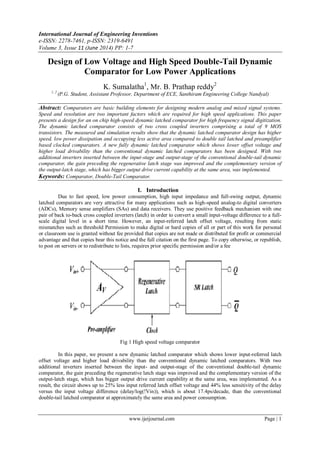
  • 1. International Journal of Engineering Inventions e-ISSN: 2278-7461, p-ISSN: 2319-6491 Volume 3, Issue 11 (June 2014) PP: 1-7 www.ijeijournal.com Page | 1 Design of Low Voltage and High Speed Double-Tail Dynamic Comparator for Low Power Applications K. Sumalatha1 , Mr. B. Prathap reddy2 1, 2 (P.G. Student, Assistant Professor, Department of ECE, Santhiram Engineering College Nandyal) Abstract: Comparators are basic building elements for designing modern analog and mixed signal systems. Speed and resolution are two important factors which are required for high speed applications. This paper presents a design for an on chip high-speed dynamic latched comparator for high frequency signal digitization. The dynamic latched comparator consists of two cross coupled inverters comprising a total of 9 MOS transistors. The measured and simulation results show that the dynamic latched comparator design has higher speed, low power dissipation and occupying less active area compared to double tail latched and preamplifier based clocked comparators. A new fully dynamic latched comparator which shows lower offset voltage and higher load drivability than the conventional dynamic latched comparators has been designed. With two additional inverters inserted between the input-stage and output-stage of the conventional double-tail dynamic comparator, the gain preceding the regenerative latch stage was improved and the complementary version of the output-latch stage, which has bigger output drive current capability at the same area, was implemented. Keywords: Comparator, Double-Tail Comparator. I. Introduction Due to fast speed, low power consumption, high input impedance and full-swing output, dynamic latched comparators are very attractive for many applications such as high-speed analog-to digital converters (ADCs), Memory sense amplifiers (SAs) and data receivers. They use positive feedback mechanism with one pair of back to-back cross coupled inverters (latch) in order to convert a small input-voltage difference to a full- scale digital level in a short time. However, an input-referred latch offset voltage, resulting from static mismatches such as threshold Permission to make digital or hard copies of all or part of this work for personal or classroom use is granted without fee provided that copies are not made or distributed for profit or commercial advantage and that copies bear this notice and the full citation on the first page. To copy otherwise, or republish, to post on servers or to redistribute to lists, requires prior specific permission and/or a fee Fig 1 High speed voltage comparator In this paper, we present a new dynamic latched comparator which shows lower input-referred latch offset voltage and higher load drivability than the conventional dynamic latched comparators. With two additional inverters inserted between the input- and output-stage of the conventional double-tail dynamic comparator, the gain preceding the regenerative latch stage was improved and the complementary version of the output-latch stage, which has bigger output drive current capability at the same area, was implemented. As a result, the circuit shows up to 25% less input referred latch offset voltage and 44% less sensitivity of the delay versus the input voltage difference (delay/log(!Vin)), which is about 17.4ps/decade, than the conventional double-tail latched comparator at approximately the same area and power consumption.
  • 2. Design Of Low Voltage And High Speed Double-Tail Dynamic Comparator For Low Power www.ijeijournal.com Page | 2 II. Clockedregenerative Comparators Clocked regenerative comparators have found wide applications in many high-speed ADCs since they can make fast decisions due to the strong positive feedback in the regenerative latch. Recently, many comprehensive analyses have been presented, which investigate the performance of these comparators from different aspects, such as noise [11], offset [12], [13], and [14], random decision errors [15], and kick-back noise [16]. In this section, a comprehensive delay analysis is presented; the delay time of two common structures, i.e., conventional dynamic comparator and conventional dynamic double-tail comparator are analyzed, based on which the proposed comparator will be presented. A. Conventional Dynamic Comparator The schematic diagram of the conventional dynamic comparator widely used in A/D converters, with high input impedance, rail-to-rail output swing, and no static power consumption is shown in Fig. 1 [1], [17]. The operation of the comparator is as follows. During the reset phase when CLK = 0 and Mtail is off, reset transistors (M7–M8) pull both output nodes Outn and Outp to VDD to define a start condition and to have a valid logical level during reset. In the comparison phase, when CLK = VDD, transistors M7 and M8 are off, and Mtail is on. Output voltages (Outp, Outn), which had been pre-charged to VDD, start to discharge with different discharging rates depending on the corresponding input voltage (INN/INP). Assuming the case where VINP > VINN, Outp discharges faster than Outn, hence when Outp (discharged by transistor M2 drain current), falls down to VDD–|Vthp| before Outn (discharged by transistor M1 drain current), the corresponding pMOS transistor (M5) will turn on initiating the latch regeneration caused by back-to-back inverters (M3, M5 and M4, M6). Thus, Outn pulls to VDD and Outp discharges to ground. If VINP < VINN, the circuits works viceversa. Fig2:Conventional Dynamic Comparator As shown in Fig. 2, the delay of this comparator is comprised of two time delays, t0 and tlatch. The delay t0 represents the capacitive discharge of the load capacitance CL until the first p-channel transistor (M5/M6) turns on. In case, the voltage at node INP is bigger than INN (i.e., VINP > VINN), the drain current of transistor M2 (I2) causes faster discharge of Outp node compared to the Outn node, which is driven by M1 with smaller current. Consequently, the discharge delay (t0) is given by In (1), since I2 = Itail/2 + _Iin = Itail/2 + gm1,2_Vin, for small differential input (_Vin), I2 can be approximated to be constant and equal to the half of the tail current. The second term, tlatch, is the latching delay of two crosscoupled inverters. It is assumed that a voltage swing of _Vout = VDD/2 has to be obtained from an initial output voltage difference _V0 at the falling output (e.g., Outp). Half of the supply voltage is considered to be the threshold voltage of the comparator following inverter or SR latch [17]. Hence, the latch delay time is given by, [18]
  • 3. Design Of Low Voltage And High Speed Double-Tail Dynamic Comparator For Low Power www.ijeijournal.com Page | 3 where gm,eff is the effective transconductance of the back-toback inverters. In fact, this delay depends, in a logarithmic manner, on the initial output voltage difference at the beginning of the regeneration (i.e., at t = t0). Based on (1), _V0 can be calculated from (3) The current difference, _Iin = |I1 − I2|, between the branches is much smaller than I1 and I2. Thus, I1 can be approximated by Itail/2 and (3) can be rewritten as In this equation, β1,2 is the input transistors’ current factor and Itail is a function of input common-mode voltage (Vcm) and VDD. Now, substituting _V0 in latch delay expression and considering t0, the expression for the delay of the conventional dynamic comparator is obtained as Equation (5) explains the impact of various parameters. The total delay is directly proportional to the comparator load capacitance CL and inversely proportional to the input difference voltage (_Vin). Besides, the delay depends indirectly to the input common-mode voltage (Vcm). By reducing Vcm, the delay t0 of the first sensing phase increases because lower Vcm causes smaller bias current (Itail). On the other hand, (4) shows that a delayed discharge with smaller Itail results in an increased initial voltage difference (_V0), reducing tlatch. Simulation results show that the effect of reducing the Vcm on increasing of t0 and reducing of tlatch will finally lead to an increase in the total delay. In [17], it has been shown that an input common-mode voltage of 70% of the supply voltage is optimal regarding speed and yield. Fig 3: Schematic diagram of the conventional double-tail dynamic comparator.
  • 4. Design Of Low Voltage And High Speed Double-Tail Dynamic Comparator For Low Power www.ijeijournal.com Page | 4 B. Conventional Double-Tail Dynamic Comparator A conventional double-tail comparator is shown in Fig. 3 [10]. This topology has less stacking and therefore can operate at lower supply voltages compared to the conventional dynamic comparator. The double tail enables both a large current in the latching stage and wider Mtail2, for fast latching independent of the input common-mode voltage (Vcm), and a small current in the input stage (small Mtail1), for low Offset [10]. The operation of this comparator is as follows (see Fig. 4). During reset phase (CLK = 0, Mtail1, and Mtail2 are off), transistors M3-M4 pre-charge fn and fp nodes to VDD, which in turn causes transistors MR1 and MR2 to discharge the output nodes to ground. During decision-making phase (CLK = VDD, Mtail1 and Mtail2 turn on), M3-M4 turn off and voltages at nodes fn and fp start to drop with the rate defined by IMtail1/Cfn(p) and on top of this, an input-dependent differential voltage _Vfn(p) will build up. The intermediate stage formed by MR1 and MR2 passes _Vfn(p) to the crosscoupled inverters and also provides a good shielding between input and output, resulting in reduced value of kickback noise [10]. Similar to the conventional dynamic comparator, the delay of this comparator comprises two main parts, t0 and t latch. The delay t0 represents the capacitive charging of the load capacitance CL out (at the latch stage output nodes, Outn and Outp) until the first n-channel transistor (M9/M10) turns on, after which the latch regeneration starts; thus t0 is obtained. III. Proposed Double-Tail Dynamic Comparator Fig demonstrates the schematic diagram of the proposed dynamic double-tail comparator. Due to the better performance of double-tail architecture in low-voltage applications, the proposed comparator is designed based on the double-tail structure. The main idea of the proposed comparator is to increase _Vfn/fp in order to increase the latch regeneration speed. For this purpose, two control transistors (Mc1 and Mc2) have been added to the first stage in parallel to M3/M4 transistors but in a cross-coupled manner[see fig4]. Fig4: Proposed Dynamic Comparator main idea.
  • 5. Design Of Low Voltage And High Speed Double-Tail Dynamic Comparator For Low Power www.ijeijournal.com Page | 5 Fig5: Final structure of the proposed double-tail comparator . A. Operation of the Proposed Comparator The operation of the proposed comparator is as follows (see Fig.. During reset phase (CLK = 0, Mtail1 and Mtail2 are off, avoiding static power), M3 and M4 pulls both Fn and fp nodes to VDD, hence transistor Mc1 and Mc2 are cut off. Intermediate stage transistors, MR1 and MR2, reset both latch outputs to ground. During decision making phase (CLK = VDD, Mtail1, and Mtail2 are on), transistors M3 and M4 turn off. Furthermore, at the beginning of this phase, the control transistors are still off (since fn and fp are about VDD). Thus, fn and fp start to drop with different rates according to the input voltages. Suppose VINP > VINN, thus fn drops faster than fp, (since M2 provides more current than M1). As long as fn continues falling, the corresponding PMOS control transistor (Mc1 in this case) starts to turn on, pulling fp node back to the VDD; so another control transistor (Mc2) remains off, allowing fn to be discharged completely. In other words, unlike conventional double-tail dynamic comparator, in which _Vfn/fp is just a function of input transistor transconductance and input voltage difference (9), in the proposed structure as soon as the comparator detects that for instance node fn discharges faster, a PMOS transistor (Mc1) turns on, pulling the other node fp back to the VDD. Therefore by the time passing, the difference between fn and fp (_Vfn/fp) increases in an exponential manner, leading to the reduction of latch regeneration time (this will be shown in Section III-B). Despite the effectiveness of the proposed idea, one of the points which should be considered is that in this circuit, when one of the control transistors (e.g., Mc1) turns on, a current from VDD is drawn to the ground via input and tail transistor (e.g., Mc1, M1, and Mtail1), resulting in static power consumption. To overcome this issue, two NMOS switches are used below the input transistors [Msw1 and Msw2, as shown in Fig. 2(b)]. At the beginning of the decision making phase, due to the fact that both fn and fp nodes have been pre-charged to VDD. IV. Simulation Results In order to compare the proposed double-tail comparator with the conventional double –tail dynamic comparators,all circuits have been simulated in 0.12-μm CMOS technology.
  • 6. Design Of Low Voltage And High Speed Double-Tail Dynamic Comparator For Low Power www.ijeijournal.com Page | 6 Timing Diagram of Conventional Dynamic comparator Timing Diagram of Conventional double-tail comparator Timing diagram of proposed dynamic comparator
  • 7. Design Of Low Voltage And High Speed Double-Tail Dynamic Comparator For Low Power www.ijeijournal.com Page | 7 Timing Diagram of proposed Dynamic Comparator V. Conclusion: In this paper, we presented a comprehensive delay analysis for clocked dynamic comparators and expressions were derived. Two common structures of conventional dynamic comparator and conventional double-tail dynamic comparators were analyzed. Also, based on theoretical analyses, a new dynamic comparator with low-voltage low-power capability was proposed in order to improve the performance of the comparator. Post-layout simulation results in 0.12-μm CMOS technology confirmed that the delay and energy per conversion of the proposed comparator is reduced to a great extent in comparison with the conventional dynamic comparator and double-tail comparator. REFERENCES [1] B. Goll and H. Zimmermann, “A comparator with reduced delay time in 65-nm CMOS for supply voltages down to 0.65,” IEEE Trans. Circuits Syst. II, Exp. Briefs, vol. 56, no. 11, pp. 810–814, Nov. 2009. [2] S. U. Ay, “A sub-1 volt 10-bit supply boosted SAR ADC design in standard CMOS,” Int. J. Analog Integr. Circuits Signal Process., vol. 66, no. 2, pp. 213–221, Feb. 2011. [3] A. Mesgarani, M. N. Alam, F. Z. Nelson, and S. U. Ay, “Supply boosting technique for designing very low-voltage mixed-signal circuits in standard CMOS,” in Proc. IEEE Int. Midwest Symp. Circuits Syst. Dig. Tech. Papers, Aug. 2010, pp. 893–896. [4] B. J. Blalock, “Body-driving as a Low-Voltage Analog Design Technique for CMOS technology,” in Proc. IEEE Southwest Symp. Mixed-Signal Design, Feb. 2000, pp. 113– 118. [5] M. Maymandi-Nejad and M. Sachdev, “1-bit quantiser with rail to rail input range for sub-1V __ modulators,” IEEE Electron. Lett., vol. 39, no. 12, pp. 894–895, Jan. 2003. [6] K. Uyttenhove, M. S. J. Steyaert, "A 1.8-V, 6-bit, 1.3-GHz CMOS flash ADC in 0.25-_m CMOS," IEEE J. Solid-State Circuits, vol. 38, no. 7, pp.1115–1122, July 2003. [7] Jun He, Sanyi Zhan, Degang Chen, and R.L. Geiger, “Analyses of Static and Dynamic Random Offset Voltages in Dynamic Comparators,” IEEE Trans. Circuits Syst. I: Reg. Papers, vol. 56, pp. 911-919, May 2009. International AUTHORS 1. First Author K. Sumalatha, Received my Bachelor of Technology in Electronics and Communications in Vijay Institute Of Technology and Science, kama Reddy, her Research area is Design of low-voltage and high speed double-tail dynamic comparator for low power application under the guidance of Mr.B.Prathap reddy. Email: sumalathareddyece@gmail.com 2. Second Author Mr. B. Prathap Reddy, He is an assistant professor at the SREC, Nandyal, Kurnool, Andhra Pradesh, India. His research interests include VLSI, Embedded Systems. Email: prathap03_448@yahoo.co.in Correspondence Author:+91-9491515005