SlideShare une entreprise Scribd logo
1  sur  69
Télécharger pour lire hors ligne
M

PIC16F84A

18-pin Enhanced Flash/EEPROM 8-Bit Microcontroller

Devices Included in this Data Sheet:

Pin Diagrams

• PIC16F84A
• Extended voltage range device available
(PIC16LF84A)

PDIP, SOIC
RA1

17

RA0

3

16

OSC1/CLKIN

MCLR

4

15

OSC2/CLKOUT

VSS

5

14

VDD

RB0/INT

6

13

RB7

RB1

7

12

RB6

RB2

8

11

RB5

RB3

• Only 35 single word instructions to learn
• All instructions single cycle except for program
branches which are two-cycle
• Operating speed: DC - 20 MHz clock input
DC - 200 ns instruction cycle
• 1024 words of program memory
• 68 bytes of data RAM
• 64 bytes of data EEPROM
• 14-bit wide instruction words
• 8-bit wide data bytes
• 15 special function hardware registers
• Eight-level deep hardware stack
• Direct, indirect and relative addressing modes
• Four interrupt sources:
- External RB0/INT pin
- TMR0 timer overflow
- PORTB<7:4> interrupt on change
- Data EEPROM write complete

18

2

RA4/T0CKI

High Performance RISC CPU Features:

•1

RA3

9

10

RB4

SSOP
•1

20

RA1

RA3

2

19

RA0

RA4/T0CKI

3

18

OSC1/CLKIN

MCLR
VSS

4

17

OSC2/CLKOUT

16

VSS

6

RB0/INT

7

14

VDD
VDD
RB7

RB1

8

13

RB6

RB2

9
10

12
11

RB5

RB3

• 13 I/O pins with individual direction control
• High current sink/source for direct LED drive
- 25 mA sink max. per pin
- 25 mA source max. per pin
• TMR0: 8-bit timer/counter with 8-bit
programmable prescaler

5

PIC16F84A

RA2

Peripheral Features:

15

RB4

CMOS Enhanced Flash/EERPOM Technology:

Special Microcontroller Features:
• 1000 erase/write cycles Enhanced Flash program
memory
• 1,000,000 typical erase/write cycles EEPROM data
memory
• EEPROM Data Retention > 40 years
• In-Circuit Serial Programming (ICSP™) - via two
pins
• Power-on Reset (POR), Power-up Timer (PWRT),
Oscillator Start-up Timer (OST)
• Watchdog Timer (WDT) with its own on-chip RC
oscillator for reliable operation
• Code-protection
• Power saving SLEEP mode
• Selectable oscillator options

© 1998 Microchip Technology Inc.

PIC16F84A

RA2

• Low-power, high-speed technology
• Fully static design
• Wide operating voltage range:
- Commercial: 2.0V to 5.5V
- Industrial:
2.0V to 5.5V
• Low power consumption:
- < 2 mA typical @ 5V, 4 MHz
- 15 µA typical @ 2V, 32 kHz
- < 0.5 µA typical standby current @ 2V

Preliminary

DS35007A-page 1
PIC16F84A
Table of Contents
1.0 Device Overview ............................................................................................................................................................................ 3
2.0 Memory Organization..................................................................................................................................................................... 5
3.0 I/O Ports....................................................................................................................................................................................... 13
4.0 Timer0 Module ............................................................................................................................................................................. 17
5.0 Data EEPROM Memory............................................................................................................................................................... 19
6.0 Special Features of the CPU ....................................................................................................................................................... 21
7.0 Instruction Set Summary.............................................................................................................................................................. 33
8.0 Development Support .................................................................................................................................................................. 35
9.0 Electrical Characteristics for PIC16F84A..................................................................................................................................... 41
10.0 DC & AC Characteristics Graphs/Tables ..................................................................................................................................... 53
11.0 Packaging Information ................................................................................................................................................................. 55
Appendix A: Revision History ........................................................................................................................................................... 59
Appendix B: Conversion Considerations.......................................................................................................................................... 59
Appendix C: Migration from Baseline to Midrange Devices ............................................................................................................. 62
Index ................................................................................................................................................................................................... 63
On-Line Support................................................................................................................................................................................... 65
Reader Response ................................................................................................................................................................................ 66
PIC16F84A Product Identification System ........................................................................................................................................... 67

To Our Valued Customers
Most Current Data Sheet
To obtain the most up-to-date version of this data sheet, please check our Worldwide Web site at:
http://www.microchip.com
You can determine the version of a data sheet by examining its literature number found on the bottom outside corner of any page.
The last character of the literature number is the version number. e.g., DS30000A is version A of document DS30000.

Errata
An errata sheet may exist for current devices, describing minor operational differences (from the data sheet) and recommended
workarounds. As device/documentation issues become known to us, we will publish an errata sheet. The errata will specify the
revision of silicon and revision of document to which it applies.
To determine if an errata sheet exists for a particular device, please check with one of the following:
• Microchip’s Worldwide Web site; http://www.microchip.com
• Your local Microchip sales office (see last page)
• The Microchip Corporate Literature Center; U.S. FAX: (602) 786-7277
When contacting a sales office or the literature center, please specify which device, revision of silicon and data sheet (include literature number) you are using.

Corrections to this Data Sheet
We constantly strive to improve the quality of all our products and documentation. We have spent a great deal of time to ensure
that this document is correct. However, we realize that we may have missed a few things. If you find any information that is missing
or appears in error, please:
• Fill out and mail in the reader response form in the back of this data sheet.
• E-mail us at webmaster@microchip.com.
We appreciate your assistance in making this a better document.

DS35007A-page 2

Preliminary

© 1998 Microchip Technology Inc.
PIC16F84A
1.0

DEVICE OVERVIEW

The program memory contains 1K words, which translates to 1024 instructions, since each 14-bit program
memory word is the same width as each device instruction. The data memory (RAM) contains 68 bytes. Data
EEPROM is 64 bytes.

This document contains device-specific information for
the operation of the PIC16F84A device. Additional
information may be found in the PICmicro™ Mid-Range
Reference Manual, (DS33023), which may be downloaded from the Microchip website. The Reference
Manual should be considered a complementary document to this data sheet, and is highly recommended
reading for a better understanding of the device architecture and operation of the peripheral modules.

There are also 13 I/O pins that are user-configured on
a pin-to-pin basis. Some pins are multiplexed with other
device functions. These functions include:
• External interrupt
• Change on PORTB interrupt
• Timer0 clock input

The PIC16F84A belongs to the mid-range family of the
PICmicro™ microcontroller devices. A block diagram of
the device is shown in Figure 1-1.

FIGURE 1-1:

Table 1-1 details the pinout of the device with descriptions and details for each pin.

PIC16F84A BLOCK DIAGRAM
Data Bus

13

8

Program Counter

EEPROM Data Memory

Flash
Program
Memory
PIC16F84A
1K x 14
Program
Bus

8 Level Stack
(13-bit)

14

RAM
File Registers

EEDATA

PIC16F84A
68 x 8
7

RAM Addr

EEPROM
Data Memory
64 x 8

EEADR

Addr Mux

Instruction reg

7

Direct Addr

5

TMR0

Indirect
Addr

FSR reg
RA4/T0CKI
STATUS reg
8

MUX

Power-up
Timer
Instruction
Decode &
Control

Oscillator
Start-up Timer

8
ALU

Power-on
Reset
Watchdog
Timer

Timing
Generation

I/O Ports

RA3:RA0
W reg

RB7:RB1

RB0/INT

OSC2/CLKOUT
OSC1/CLKIN

MCLR

© 1998 Microchip Technology Inc.

VDD, VSS

Preliminary

DS35007A-page 3
PIC16F84A
TABLE 1-1

PIC16F84A PINOUT DESCRIPTION

Pin Name

DIP
No.

SOIC
No.

SSOP
No.

I/O/P
Type

Buffer
Type

OSC1/CLKIN

16

16

18

I

OSC2/CLKOUT

15

15

19

O

—

Oscillator crystal output. Connects to crystal or resonator in
crystal oscillator mode. In RC mode, OSC2 pin outputs
CLKOUT which has 1/4 the frequency of OSC1, and
denotes the instruction cycle rate.

MCLR

4

4

4

I/P

ST

Master clear (reset) input/programming voltage input. This
pin is an active low reset to the device.

RA0

17

17

19

I/O

TTL

RA1

18

18

20

I/O

TTL

RA2

1

1

1

I/O

TTL

RA3

2

2

2

I/O

TTL

RA4/T0CKI

3

3

3

I/O

ST

Description

ST/CMOS (3) Oscillator crystal input/external clock source input.

PORTA is a bi-directional I/O port.

Can also be selected to be the clock input to the TMR0
timer/counter. Output is open drain type.
PORTB is a bi-directional I/O port. PORTB can be software
programmed for internal weak pull-up on all inputs.

RB0/INT

6

6

7

I/O

RB1

7

7

8

I/O

TTL

RB2

8

8

9

I/O

TTL

RB3

9

9

10

I/O

TTL

RB4

10

10

11

I/O

TTL

RB5

11

11

12

I/O

RB0/INT can also be selected as an external interrupt
pin.

TTL/ST (1)

TTL

Interrupt on change pin.
(2)

RB6

12

12

13

I/O

TTL/ST

RB7

13

13

14

I/O

TTL/ST (2)

Interrupt on change pin. Serial programming clock.
Interrupt on change pin. Serial programming data.

VSS

5

5

5,6

P

—

Ground reference for logic and I/O pins.

VDD

14

14

15,16

P

—

Positive supply for logic and I/O pins.

Legend: I= input

O = output
I/O = Input/Output
P = power
— = Not used
TTL = TTL input
ST = Schmitt Trigger input
Note 1: This buffer is a Schmitt Trigger input when configured as the external interrupt.
2: This buffer is a Schmitt Trigger input when used in serial programming mode.
3: This buffer is a Schmitt Trigger input when configured in RC oscillator mode and a CMOS input otherwise.

DS35007A-page 4

Preliminary

© 1998 Microchip Technology Inc.
PIC16F84A
MEMORY ORGANIZATION

FIGURE 2-1:

There are two memory blocks in the PIC16F84A.
These are the program memory and the data memory.
Each block has its own bus, so that access to each
block can occur during the same oscillator cycle.
The data memory can further be broken down into the
general purpose RAM and the Special Function
Registers (SFRs). The operation of the SFRs that
control the “core” are described here. The SFRs used
to control the peripheral modules are described in the
section discussing each individual peripheral module.
The data memory area also contains the data
EEPROM memory. This memory is not directly mapped
into the data memory, but is indirectly mapped. That is,
an indirect address pointer specifies the address of the
data EEPROM memory to read/write. The 64 bytes of
data EEPROM memory have the address range
0h-3Fh. More details on the EEPROM memory can be
found in Section 5.0.

PROGRAM MEMORY MAP
AND STACK - PIC16F84A

PC<12:0>
13
CALL, RETURN
RETFIE, RETLW
Stack Level 1
•
•
•

Stack Level 8
Reset Vector

0000h

Peripheral Interrupt Vector

0004h

User Memory
Space

2.0

Additional information on device memory may be found
in the PICmicro™ Mid-Range Reference Manual,
(DS33023).

2.1

3FFh

Program Memory Organization

The PIC16FXX has a 13-bit program counter capable
of addressing an 8K x 14 program memory space.
For the PIC16F84A, the first 1K x 14 (0000h-03FFh)
are physically implemented (Figure 2-1). Accessing a
location above the physically implemented address will
cause a wraparound. For example, for locations 20h,
420h, 820h, C20h, 1020h, 1420h, 1820h, and 1C20h
will be the same instruction.

1FFFh

The reset vector is at 0000h and the interrupt vector is
at 0004h.

© 1998 Microchip Technology Inc.

Preliminary

DS35007A-page 5
PIC16F84A
2.2

Data Memory Organization

2.2.1

The data memory is partitioned into two areas. The first
is the Special Function Registers (SFR) area, while the
second is the General Purpose Registers (GPR) area.
The SFRs control the operation of the device.
Portions of data memory are banked. This is for both
the SFR area and the GPR area. The GPR area is
banked to allow greater than 116 bytes of general
purpose RAM. The banked areas of the SFR are for the
registers that control the peripheral functions. Banking
requires the use of control bits for bank selection.
These control bits are located in the STATUS Register.
Figure 2-1 shows the data memory map organization.

GENERAL PURPOSE REGISTER FILE

Each General Purpose Register (GPR) is 8 bits wide
and is accessed either directly or indirectly through the
FSR (Section 2.4).
The GPR addresses in bank 1 are mapped to
addresses in bank 0. As an example, addressing location 0Ch or 8Ch will access the same GPR.

FIGURE 2-1:

REGISTER FILE MAP PIC16F84A

File Address

File Address

00h

80h

TMR0

OPTION_REG

81h

02h

PCL

PCL

82h

03h

STATUS

STATUS

83h

04h

FSR

FSR

84h

05h

PORTA

TRISA

85h

06h

PORTB

TRISB

86h

08h

EEDATA

EECON1

88h

09h

EEADR

EECON2(1)

89h

0Ah

PCLATH

PCLATH

8Ah

0Bh

The entire data memory can be accessed either
directly using the absolute address of each register file
or indirectly through the File Select Register (FSR)
(Section 2.4). Indirect addressing uses the present
value of the RP0 bit for access into the banked areas of
data memory.

Indirect addr.(1)

01h

Instructions MOVWF and MOVF can move values from
the W register to any location in the register file (“F”),
and vice-versa.

Indirect addr.(1)

INTCON

INTCON

8Bh

87h

07h

Data memory is partitioned into two banks which
contain the general purpose registers and the special
function registers. Bank 0 is selected by clearing the
RP0 bit (STATUS<5>). Setting the RP0 bit selects Bank
1. Each Bank extends up to 7Fh (128 bytes). The first
twelve locations of each Bank are reserved for the
Special Function Registers. The remainder are General Purpose Registers implemented as static RAM.

8Ch

0Ch

68
General
Purpose
Registers
(SRAM)

Mapped
(accesses)
in Bank 0

4Fh
50h

CFh
D0h

FFh

7Fh
Bank 0

Bank 1

Unimplemented data memory location; read as '0'.
Note 1: Not a physical register.

DS35007A-page 6

Preliminary

© 1998 Microchip Technology Inc.
PIC16F84A
2.2.2

The special function registers can be classified into two
sets, core and peripheral. Those associated with the
core functions are described in this section. Those
related to the operation of the peripheral features are
described in the section for that specific feature.

SPECIAL FUNCTION REGISTERS

The Special Function Registers (Figure 2-1 and
Table 2-1) are used by the CPU and Peripheral
functions to control the device operation. These
registers are static RAM.

TABLE 2-1

Addr

REGISTER FILE SUMMARY

Name

Bit 7

Bit 6

Bit 5

Bit 4

Bit 3

Bit 2

Bit 1

Bit 0

Value on
Power-on
Reset

Value on all
other resets
(Note3)

Bank 0
00h

INDF

Uses contents of FSR to address data memory (not a physical register)

---- ----

---- ----

01h

TMR0

8-bit real-time clock/counter

xxxx xxxx

uuuu uuuu

02h

PCL

Low order 8 bits of the Program Counter (PC)

0000 0000

0000 0000

0001 1xxx

000q quuu

(2)

03h

STATUS

04h

FSR

05h

PORTA (4)

06h

PORTB (5)

IRP

RP1

TO

RP0

PD

Z

DC

C

Indirect data memory address pointer 0

xxxx xxxx

—

—

—

RA4/T0CKI

RA3

RA2

RA1

RA0

RB7

RB6

RB5

RB4

RB3

RB2

RB1

RB0/INT

uuuu uuuu

---x xxxx

---u uuuu

xxxx xxxx

uuuu uuuu

Unimplemented location, read as '0'

07h

---- ----

---- ----

xxxx xxxx

uuuu uuuu

xxxx xxxx

uuuu uuuu

---0 0000

---0 0000

0000 000x

0000 000u

---- ----

---- ----

1111 1111

1111 1111

08h

EEDATA

EEPROM data register

09h

EEADR

EEPROM address register

0Ah

PCLATH

—

—

—

0Bh

INTCON

GIE

EEIE

Write buffer for upper 5 bits of the PC (1)

T0IE

INTE

RBIE

T0IF

INTF

RBIF

Bank 1
80h

INDF

81h

OPTION_REG

82h

PCL

83h

STATUS (2)

84h

FSR

85h

TRISA

86h

TRISB

Uses contents of FSR to address data memory (not a physical register)
RBPU

INTEDG

T0CS

T0SE

PSA

PS2

PS1

PS0

Low order 8 bits of Program Counter (PC)
IRP

RP1

RP0

TO

0000 0000
Z

DC

C

Indirect data memory address pointer 0
—

—

—

PORTA data direction register

0000 0000

0001 1xxx

000q quuu

xxxx xxxx

PD

uuuu uuuu
---1 1111

PORTB data direction register

1111 1111

1111 1111

Unimplemented location, read as '0'

87h

---1 1111

---- ----

---- ----

88h

EECON1

89h

EECON2

—

—

—

0Ah

PCLATH

—

—

—

0Bh

INTCON

GIE

EEIE

T0IE

EEIF

WRERR

WREN

WR

RD

INTE

RBIE

T0IF

INTF

RBIF

---0 q000
---- ----

---0 0000

Write buffer for upper 5 bits of the PC (1)

---0 x000
---- ----

EEPROM control register 2 (not a physical register)

---0 0000

0000 000x

0000 000u

Legend: x = unknown, u = unchanged. - = unimplemented read as '0', q = value depends on condition.
Note 1: The upper byte of the program counter is not directly accessible. PCLATH is a slave register for PC<12:8>. The contents
of PCLATH can be transferred to the upper byte of the program counter, but the contents of PC<12:8> is never transferred
to PCLATH.
2: The TO and PD status bits in the STATUS register are not affected by a MCLR reset.
3: Other (non power-up) resets include: external reset through MCLR and the Watchdog Timer Reset.
4: On any device reset, these pins are configured as inputs.
5: This is the value that will be in the port output latch.

© 1998 Microchip Technology Inc.

Preliminary

DS35007A-page 7
PIC16F84A
2.2.2.1

STATUS REGISTER

The STATUS register contains the arithmetic status of
the ALU, the RESET status and the bank select bit for
data memory.
As with any register, the STATUS register can be the
destination for any instruction. If the STATUS register is
the destination for an instruction that affects the Z, DC
or C bits, then the write to these three bits is disabled.
These bits are set or cleared according to device logic.
Furthermore, the TO and PD bits are not writable.
Therefore, the result of an instruction with the STATUS
register as destination may be different than intended.
For example, CLRF STATUS will clear the upper-three
bits and set the Z bit. This leaves the STATUS register
as 000u u1uu (where u = unchanged).

FIGURE 2-1:
R/W-0
IRP
bit7

bit 7:

Only the BCF, BSF, SWAPF and MOVWF instructions
should be used to alter the STATUS register (Table 7-2)
because these instructions do not affect any status bit.
Note 1: The IRP and RP1 bits (STATUS<7:6>) are
not used by the PIC16F84A and should be
programmed as cleared. Use of these bits
as general purpose R/W bits is NOT
recommended, since this may affect
upward compatibility with future products.
Note 2: The C and DC bits operate as a borrow
and digit borrow out bit, respectively, in
subtraction. See the SUBLW and SUBWF
instructions for examples.
Note 3: When the STATUS register is the
destination for an instruction that affects
the Z, DC or C bits, then the write to these
three bits is disabled. The specified bit(s)
will be updated according to device logic

STATUS REGISTER (ADDRESS 03h, 83h)

R/W-0
RP1

R/W-0
RP0

R-1
TO

R-1
PD

R/W-x
Z

R/W-x
DC

R/W-x
C
bit0

R = Readable bit
W = Writable bit
U = Unimplemented bit,
read as ‘0’
- n = Value at POR reset

IRP: Register Bank Select bit (used for indirect addressing)
The IRP bit is not used by the PIC16F84A. IRP should be maintained clear.

bit 6-5: RP1:RP0: Register Bank Select bits (used for direct addressing)
00 = Bank 0 (00h - 7Fh)
01 = Bank 1 (80h - FFh)
Each bank is 128 bytes. Only bit RP0 is used by the PIC16F84A. RP1 should be maintained clear.
bit 4:

TO: Time-out bit
1 = After power-up, CLRWDT instruction, or SLEEP instruction
0 = A WDT time-out occurred

bit 3:

PD: Power-down bit
1 = After power-up or by the CLRWDT instruction
0 = By execution of the SLEEP instruction

bit 2:

Z: Zero bit
1 = The result of an arithmetic or logic operation is zero
0 = The result of an arithmetic or logic operation is not zero

bit 1:

DC: Digit carry/borrow bit (for ADDWF and ADDLW instructions) (For borrow the polarity is reversed)
1 = A carry-out from the 4th low order bit of the result occurred
0 = No carry-out from the 4th low order bit of the result

bit 0:

C: Carry/borrow bit (for ADDWF and ADDLW instructions)
1 = A carry-out from the most significant bit of the result occurred
0 = No carry-out from the most significant bit of the result occurred
Note:For borrow the polarity is reversed. A subtraction is executed by adding the two’s complement of
the second operand. For rotate (RRF, RLF) instructions, this bit is loaded with either the high or low
order bit of the source register.

DS35007A-page 8

Preliminary

© 1998 Microchip Technology Inc.
PIC16F84A
2.2.2.2

OPTION_REG REGISTER

The OPTION_REG register is a readable and writable
register which contains various control bits to configure
the TMR0/WDT prescaler, the external INT interrupt,
TMR0, and the weak pull-ups on PORTB.

FIGURE 2-1:
R/W-1
RBPU
bit7

Note:

When the prescaler is assigned to
the WDT (PSA = '1'), TMR0 has a 1:1
prescaler assignment.

OPTION_REG REGISTER (ADDRESS 81h)

R/W-1
INTEDG

R/W-1
T0CS

R/W-1
T0SE

R/W-1
PSA

R/W-1
PS2

R/W-1
PS1

R/W-1
PS0
bit0

bit 7:

RBPU: PORTB Pull-up Enable bit
1 = PORTB pull-ups are disabled
0 = PORTB pull-ups are enabled (by individual port latch values)

bit 6:

INTEDG: Interrupt Edge Select bit
1 = Interrupt on rising edge of RB0/INT pin
0 = Interrupt on falling edge of RB0/INT pin

bit 5:

T0CS: TMR0 Clock Source Select bit
1 = Transition on RA4/T0CKI pin
0 = Internal instruction cycle clock (CLKOUT)

bit 4:

T0SE: TMR0 Source Edge Select bit
1 = Increment on high-to-low transition on RA4/T0CKI pin
0 = Increment on low-to-high transition on RA4/T0CKI pin

bit 3:

R = Readable bit
W = Writable bit
U = Unimplemented bit,
read as ‘0’
- n = Value at POR reset

PSA: Prescaler Assignment bit
1 = Prescaler assigned to the WDT
0 = Prescaler assigned to TMR0

bit 2-0: PS2:PS0: Prescaler Rate Select bits
Bit Value

TMR0 Rate

WDT Rate

000
001
010
011
100
101
110
111

1:2
1:4
1:8
1 : 16
1 : 32
1 : 64
1 : 128
1 : 256

1:1
1:2
1:4
1:8
1 : 16
1 : 32
1 : 64
1 : 128

© 1998 Microchip Technology Inc.

Preliminary

DS35007A-page 9
PIC16F84A
2.2.2.3

INTCON REGISTER

The INTCON register is a readable and writable
register which contains the various enable bits for all
interrupt sources.

FIGURE 2-1:
R/W-0
GIE
bit7

bit 7:

Note:

Interrupt flag bits get set when an interrupt
condition occurs regardless of the state of
its corresponding enable bit or the global
enable bit, GIE (INTCON<7>).

INTCON REGISTER (ADDRESS 0Bh, 8Bh)

R/W-0
EEIE

R/W-0
T0IE

R/W-0
INTE

R/W-0
RBIE

R/W-0
T0IF

R/W-0
INTF

R/W-x
RBIF
bit0

R = Readable bit
W = Writable bit
U = Unimplemented bit,
read as ‘0’
- n = Value at POR reset

GIE: Global Interrupt Enable bit
1 = Enables all un-masked interrupts
0 = Disables all interrupts
Note: For the operation of the interrupt structure, please refer to Section •.

bit 6:

EEIE: EE Write Complete Interrupt Enable bit
1 = Enables the EE write complete interrupt
0 = Disables the EE write complete interrupt

bit 5:

T0IE: TMR0 Overflow Interrupt Enable bit
1 = Enables the TMR0 interrupt
0 = Disables the TMR0 interrupt

bit 4:

INTE: RB0/INT Interrupt Enable bit
1 = Enables the RB0/INT interrupt
0 = Disables the RB0/INT interrupt

bit 3:

RBIE: RB Port Change Interrupt Enable bit
1 = Enables the RB port change interrupt
0 = Disables the RB port change interrupt

bit 2:

T0IF: TMR0 Overflow Interrupt Flag bit
1 = TMR0 has overflowed (must be cleared in software)
0 = TMR0 did not overflow

bit 1:

INTF: RB0/INT Interrupt Flag bit
1 = The RB0/INT interrupt occurred
0 = The RB0/INT interrupt did not occur

bit 0:

RBIF: RB Port Change Interrupt Flag bit
1 = When at least one of the RB7:RB4 pins changed state (must be cleared in software)
0 = None of the RB7:RB4 pins have changed state

DS35007A-page 10

Preliminary

© 1998 Microchip Technology Inc.
PIC16F84A
2.3

PCL and PCLATH

2.4

The program counter (PC) specifies the address of the
instruction to fetch for execution. The PC is 13 bits
wide. The low byte is called the PCL register. This register is readable and writable. The high byte is called
the PCH register. This register contains the PC<12:8>
bits and is not directly readable or writable. All updates
to the PCH register go through the PCLATH register.
2.3.1

STACK

The stack allows a combination of up to 8 program calls
and interrupts to occur. The stack contains the return
address from this branch in program execution.
Midrange devices have an 8 level deep x 13-bit wide
hardware stack. The stack space is not part of either
program or data space and the stack pointer is not
readable or writable. The PC is PUSHed onto the stack
when a CALL instruction is executed or an interrupt
causes a branch. The stack is POPed in the event of a
RETURN, RETLW or a RETFIE instruction execution.
PCLATH is not modified when the stack is PUSHed or
POPed.
After the stack has been PUSHed eight times, the ninth
push overwrites the value that was stored from the first
push. The tenth push overwrites the second push (and
so on).

Indirect Addressing; INDF and FSR
Registers

The INDF register is not a physical register. Addressing INDF actually addresses the register whose
address is contained in the FSR register (FSR is a
pointer). This is indirect addressing.

EXAMPLE 2-1:

INDIRECT ADDRESSING

•
•
•
•

Register file 05 contains the value 10h
Register file 06 contains the value 0Ah
Load the value 05 into the FSR register
A read of the INDF register will return the value of
10h
• Increment the value of the FSR register by one
(FSR = 06)
• A read of the INDF register now will return the
value of 0Ah.
Reading INDF itself indirectly (FSR = 0) will produce
00h. Writing to the INDF register indirectly results in a
no-operation (although STATUS bits may be affected).
A simple program to clear RAM locations 20h-2Fh
using indirect addressing is shown in Example 2-2.

EXAMPLE 2-2:

NEXT

movlw
movwf
clrf
incf
btfss
goto

HOW TO CLEAR RAM
USING INDIRECT
ADDRESSING
0x20
FSR
INDF
FSR
FSR,4
NEXT

;initialize pointer
; to RAM
;clear INDF register
;inc pointer
;all done?
;NO, clear next

CONTINUE
:

;YES, continue

An effective 9-bit address is obtained by concatenating
the 8-bit FSR register and the IRP bit (STATUS<7>), as
shown in Figure 2-1. However, IRP is not used in the
PIC16F84A.

© 1998 Microchip Technology Inc.

Preliminary

DS35007A-page 11
PIC16F84A
FIGURE 2-1:

DIRECT/INDIRECT ADDRESSING
Indirect Addressing

Direct Addressing
RP1 RP0

6

0

from opcode

IRP

(2)

bank select

7

(FSR)

0

(2)

location select

bank select

00

location select

01

00h

80h

0Bh
0Ch
Addresses
map back
to Bank 0

Data
Memory (1)
4Fh
50h

(3)

(3)

7Fh

FFh
Bank 0

Bank 1

Note 1: For memory map detail see Figure 2-1.
2: Maintain as clear for upward compatiblity with future products.
3: Not implemented.

DS35007A-page 12

Preliminary

© 1998 Microchip Technology Inc.
PIC16F84A
3.0

I/O PORTS

FIGURE 3-1:

Some pins for these I/O ports are multiplexed with an
alternate function for the peripheral features on the
device. In general, when a peripheral is enabled, that
pin may not be used as a general purpose I/O pin.
Additional information on I/O ports may be found in the
PICmicro™
Mid-Range
Reference
Manual,
(DS33023).

BLOCK DIAGRAM OF PINS
RA3:RA0

Data
bus
D
WR
Port

Q
VDD

CK

Q

P

Data Latch

3.1

PORTA and TRISA Registers

N

PORTA is a 5-bit wide bi-directional port. The corresponding data direction register is TRISA. Setting a
TRISA bit (=1) will make the corresponding PORTA pin
an input, i.e., put the corresponding output driver in a
hi-impedance mode. Clearing a TRISA bit (=0) will
make the corresponding PORTA pin an output, i.e., put
the contents of the output latch on the selected pin.
Note:

D
WR
TRIS

Reading the PORTA register reads the status of the
pins whereas writing to it will write to the port latch. All
write operations are read-modify-write operations.
Therefore a write to a port implies that the port pins are
read, this value is modified, and then written to the port
data latch.
Pin RA4 is multiplexed with the Timer0 module clock
input to become the RA4/T0CKI pin. The RA4/T0CKI
pin is a Schmitt Trigger input and an open drain output.
All other RA port pins have TTL input levels and full
CMOS output drivers.

EXAMPLE 3-1:

VSS
CK

Q

TRIS Latch

On a Power-on Reset, these pins are configured as inputs and read as '0'.

I/O pin

Q

TTL
input
buffer

RD TRIS
Q

D

EN
RD PORT

Note: I/O pins have protection diodes to VDD and VSS.

INITIALIZING PORTA

BCF
CLRF

STATUS, RP0
PORTA

BSF
MOVLW

STATUS, RP0
0x0F

MOVWF

TRISA

;
;
;
;
;
;
;
;
;
;
;
;

Initialize PORTA by
clearing output
data latches
Select Bank 1
Value used to
initialize data
direction
Set RA<3:0> as inputs
RA4 as output
TRISA<7:5> are always
read as '0'.

© 1998 Microchip Technology Inc.

Preliminary

DS35007A-page 13
PIC16F84A
FIGURE 3-2:

BLOCK DIAGRAM OF PIN RA4

Data
bus

D

Q

CK

WR
PORT

Q

RA4 pin

N
Data Latch
VSS
D

CK

WR
TRIS

Q
Q

Schmitt
Trigger
input
buffer

TRIS Latch

RD TRIS
Q

D
EN
EN

RD PORT
TMR0 clock input
Note: I/O pin has protection diodes to VSS only.

TABLE 3-1

PORTA FUNCTIONS

Name

Bit0

Buffer Type

RA0
RA1
RA2
RA3
RA4/T0CKI

bit0
bit1
bit2
bit3
bit4

TTL
TTL
TTL
TTL
ST

Function

Input/output
Input/output
Input/output
Input/output
Input/output or external clock input for TMR0.
Output is open drain type.
Legend: TTL = TTL input, ST = Schmitt Trigger input

TABLE 3-2

SUMMARY OF REGISTERS ASSOCIATED WITH PORTA

Address

Name

Bit 7

Bit 6

Bit 5

Bit 4

Bit 3

Bit 2

05h

PORTA

—

—

—

RA4/T0CKI

RA3

RA2

85h

TRISA

—

—

—

TRISA4

TRISA3

TRISA2

Bit 0

Value on
Power-on
Reset

Value on all
other resets

RA1

RA0

---x xxxx

---u uuuu

TRISA1

TRISA0

---1 1111

---1 1111

Bit 1

Legend: x = unknown, u = unchanged, - = unimplemented read as '0'. Shaded cells are unimplemented, read as '0'

DS35007A-page 14

Preliminary

© 1998 Microchip Technology Inc.
PIC16F84A
3.2

PORTB and TRISB Registers

PORTB is an 8-bit wide bi-directional port. The corresponding data direction register is TRISB. Setting a
TRISB bit (=1) will make the corresponding PORTB pin
an input, i.e., put the corresponding output driver in a
hi-impedance mode. Clearing a TRISB bit (=0) will
make the corresponding PORTB pin an output, i.e., put
the contents of the output latch on the selected pin.

EXAMPLE 3-1:
BCF
CLRF

BSF
MOVLW

MOVWF

INITIALIZING PORTB

STATUS, RP0
PORTB

;
;
;
;
;
;
;
;
;
;
;

STATUS, RP0
0xCF

TRISB

Initialize PORTB by
clearing output
data latches
Select Bank 1
Value used to
initialize data
direction
Set RB<3:0> as inputs
RB<5:4> as outputs
RB<7:6> as inputs

Each of the PORTB pins has a weak internal pull-up. A
single control bit can turn on all the pull-ups. This is performed by clearing bit RBPU (OPTION<7>). The weak
pull-up is automatically turned off when the port pin is
configured as an output. The pull-ups are disabled on a
Power-on Reset.

FIGURE 3-3:

Four of PORTB’s pins, RB7:RB4, have an interrupt on
change feature. Only pins configured as inputs can
cause this interrupt to occur (i.e. any RB7:RB4 pin configured as an output is excluded from the interrupt on
change comparison). The input pins (of RB7:RB4) are
compared with the old value latched on the last read of
PORTB. The “mismatch” outputs of RB7:RB4 are
OR’ed together to generate the RB Port Change Interrupt with flag bit RBIF (INTCON<0>).
This interrupt can wake the device from SLEEP. The
user, in the interrupt service routine, can clear the interrupt in the following manner:
a)
b)

Any read or write of PORTB. This will end the
mismatch condition.
Clear flag bit RBIF.

A mismatch condition will continue to set flag bit RBIF.
Reading PORTB will end the mismatch condition, and
allow flag bit RBIF to be cleared.
The interrupt on change feature is recommended for
wake-up on key depression operation and operations
where PORTB is only used for the interrupt on change
feature. Polling of PORTB is not recommended while
using the interrupt on change feature.

FIGURE 3-4:

BLOCK DIAGRAM OF PINS
RB3:RB0
VDD

BLOCK DIAGRAM OF PINS
RB7:RB4

RBPU(1)

Data bus

weak
P pull-up
Data Latch
D
Q

VDD
RBPU(1)

Data bus

weak
P pull-up

WR Port

TRIS Latch
D
Q

Data Latch
D

WR Port

Q
I/O
pin(2)

CK

I/O
pin(2)

CK

WR TRIS

TTL
Input
Buffer

CK

TRIS Latch
D
WR TRIS

Q

RD TRIS
TTL
Input
Buffer

CK

Q
RD Port

Latch

RD TRIS

Q
RD Port

D
EN

RB0/INT
D

Schmitt Trigger
Buffer

EN

RD Port

Note 1: TRISB = '1' enables weak pull-up
(if RBPU = '0' in the OPTION_REG register).

Set RBIF

2: I/O pins have diode protection to VDD and VSS.
From other
RB7:RB4 pins

Q

D
EN
RD Port

Note 1: TRISB = '1' enables weak pull-up
(if RBPU = '0' in the OPTION_REG register).
2: I/O pins have diode protection to VDD and VSS.

© 1998 Microchip Technology Inc.

Preliminary

DS35007A-page 15
PIC16F84A
TABLE 3-3

PORTB FUNCTIONS

Name

Bit

Buffer Type

I/O Consistency Function

TTL/ST(1)

Input/output pin or external interrupt input. Internal software
programmable weak pull-up.
RB1
bit1
TTL
Input/output pin. Internal software programmable weak pull-up.
RB2
bit2
TTL
Input/output pin. Internal software programmable weak pull-up.
RB3
bit3
TTL
Input/output pin. Internal software programmable weak pull-up.
RB4
bit4
TTL
Input/output pin (with interrupt on change). Internal software programmable
weak pull-up.
RB5
bit5
TTL
Input/output pin (with interrupt on change). Internal software programmable
weak pull-up.
RB6
bit6
TTL/ST(2)
Input/output pin (with interrupt on change). Internal software programmable
weak pull-up. Serial programming clock.
RB7
bit7
TTL/ST(2)
Input/output pin (with interrupt on change). Internal software programmable
weak pull-up. Serial programming data.
Legend: TTL = TTL input, ST = Schmitt Trigger.
Note 1: This buffer is a Schmitt Trigger input when configured as the external interrupt.
2: This buffer is a Schmitt Trigger input when used in serial programming mode.
RB0/INT

bit0

TABLE 3-4
Addr

SUMMARY OF REGISTERS ASSOCIATED WITH PORTB

Name

Bit 7

Bit 6

Bit 5

Bit 4

Bit 3

Bit 2

Bit 1

Bit 0

Value on
Power-on
Reset

Value on all
other resets

06h

PORTB

RB7

RB6

RB5

RB4

RB3

RB2

RB1

RB0/INT

xxxx xxxx

uuuu uuuu

86h

TRISB

TRISB7

TRISB6

TRISB5

TRISB4

TRISB3

TRISB2

TRISB1

TRISB0

1111 1111

1111 1111

81h

OPTION_REG

RBPU

INTEDG

T0CS

T0SE

PSA

PS2

PS1

PS0

1111 1111

1111 1111

Legend: x = unknown, u = unchanged. Shaded cells are not used by PORTB.

DS35007A-page 16

Preliminary

© 1998 Microchip Technology Inc.
PIC16F84A
4.0

TIMER0 MODULE

Additional information on external clock requirements
is available in the PICmicro™ Mid-Range Reference
Manual, (DS33023).

The Timer0 module timer/counter has the following features:
•
•
•
•
•
•

4.2

8-bit timer/counter
Readable and writable
Internal or external clock select
Edge select for external clock
8-bit software programmable prescaler
Interrupt on overflow from FFh to 00h

An 8-bit counter is available as a prescaler for the
Timer0 module, or as a postscaler for the Watchdog
Timer, respectively (Figure 4-2). For simplicity, this
counter is being referred to as “prescaler” throughout
this data sheet. Note that there is only one prescaler
available which is mutually exclusively shared between
the Timer0 module and the Watchdog Timer. Thus, a
prescaler assignment for the Timer0 module means
that there is no prescaler for the Watchdog Timer, and
vice-versa.

Figure 4-1 is a simplified block diagram of the Timer0
module.
Additional information on timer modules is available in
the PICmicro™ Mid-Range Reference Manual,
(DS33023).

4.1

The prescaler is not readable or writable.
The PSA and PS2:PS0 bits (OPTION_REG<3:0>)
determine the prescaler assignment and prescale ratio.

Timer0 Operation

Timer0 can operate as a timer or as a counter.

Clearing bit PSA will assign the prescaler to the Timer0
module. When the prescaler is assigned to the Timer0
module, prescale values of 1:2, 1:4, ..., 1:256 are
selectable.

Timer mode is selected by clearing bit T0CS
(OPTION_REG<5>). In timer mode, the Timer0 module will increment every instruction cycle (without prescaler). If the TMR0 register is written, the increment is
inhibited for the following two instruction cycles. The
user can work around this by writing an adjusted value
to the TMR0 register.

Setting bit PSA will assign the prescaler to the Watchdog Timer (WDT). When the prescaler is assigned to
the WDT, prescale values of 1:1, 1:2, ..., 1:128 are
selectable.

Counter mode is selected by setting bit T0CS
(OPTION_REG<5>). In counter mode, Timer0 will
increment either on every rising or falling edge of pin
RA4/T0CKI. The incrementing edge is determined by
the Timer0 Source Edge Select bit T0SE
(OPTION_REG<4>). Clearing bit T0SE selects the rising edge. Restrictions on the external clock input are
discussed below.

When assigned to the Timer0 module, all instructions
writing to the TMR0 register (e.g. CLRF 1, MOVWF 1,
BSF
1,x....etc.) will clear the prescaler. When
assigned to WDT, a CLRWDT instruction will clear the
prescaler along with the WDT.
Note:

When an external clock input is used for Timer0, it must
meet certain requirements. The requirements ensure
the external clock can be synchronized with the internal
phase clock (TOSC). Also, there is a delay in the actual
incrementing of Timer0 after synchronization.

FIGURE 4-1:

Prescaler

Writing to TMR0 when the prescaler is
assigned to Timer0 will clear the prescaler
count, but will not change the prescaler
assignment.

TIMER0 BLOCK DIAGRAM
Data bus
FOSC/4

0

PSout
1

1
Programmable
Prescaler

RA4/T0CKI
pin

0

8
Sync with
Internal
clocks

TMR0
PSout

(2 cycle delay)

T0SE
3
PS2, PS1, PS0

PSA

T0CS

Set interrupt
flag bit T0IF
on overflow

Note 1: T0CS, T0SE, PSA, PS2:PS0 (OPTION_REG<5:0>).
2: The prescaler is shared with Watchdog Timer (refer to Figure 4-2 for detailed block diagram).

© 1998 Microchip Technology Inc.

Preliminary

DS35007A-page 17
PIC16F84A
4.2.1

4.3

SWITCHING PRESCALER ASSIGNMENT

The prescaler assignment is fully under software control, i.e., it can be changed “on the fly” during program
execution.
Note:

The TMR0 interrupt is generated when the TMR0 register overflows from FFh to 00h. This overflow sets bit
T0IF (INTCON<2>). The interrupt can be masked by
clearing bit T0IE (INTCON<5>). Bit T0IF must be
cleared in software by the Timer0 module interrupt service routine before re-enabling this interrupt. The
TMR0 interrupt cannot awaken the processor from
SLEEP since the timer is shut off during SLEEP.

To avoid an unintended device RESET, a
specific instruction sequence (shown in the
PICmicro™ Mid-Range Reference Manual, DS3023) must be executed when
changing the prescaler assignment from
Timer0 to the WDT. This sequence must be
followed even if the WDT is disabled.

FIGURE 4-2:

Timer0 Interrupt

BLOCK DIAGRAM OF THE TIMER0/WDT PRESCALER
Data Bus

CLKOUT (=Fosc/4)

0
RA4/T0CKI
pin

8

M
U
X

1
M
U
X

0

1

SYNC
2
Cycles

TMR0 reg

T0SE
T0CS

0

1

Watchdog
Timer

Set flag bit T0IF
on Overflow

PSA

8-bit Prescaler

M
U
X

8
8 - to - 1MUX

PS2:PS0

PSA
1

0

WDT Enable bit

MUX

PSA

WDT
Time-out
Note: T0CS, T0SE, PSA, PS2:PS0 are (OPTION_REG<5:0>).

TABLE 4-1

REGISTERS ASSOCIATED WITH TIMER0

Address

Name

01h

TMR0

0Bh,8Bh

INTCON

81h

OPTION_REG

85h

TRISA

Bit 7

Bit 6

Bit 5

Bit 3

Bit 2

Bit 1

Bit 0

Timer0 module’s register
GIE

PEIE

RBPU INTEDG
—

—

T0IE

INTE

RBIE

T0IF

INTF

RBIF

T0CS

T0SE

PSA

PS2

PS1

PS0

PORTA Data Direction Register

Value on
POR,
BOR

Value on all
other resets

xxxx xxxx

Bit 4

uuuu uuuu

0000 000x

0000 000u

1111 1111

1111 1111

--11 1111

--11 1111

Legend: x = unknown, u = unchanged, - = unimplemented locations read as '0'. Shaded cells are not used by Timer0.

DS35007A-page 18

Preliminary

© 1998 Microchip Technology Inc.
PIC16F84A
5.0

DATA EEPROM MEMORY

The EEPROM data memory is readable and writable
during normal operation (full VDD range). This memory
is not directly mapped in the register file space. Instead
it is indirectly addressed through the Special Function
Registers. There are four SFRs used to read and write
this memory. These registers are:

The EEPROM data memory allows byte read and write.
A byte write automatically erases the location and
writes the new data (erase before write). The EEPROM
data memory is rated for high erase/write cycles. The
write time is controlled by an on-chip timer. The writetime will vary with voltage and temperature as well as
from chip to chip. Please refer to AC specifications for
exact limits.

•
•
•
•

EECON1
EECON2 (Not a physically implemented register)
EEDATA
EEADR

When the device is code protected, the CPU may
continue to read and write the data EEPROM memory.
The device programmer can no longer access
this memory.

EEDATA holds the 8-bit data for read/write, and EEADR
holds the address of the EEPROM location being
accessed. PIC16F84A devices have 64 bytes of data
EEPROM with an address range from 0h to 3Fh.

Additional information on the Data EEPROM is available in the PICmicro™ Mid-Range Reference Manual,
(DS33023).

FIGURE 5-1:

EECON1 REGISTER (ADDRESS 88h)

U

U

U

R/W-0

R/W-x

R/W-0

R/S-0

R/S-x

—

—

—

EEIF

WRERR

WREN

WR

RD

bit7

bit0

R
W
S
U

= Readable bit
= Writable bit
= Settable bit
= Unimplemented bit,
read as ‘0’
- n = Value at POR reset

bit 7:5

Unimplemented: Read as '0'

bit 4

EEIF: EEPROM Write Operation Interrupt Flag bit
1 = The write operation completed (must be cleared in software)
0 = The write operation is not complete or has not been started

bit 3

WRERR: EEPROM Error Flag bit
1 = A write operation is prematurely terminated
(any MCLR reset or any WDT reset during normal operation)
0 = The write operation completed

bit 2

WREN: EEPROM Write Enable bit
1 = Allows write cycles
0 = Inhibits write to the data EEPROM

bit 1

WR: Write Control bit
1 = initiates a write cycle. (The bit is cleared by hardware once write is complete. The WR bit can only
be set (not cleared) in software.
0 = Write cycle to the data EEPROM is complete

bit 0

RD: Read Control bit
1 = Initiates an EEPROM read (read takes one cycle. RD is cleared in hardware. The RD bit can only
be set (not cleared) in software).
0 = Does not initiate an EEPROM read

© 1998 Microchip Technology Inc.

Preliminary

DS35007A-page 19
PIC16F84A
5.1

Reading the EEPROM Data Memory

code execution (i.e., lost programs). The user should
keep the WREN bit clear at all times, except when
updating EEPROM. The WREN bit is not cleared
by hardware

To read a data memory location, the user must write the
address to the EEADR register and then set control bit
RD (EECON1<0>). The data is available, in the very
next cycle, in the EEDATA register; therefore it can be
read in the next instruction. EEDATA will hold this value
until another read or until it is written to by the user
(during a write operation).

EXAMPLE 5-1:
BCF
MOVLW
MOVWF
BSF
BSF
BCF
MOVF

5.2

After a write sequence has been initiated, clearing the
WREN bit will not affect this write cycle. The WR bit will
be inhibited from being set unless the WREN bit is set.
At the completion of the write cycle, the WR bit is
cleared in hardware and the EE Write Complete
Interrupt Flag bit (EEIF) is set. The user can either
enable this interrupt or poll this bit. EEIF must be
cleared by software.

DATA EEPROM READ

STATUS, RP0
CONFIG_ADDR
EEADR
STATUS, RP0
EECON1, RD
STATUS, RP0
EEDATA, W

;
;
;
;
;
;
;

Bank 0
Address to read
Bank 1
EE Read
Bank 0
W = EEDATA

5.3

Depending on the application, good programming practice may dictate that the value written to the Data
EEPROM should be verified (Example 5-1) to the
desired value to be written. This should be used in
applications where an EEPROM bit will be stressed
near the specification limit. The Total Endurance disk
will help determine your comfort level.

Writing to the EEPROM Data Memory

To write an EEPROM data location, the user must first
write the address to the EEADR register and the data
to the EEDATA register. Then the user must follow a
specific sequence to initiate the write for each byte.

Required
Sequence

EXAMPLE 5-1:

Generally the EEPROM write failure will be a bit which
was written as a '0', but reads back as a '1' (due to
leakage off the bit).

DATA EEPROM WRITE

BSF
BCF
BSF
MOVLW
MOVWF
MOVLW
MOVWF
BSF

STATUS, RP0
INTCON, GIE
EECON1, WREN
55h
EECON2
AAh
EECON2
EECON1,WR

BSF

INTCON, GIE

;
;
;
;
;
;
;
;
;
;

EXAMPLE 5-1:

Bank 1
Disable INTs.
Enable Write

BCF
:
:
MOVF
BSF

Write 55h
Write AAh
Set WR bit
begin write
Enable INTs.

BSF

STATUS, RP0 ;
;
;
EEDATA, W
;
STATUS, RP0 ;

Bank 0
Any code can go here
Must be in Bank 0
Bank 1

EECON1, RD

; YES, Read the
;
value written
STATUS, RP0 ; Bank 0

BCF
;
; Is the value written (in W reg) and
;
read (in EEDATA) the same?
;
SUBWF EEDATA, W
;
BTFSS STATUS, Z
; Is difference 0?
GOTO WRITE_ERR
; NO, Write error
:
; YES, Good write
:
; Continue program

Additionally, the WREN bit in EECON1 must be set to
enable write. This mechanism prevents accidental
writes to data EEPROM due to errant (unexpected)

Address

WRITE VERIFY

READ

The write will not initiate if the above sequence is not
exactly followed (write 55h to EECON2, write AAh to
EECON2, then set WR bit) for each byte. We strongly
recommend that interrupts be disabled during this
code segment.

TABLE 5-1

Write Verify

REGISTERS/BITS ASSOCIATED WITH DATA EEPROM
Name

Bit 7

Bit 6

08h

EEDATA
EEADR
EECON1

89h

EECON2

Bit 0

—

—

—

EEIF

WRERR

WREN

EEPROM control register 2

WR

RD

uuuu uuuu
uuuu uuuu

---0 x000

---0 q000

---- ----

Bit 1

Value on all
other resets

xxxx xxxx

Bit 2

EEPROM address register

88h

Bit 3

EEPROM data register

09h

Bit 4

Value on
Power-on
Reset
xxxx xxxx

Bit 5

---- ----

Legend: x = unknown, u = unchanged, - = unimplemented read as '0', q = value depends upon condition. Shaded cells are not
used by data EEPROM.

DS35007A-page 20

Preliminary

© 1998 Microchip Technology Inc.
PIC16F84A
6.0

SPECIAL FEATURES OF THE
CPU

What sets a microcontroller apart from other
processors are special circuits to deal with the needs of
real time applications. The PIC16F84A has a host of
such features intended to maximize system reliability,
minimize cost through elimination of external
components, provide power saving operating modes
and offer code protection. These features are:
• OSC Selection
• Reset
- Power-on Reset (POR)
- Power-up Timer (PWRT)
- Oscillator Start-up Timer (OST)
• Interrupts
• Watchdog Timer (WDT)
• SLEEP
• Code protection
• ID locations
• In-circuit serial programming

SLEEP mode offers a very low current power-down
mode. The user can wake-up from SLEEP through
external reset, Watchdog Timer time-out or through an
interrupt. Several oscillator options are provided to
allow the part to fit the application. The RC oscillator
option saves system cost while the LP crystal option
saves power. A set of configuration bits are used to
select the various options.
Additional information on special features is available in
the PICmicro™ Mid-Range Reference Manual,
(DS33023).

6.1

The PIC16F84A has a Watchdog Timer which can be
shut off only through configuration bits. It runs off its
own RC oscillator for added reliability. There are two
timers that offer necessary delays on power-up. One is
the Oscillator Start-up Timer (OST), intended to keep

FIGURE 6-1:

the chip in reset until the crystal oscillator is stable. The
other is the Power-up Timer (PWRT), which provides a
fixed delay of 72 ms (nominal) on power-up only. This
design keeps the device in reset while the power supply
stabilizes. With these two timers on-chip, most
applications need no external reset circuitry.

Configuration Bits

The configuration bits can be programmed (read as '0')
or left unprogrammed (read as '1') to select various
device configurations. These bits are mapped in
program memory location 2007h.
Address 2007h is beyond the user program memory
space and it belongs to the special test/configuration
memory space (2000h - 3FFFh). This space can only
be accessed during programming.

CONFIGURATION WORD - PIC16F84A

R/P-u R/P-u R/P-u R/P-u R/P-u R/P-u R/P-u R/P-u R/P-u
CP
CP
CP
CP
CP
CP
CP
CP
CP
bit13

R/P-u
CP

R/P-u
R/P-u R/P-u
R/P-u
PWRTE WDTE FOSC1 FOSC0
bit0
R = Readable bit
P = Programmable bit
- n = Value at POR reset
u = unchanged

bit 13:4 CP: Code Protection bit
1 = Code protection off
0 = All memory is code protected
bit 3

PWRTE: Power-up Timer Enable bit
1 = Power-up timer is disabled
0 = Power-up timer is enabled

bit 2

WDTE: Watchdog Timer Enable bit
1 = WDT enabled
0 = WDT disabled

bit 1:0

FOSC1:FOSC0: Oscillator Selection bits
11 = RC oscillator
10 = HS oscillator
01 = XT oscillator
00 = LP oscillator

© 1998 Microchip Technology Inc.

Preliminary

DS35007A-page 21
PIC16F84A
6.2

Oscillator Configurations

6.2.1

OSCILLATOR TYPES

TABLE 6-1

The PIC16F84A can be operated in four different
oscillator modes. The user can program two
configuration bits (FOSC1 and FOSC0) to select one of
these four modes:
•
•
•
•

LP
XT
HS
RC

Low Power Crystal
Crystal/Resonator
High Speed Crystal/Resonator
Resistor/Capacitor

6.2.2

CAPACITOR SELECTION
FOR CERAMIC RESONATORS

Ranges Tested:
Mode

Freq

XT

455 kHz
2.0 MHz
4.0 MHz
8.0 MHz
10.0 MHz

HS
Note :

CRYSTAL OSCILLATOR / CERAMIC
RESONATORS

In XT, LP or HS modes a crystal or ceramic resonator
is connected to the OSC1/CLKIN and OSC2/CLKOUT
pins to establish oscillation (Figure 6-2).

OSC1/C1

OSC2/C2

47 - 100 pF 47 - 100 pF
15 - 33 pF 15 - 33 pF

Recommended values of C1 and C2 are identical to
the ranges tested table.
Higher capacitance increases the stability of the
oscillator but also increases the start-up time.
These values are for design guidance only. Since
each resonator has its own characteristics, the user
should consult the resonator manufacturer for the
appropriate values of external components.

Resonators Tested:

FIGURE 6-2:

CRYSTAL/CERAMIC
RESONATOR OPERATION
(HS, XT OR LP OSC
CONFIGURATION)

C1(1)

455 kHz
2.0 MHz
4.0 MHz
8.0 MHz
10.0 MHz

OSC1

XTAL

To
internal
logic

RF(3)
OSC2

Panasonic EFO-A455K04B
Murata Erie CSA2.00MG
Murata Erie CSA4.00MG
Murata Erie CSA8.00MT
Murata Erie CSA10.00MTZ

± 0.3%
± 0.5%
± 0.5%
± 0.5%
± 0.5%

None of the resonators had built-in capacitors.

TABLE 6-2

CAPACITOR SELECTION
FOR CRYSTAL OSCILLATOR

SLEEP

RS(2)

Note1:
2:
3:

PIC16FXX

See Table 6-1 for recommended values of
C1 and C2.
A series resistor (RS) may be required for
AT strip cut crystals.
RF varies with the crystal chosen.

The PIC16F84A oscillator design requires the use of a
parallel cut crystal. Use of a series cut crystal may give
a frequency out of the crystal manufacturers
specifications. When in XT, LP or HS modes, the device
can have an external clock source to drive the
OSC1/CLKIN pin (Figure 6-3).

FIGURE 6-3:

EXTERNAL CLOCK INPUT
OPERATION (HS, XT OR LP
OSC CONFIGURATION)
OSC1

Clock from
ext. system

PIC16FXX
Open

DS35007A-page 22

OSC2

Mode

Freq

OSC1/C1

OSC2/C2

LP

C2(1)

32 kHz
200 kHz
100 kHz
2 MHz
4 MHz
4 MHz
10 MHz

68 - 100 pF
15 - 33 pF
100 - 150 pF
15 - 33 pF
15 - 33 pF
15 - 33 pF
15 - 33 pF

68 - 100 pF
15 - 33 pF
100 - 150 pF
15 - 33 pF
15 - 33 pF
15 - 33 pF
15 - 33 pF

XT

HS
Note :

Higher capacitance increases the stability of
oscillator but also increases the start-up time.
These values are for design guidance only. Rs may
be required in HS mode as well as XT mode to
avoid overdriving crystals with low drive level specification. Since each crystal has its own characteristics, the user should consult the crystal
manufacturer for appropriate values of external
components.
For VDD > 4.5V, C1 = C2 ≈ 30 pF is recommended.

Crystals Tested:
32.768 kHz
100 kHz
200 kHz
1.0 MHz
2.0 MHz
4.0 MHz
10.0 MHz

Preliminary

Epson C-001R32.768K-A
Epson C-2 100.00 KC-P
STD XTL 200.000 KHz
ECS ECS-10-13-2
ECS ECS-20-S-2
ECS ECS-40-S-4
ECS ECS-100-S-4

± 20 PPM
± 20 PPM
± 20 PPM
± 50 PPM
± 50 PPM
± 50 PPM
± 50 PPM

© 1998 Microchip Technology Inc.
PIC16F84A
6.2.3

6.3

RC OSCILLATOR

For timing insensitive applications the RC device option
offers additional cost savings. The RC oscillator
frequency is a function of the supply voltage, the
resistor (Rext) values, capacitor (Cext) values, and the
operating temperature. In addition to this, the oscillator
frequency will vary from unit to unit due to normal
process parameter variation. Furthermore, the
difference in lead frame capacitance between package
types also affects the oscillation frequency, especially
for low Cext values. The user needs to take into
account variation due to tolerance of the external
R and C components. Figure 6-4 shows how an R/C
combination is connected to the PIC16F84A.

FIGURE 6-4:

RC OSCILLATOR MODE

VDD
Rext
Internal
clock

OSC1
Cext

PIC16FXX

VSS
OSC2/CLKOUT

Fosc/4
Recommended values:

5 kΩ ≤ Rext ≤ 100 kΩ
Cext > 20pF

Reset

The PIC16F84A differentiates between various kinds
of reset:
•
•
•
•
•

Power-on Reset (POR)
MCLR reset during normal operation
MCLR reset during SLEEP
WDT Reset (during normal operation)
WDT Wake-up (during SLEEP)

Figure 6-5 shows a simplified block diagram of the
on-chip reset circuit. The MCLR reset path has a noise
filter to ignore small pulses. The electrical specifications state the pulse width requirements for the MCLR
pin.
Some registers are not affected in any reset condition;
their status is unknown on a POR reset and unchanged
in any other reset. Most other registers are reset to a
“reset state” on POR, MCLR or WDT reset during
normal operation and on MCLR reset during SLEEP.
They are not affected by a WDT reset during SLEEP,
since this reset is viewed as the resumption of normal
operation.
Table 6-3 gives a description of reset conditions for the
program counter (PC) and the STATUS register.
Table 6-4 gives a full description of reset states for all
registers.
The TO and PD bits are set or cleared differently in different reset situations (Section 6.7). These bits are
used in software to determine the nature of the reset.

FIGURE 6-5:

SIMPLIFIED BLOCK DIAGRAM OF ON-CHIP RESET CIRCUIT
External
Reset

MCLR
WDT
Module

SLEEP
WDT
Time_Out
Reset

VDD rise
detect

Power_on_Reset

S

10-bit Ripple counter

R

VDD
OST/PWRT
OST

Chip_Reset
Q

OSC1/
CLKIN
PWRT
On-chip
RC OSC(1)

10-bit Ripple counter

Enable PWRT

Note 1: This is a separate oscillator from the
RC oscillator of the CLKIN pin.

© 1998 Microchip Technology Inc.

See Table 6-5
Enable OST

Preliminary

DS35007A-page 23
PIC16F84A
TABLE 6-3

RESET CONDITION FOR PROGRAM COUNTER AND THE STATUS REGISTER
Program Counter

Condition

STATUS Register

Power-on Reset

000h

0001 1xxx

MCLR Reset during normal operation

000h

000u uuuu

MCLR Reset during SLEEP

000h

0001 0uuu

WDT Reset (during normal operation)

000h

0000 1uuu

WDT Wake-up

PC + 1

Interrupt wake-up from SLEEP

PC + 1

uuu0 0uuu
(1)

uuu1 0uuu

Legend: u = unchanged, x = unknown.
Note 1: When the wake-up is due to an interrupt and the GIE bit is set, the PC is loaded with the interrupt vector
(0004h).

TABLE 6-4

Register

W

RESET CONDITIONS FOR ALL REGISTERS

Address

Power-on Reset

MCLR Reset during:
– normal operation
– SLEEP
WDT Reset during normal operation

Wake-up from SLEEP:
– through interrupt
– through WDT Time-out

—

xxxx xxxx

uuuu uuuu

uuuu uuuu

INDF

00h

---- ----

---- ----

---- ----

TMR0

01h

xxxx xxxx

uuuu uuuu

uuuu uuuu

PCL

02h

0000h

0000h

STATUS

03h

0001 1xxx

000q quuu(3)

uuuq quuu(3)

FSR

PC + 1(2)

04h

xxxx xxxx

uuuu uuuu

uuuu uuuu

(4)

05h

---x xxxx

---u uuuu

---u uuuu

(5)

PORTB

06h

xxxx xxxx

uuuu uuuu

uuuu uuuu

EEDATA

08h

xxxx xxxx

uuuu uuuu

uuuu uuuu

EEADR

09h

xxxx xxxx

uuuu uuuu

uuuu uuuu

PCLATH

0Ah

---0 0000

---0 0000

---u uuuu

INTCON

0Bh

0000 000x

0000 000u

uuuu uuuu(1)

INDF

80h

---- ----

---- ----

OPTION_REG

81h

1111 1111

1111 1111

uuuu uuuu

PCL

82h

0000h

0000h

PC + 1

PORTA

---- ----

STATUS

83h

0001 1xxx

000q quuu

uuuq quuu(3)

FSR

84h

xxxx xxxx

uuuu uuuu

uuuu uuuu

TRISA

85h

---1 1111

---1 1111

---u uuuu

TRISB

86h

1111 1111

1111 1111

uuuu uuuu

EECON1

88h

---0 x000

---0 q000

---0 uuuu

EECON2

89h

---- ----

---- ----

---- ----

PCLATH

8Ah

---0 0000

---0 0000

---u uuuu

INTCON

8Bh

0000 000x

0000 000u

uuuu uuuu(1)

Legend:
Note 1:
2:
3:
4:
5:

(3)

u = unchanged, x = unknown, - = unimplemented bit read as '0', q = value depends on condition.
One or more bits in INTCON will be affected (to cause wake-up).
When the wake-up is due to an interrupt and the GIE bit is set, the PC is loaded with the interrupt vector (0004h).
Table 6-3 lists the reset value for each specific condition.
On any device reset, these pins are configured as inputs.
This is the value that will be in the port output latch.

DS35007A-page 24

Preliminary

© 1998 Microchip Technology Inc.
PIC16F84A
6.4

Power-on Reset (POR)

FIGURE 6-6:

A Power-on Reset pulse is generated on-chip when
VDD rise is detected (in the range of 1.2V - 1.7V). To
take advantage of the POR, just tie the MCLR pin
directly (or through a resistor) to VDD. This will
eliminate external RC components usually needed to
create Power-on Reset. A minimum rise time for VDD
must be met for this to operate properly. See Electrical
Specifications for details.
When the device starts normal operation (exits the
reset condition), device operating parameters (voltage,
frequency, temperature, ...) must be meet to ensure
operation. If these conditions are not met, the device
must be held in reset until the operating conditions
are met.
For additional information, refer to Application Note
AN607, "Power-up Trouble Shooting."
The POR circuit does not produce an internal reset
when VDD declines.

6.5

Power-up Timer (PWRT)

The Power-up Timer (PWRT) provides a fixed 72 ms
nominal time-out (TPWRT) from POR (Figure 6-7,
Figure 6-8, Figure 6-9 and Figure 6-10). The Power-up
Timer operates on an internal RC oscillator. The chip is
kept in reset as long as the PWRT is active. The PWRT
delay allows the VDD to rise to an acceptable level (Possible exception shown in Figure 6-10).

EXTERNAL POWER-ON
RESET CIRCUIT (FOR SLOW
VDD POWER-UP)
VDD

VDD
D

R
R1
MCLR
C

PIC16FXX

Note 1: External Power-on Reset circuit is required
only if VDD power-up rate is too slow. The
diode D helps discharge the capacitor
quickly when VDD powers down.
2: R < 40 kΩ is recommended to make sure
that voltage drop across R does not exceed
0.2V (max leakage current spec on MCLR
pin is 5 µA). A larger voltage drop will
degrade VIH level on the MCLR pin.
3: R1 = 100Ω to 1 kΩ will limit any current
flowing into MCLR from external
capacitor C in the event of an MCLR pin
breakdown due to ESD or EOS.

A configuration bit, PWRTE, can enable/disable the
PWRT. See Figure 6-1 for the operation of the PWRTE
bit for a particular device.
The power-up time delay TPWRT will vary from chip to
chip due to VDD, temperature, and process variation.
See DC parameters for details.

6.6

Oscillator Start-up Timer (OST)

The Oscillator Start-up Timer (OST) provides a 1024
oscillator cycle delay (from OSC1 input) after the
PWRT delay ends (Figure 6-7, Figure 6-8, Figure 6-9
and Figure 6-10). This ensures the crystal oscillator or
resonator has started and stabilized.
The OST time-out (TOST) is invoked only for XT, LP and
HS modes and only on Power-on Reset or wake-up
from SLEEP.
When VDD rises very slowly, it is possible that the
TPWRT time-out and TOST time-out will expire before
VDD has reached its final value. In this case
(Figure 6-10), an external power-on reset circuit may
be necessary (Figure 6-6).

© 1998 Microchip Technology Inc.

Preliminary

DS35007A-page 25
PIC16F84A
FIGURE 6-7:

TIME-OUT SEQUENCE ON POWER-UP (MCLR NOT TIED TO VDD): CASE 1
VDD

MCLR
INTERNAL POR
TPWRT
PWRT TIME-OUT

TOST

OST TIME-OUT

INTERNAL RESET

FIGURE 6-8:

TIME-OUT SEQUENCE ON POWER-UP (MCLR NOT TIED TO VDD): CASE 2
VDD
MCLR

INTERNAL POR
TPWRT
PWRT TIME-OUT

TOST

OST TIME-OUT

INTERNAL RESET

DS35007A-page 26

Preliminary

© 1998 Microchip Technology Inc.
PIC16F84A
FIGURE 6-9:

TIME-OUT SEQUENCE ON POWER-UP (MCLR TIED TO VDD): FAST VDD RISE TIME

VDD
MCLR
INTERNAL POR
TPWRT
PWRT TIME-OUT

TOST

OST TIME-OUT

INTERNAL RESET

FIGURE 6-10: TIME-OUT SEQUENCE ON POWER-UP (MCLR TIED TO VDD): SLOW VDD RISE TIME
V1

VDD
MCLR
INTERNAL POR
TPWRT
PWRT TIME-OUT

TOST

OST TIME-OUT

INTERNAL RESET
When VDD rises very slowly, it is possible that the TPWRT time-out and TOST time-out will expire before VDD
has reached its final value. In this example, the chip will reset properly if, and only if, V1 ≥ VDD min.

© 1998 Microchip Technology Inc.

Preliminary

DS35007A-page 27
PIC16F84A
6.7

Time-out Sequence and Power-down
Status Bits (TO/PD)

On power-up (Figure 6-7, Figure 6-8, Figure 6-9 and
Figure 6-10) the time-out sequence is as follows: First
PWRT time-out is invoked after a POR has expired.
Then the OST is activated. The total time-out will vary
based on oscillator configuration and PWRTE
configuration bit status. For example, in RC mode with
the PWRT disabled, there will be no time-out at all.

TABLE 6-5

TIME-OUT IN VARIOUS
SITUATIONS

Oscillator
Configuration
XT, HS, LP
RC

Power-up
PWRT
PWRT
Enabled
Disabled
72 ms +
1024TOSC
1024TOSC
72 ms
—

Wake-up
from
SLEEP
1024TOSC
—

Since the time-outs occur from the POR reset pulse, if
MCLR is kept low long enough, the time-outs will
expire. Then bringing MCLR high, execution will begin
immediately (Figure 6-7). This is useful for testing
purposes or to synchronize more than one PIC16F84A
device when operating in parallel.
Table 6-6 shows the significance of the TO and PD bits.
Table 6-3 lists the reset conditions for some special
registers, while Table 6-4 lists the reset conditions for
all the registers.

TABLE 6-6
TO

PD

1
0
x
0
0
1
1

1
x
0
1
0
1
0

STATUS BITS AND THEIR
SIGNIFICANCE
Condition
Power-on Reset
Illegal, TO is set on POR
Illegal, PD is set on POR
WDT Reset (during normal operation)
WDT Wake-up
MCLR Reset during normal operation
MCLR Reset during SLEEP or interrupt
wake-up from SLEEP

6.8

Interrupts

The PIC16F84A has 4 sources of interrupt:
•
•
•
•

External interrupt RB0/INT pin
TMR0 overflow interrupt
PORTB change interrupts (pins RB7:RB4)
Data EEPROM write complete interrupt

The interrupt control register (INTCON) records
individual interrupt requests in flag bits. It also contains
the individual and global interrupt enable bits.
The global interrupt enable bit, GIE (INTCON<7>)
enables (if set) all un-masked interrupts or disables (if
cleared) all interrupts. Individual interrupts can be
disabled through their corresponding enable bits in
INTCON register. Bit GIE is cleared on reset.
The “return from interrupt” instruction, RETFIE, exits
interrupt routine as well as sets the GIE bit, which
re-enable interrupts.
The RB0/INT pin interrupt, the RB port change interrupt and the TMR0 overflow interrupt flags are contained in the INTCON register.
When an interrupt is responded to; the GIE bit is
cleared to disable any further interrupt, the return
address is pushed onto the stack and the PC is loaded
with 0004h. For external interrupt events, such as the
RB0/INT pin or PORTB change interrupt, the interrupt
latency will be three to four instruction cycles. The
exact latency depends when the interrupt event occurs.
The latency is the same for both one and two cycle
instructions. Once in the interrupt service routine the
source(s) of the interrupt can be determined by polling
the interrupt flag bits. The interrupt flag bit(s) must be
cleared in software before re-enabling interrupts to
avoid infinite interrupt requests.
Note 1: Individual interrupt flag bits are set
regardless of the status of their
corresponding mask bit or the GIE bit.

FIGURE 6-11: INTERRUPT LOGIC

T0IF
T0IE
INTF
INTE

Wake-up
(If in SLEEP mode)

Interrupt to CPU

RBIF
RBIE
EEIF
EEIE
GIE

DS35007A-page 28

Preliminary

© 1998 Microchip Technology Inc.
PIC16F84A
6.8.1

6.8.4

INT INTERRUPT

External interrupt on RB0/INT pin is edge triggered:
either rising if INTEDG bit (OPTION_REG<6>) is set,
or falling, if INTEDG bit is clear. When a valid edge
appears on the RB0/INT pin, the INTF bit
(INTCON<1>) is set. This interrupt can be disabled by
clearing control bit INTE (INTCON<4>). Flag bit INTF
must be cleared in software via the interrupt service
routine before re-enabling this interrupt. The INT
interrupt can wake the processor from SLEEP
(Section 6.11) only if the INTE bit was set prior to going
into SLEEP. The status of the GIE bit decides whether
the processor branches to the interrupt vector
following wake-up.
6.8.2

TMR0 INTERRUPT

An overflow (FFh → 00h) in TMR0 will set flag bit T0IF
(INTCON<2>). The interrupt can be enabled/disabled
by setting/clearing enable bit T0IE (INTCON<5>)
(Section 4.0).
6.8.3

PORB INTERRUPT

An input change on PORTB<7:4> sets flag bit RBIF
(INTCON<0>). The interrupt can be enabled/disabled
by setting/clearing enable bit RBIE (INTCON<3>)
(Section 3.2).

DATA EEPROM INTERRUPT

At the completion of a data EEPROM write cycle, flag
bit EEIF (EECON1<4>) will be set. The interrupt can be
enabled/disabled by setting/clearing enable bit EEIE
(INTCON<6>) (Section 5.0).

6.9

Context Saving During Interrupts

During an interrupt, only the return PC value is saved
on the stack. Typically, users wish to save key register
values during an interrupt (e.g., W register and STATUS
register). This is implemented in software.
Example 6-1 stores and restores the STATUS and W
register’s values. The User defined registers, W_TEMP
and STATUS_TEMP are the temporary storage
locations for the W and STATUS registers values.
Example 6-1 does the following:
a)
b)
c)
d)
e)

Stores the W register.
Stores the STATUS register in STATUS_TEMP.
Executes the Interrupt Service Routine code.
Restores the STATUS (and bank select bit)
register.
Restores the W register.

Note 1: For a change on the I/O pin to be
recognized, the pulse width must be at
least TCY wide.

EXAMPLE 6-1:
PUSH

SAVING STATUS AND W REGISTERS IN RAM

STATUS

SWAPF
SWAPF

POP

W_TEMP
STATUS, W
STATUS_TEMP

MOVWF

ISR

MOVWF
SWAPF
MOVWF
:
:
:
:
SWAPF

W_TEMP, F
W_TEMP, W

STATUS_TEMP, W

© 1998 Microchip Technology Inc.

;
;
;
:
;
;
;
;
;
;
;
;
;

Copy W to TEMP register,
Swap status to be saved into W
Save status to STATUS_TEMP register
Interrupt Service Routine
should configure Bank as required
Swap nibbles in STATUS_TEMP register
and place result into W
Move W into STATUS register
(sets bank to original state)
Swap nibbles in W_TEMP and place result in W_TEMP
Swap nibbles in W_TEMP and place result into W

Preliminary

DS35007A-page 29
PIC16F84A
6.10

Watchdog Timer (WDT)

The Watchdog Timer is a free running on-chip RC
oscillator which does not require any external
components. This RC oscillator is separate from the
RC oscillator of the OSC1/CLKIN pin. That means that
the WDT will run even if the clock on the OSC1/CLKIN
and OSC2/CLKOUT pins of the device has been
stopped, for example, by execution of a SLEEP
instruction. During normal operation a WDT time-out
generates a device RESET. If the device is in SLEEP
mode, a WDT Wake-up causes the device to wake-up
and continue with normal operation. The WDT can be
permanently disabled by programming configuration bit
WDTE as a '0' (Section 6.1).
6.10.1

WDT PERIOD

The WDT has a nominal time-out period of 18 ms, (with
no prescaler). The time-out periods vary with
temperature, VDD and process variations from part to

part (see DC specs). If longer time-out periods are
desired, a prescaler with a division ratio of up to 1:128
can be assigned to the WDT under software control by
writing to the OPTION_REG register. Thus, time-out
periods up to 2.3 seconds can be realized.
The CLRWDT and SLEEP instructions clear the WDT
and the postscaler (if assigned to the WDT) and prevent it from timing out and generating a device
RESET condition.
The TO bit in the STATUS register will be cleared upon
a WDT time-out.
6.10.2

WDT PROGRAMMING CONSIDERATIONS

It should also be taken into account that under worst
case conditions (VDD = Min., Temperature = Max., max.
WDT prescaler) it may take several seconds before a
WDT time-out occurs.

FIGURE 6-12: WATCHDOG TIMER BLOCK DIAGRAM
From TMR0 Clock Source
(Figure 4-2)

0
WDT Timer

•

1

M
U
X

Postscaler
8
8 - to -1 MUX

PS2:PS0

•

To TMR0 (Figure 4-2)

PSA

WDT
Enable Bit

1

0
MUX

PSA

WDT
Time-out

Note: PSA and PS2:PS0 are bits in the OPTION_REG register.

TABLE 6-7
Addr

SUMMARY OF REGISTERS ASSOCIATED WITH THE WATCHDOG TIMER

Name

2007h

Config. bits

81h

OPTION_REG

Bit 7

Bit 6

Bit 5

Bit 4

Bit 3

Bit 2

Bit 1

Bit 0

Value on
Power-on
Reset

(2)

(2)

(2)

(2)

PWRTE(1)

WDTE

FOSC1

FOSC0

(2)

RBPU

INTEDG

T0CS

T0SE

PSA

PS2

PS1

PS0

1111 1111

Value on all
other resets

1111 1111

Legend: x = unknown. Shaded cells are not used by the WDT.
Note 1: See Figure 6-1 for operation of the PWRTE bit.
2: See Figure 6-1 and Section 6.12 for operation of the Code and Data protection bits.

DS35007A-page 30

Preliminary

© 1998 Microchip Technology Inc.
PIC16F84A
6.11

Power-down Mode (SLEEP)

6.11.2

A device may be powered down (SLEEP) and later
powered up (Wake-up from SLEEP).
6.11.1

SLEEP

The Power-down mode is entered by executing the
SLEEP instruction.
If enabled, the Watchdog Timer is cleared (but keeps
running), the PD bit (STATUS<3>) is cleared, the TO bit
(STATUS<4>) is set, and the oscillator driver is turned
off. The I/O ports maintain the status they had before
the SLEEP instruction was executed (driving high, low,
or hi-impedance).
For the lowest current consumption in SLEEP mode,
place all I/O pins at either at VDD or VSS, with no
external circuitry drawing current from the I/O pins, and
disable external clocks. I/O pins that are hi-impedance
inputs should be pulled high or low externally to avoid
switching currents caused by floating inputs. The
T0CKI input should also be at VDD or VSS. The
contribution from on-chip pull-ups on PORTB should be
considered.
The MCLR pin must be at a logic high level (VIHMC).
It should be noted that a RESET generated by a WDT
time-out does not drive the MCLR pin low.

WAKE-UP FROM SLEEP

The device can wake-up from SLEEP through one of
the following events:
1.
2.
3.

External reset input on MCLR pin.
WDT Wake-up (if WDT was enabled).
Interrupt from RB0/INT pin, RB port change, or
data EEPROM write complete.

Peripherals cannot generate interrupts during SLEEP,
since no on-chip Q clocks are present.
The first event (MCLR reset) will cause a device reset.
The two latter events are considered a continuation of
program execution. The TO and PD bits can be used to
determine the cause of a device reset. The PD bit,
which is set on power-up, is cleared when SLEEP is
invoked. The TO bit is cleared if a WDT time-out
occurred (and caused wake-up).
While the SLEEP instruction is being executed, the next
instruction (PC + 1) is pre-fetched. For the device to
wake-up through an interrupt event, the corresponding
interrupt enable bit must be set (enabled). Wake-up
occurs regardless of the state of the GIE bit. If the GIE
bit is clear (disabled), the device continues execution at
the instruction after the SLEEP instruction. If the GIE bit
is set (enabled), the device executes the instruction
after the SLEEP instruction and then branches to the
interrupt address (0004h). In cases where the
execution of the instruction following SLEEP is not
desirable, the user should have a NOP after the
SLEEP instruction.

FIGURE 6-13: WAKE-UP FROM SLEEP THROUGH INTERRUPT
Q1 Q2 Q3 Q4

Q1 Q2 Q3 Q4

Q1

Q1 Q2 Q3 Q4

Q1 Q2 Q3 Q4

Q1 Q2 Q3 Q4

Q1 Q2 Q3

Q4

OSC1
TOST(2)

CLKOUT(4)
INT pin
INTF flag
(INTCON<1>)

Interrupt Latency
(Note 2)

GIE bit
(INTCON<7>)

Processor in
SLEEP

INSTRUCTION FLOW
PC

PC

Instruction
fetched

Inst(PC) = SLEEP

Instruction
executed

PC+1

Inst(PC - 1)

Note

1:
2:
3:
4:

PC+2

PC+2

Inst(PC + 1)
SLEEP

Inst(PC + 1)

PC + 2

Dummy cycle

0004h

0005h

Inst(0004h)

Inst(PC + 2)

Inst(0005h)

Dummy cycle

Inst(0004h)

XT, HS or LP oscillator mode assumed.
TOST = 1024TOSC (drawing not to scale) This delay will not be there for RC osc mode.
GIE = '1' assumed. In this case after wake- up, the processor jumps to the interrupt routine. If GIE = '0', execution will continue in-line.
CLKOUT is not available in these osc modes, but shown here for timing reference.

© 1998 Microchip Technology Inc.

Preliminary

DS35007A-page 31
PIC16F84A
6.11.3

6.14

WAKE-UP USING INTERRUPTS

When global interrupts are disabled (GIE cleared) and
any interrupt source has both its interrupt enable bit
and interrupt flag bit set, one of the following will occur:
• If the interrupt occurs before the execution of a
SLEEP instruction, the SLEEP instruction will complete as a NOP. Therefore, the WDT and WDT
postscaler will not be cleared, the TO bit will not
be set and PD bits will not be cleared.
• If the interrupt occurs during or after the execution of a SLEEP instruction, the device will immediately wake up from sleep. The SLEEP instruction
will be completely executed before the wake-up.
Therefore, the WDT and WDT postscaler will be
cleared, the TO bit will be set and the PD bit will
be cleared.

In-Circuit Serial Programming

PIC16F84A microcontrollers can be serially
programmed while in the end application circuit. This is
simply done with two lines for clock and data, and three
other lines for power, ground, and the programming
voltage. Customers can manufacture boards with
unprogrammed devices, and then program the
microcontroller just before shipping the product,
allowing the most recent firmware or custom firmware
to be programmed.
For complete details of serial programming, please
refer to the In-Circuit Serial Programming (ICSP™)
Guide, (DS30277).

Even if the flag bits were checked before executing a
SLEEP instruction, it may be possible for flag bits to
become set before the SLEEP instruction completes. To
determine whether a SLEEP instruction executed, test
the PD bit. If the PD bit is set, the SLEEP instruction
was executed as a NOP.
To ensure that the WDT is cleared, a CLRWDT instruction should be executed before a SLEEP instruction.

6.12

Program Verification/Code Protection

If the code protection bit(s) have not been
programmed, the on-chip program memory can be
read out for verification purposes.
Note:

6.13

Microchip does not recommend code protecting windowed devices.

ID Locations

Four memory locations (2000h - 2004h) are designated
as ID locations to store checksum or other code
identification numbers. These locations are not
accessible during normal execution but are readable
and writable only during program/verify. Only the
four least significant bits of ID location are usable.

DS35007A-page 32

Preliminary

© 1998 Microchip Technology Inc.
PIC16F84A
7.0

INSTRUCTION SET SUMMARY

Each PIC16CXXX instruction is a 14-bit word divided
into an OPCODE which specifies the instruction type
and one or more operands which further specify the
operation of the instruction. The PIC16CXX instruction
set summary in Table 7-2 lists byte-oriented, bit-oriented, and literal and control operations. Table 7-1
shows the opcode field descriptions.
For byte-oriented instructions, 'f' represents a file register designator and 'd' represents a destination designator. The file register designator specifies which file
register is to be used by the instruction.
The destination designator specifies where the result of
the operation is to be placed. If 'd' is zero, the result is
placed in the W register. If 'd' is one, the result is placed
in the file register specified in the instruction.

Table 7-2 lists the instructions recognized by the
MPASM assembler.
Figure 7-1 shows the general formats that the instructions can have.
Note:

All examples use the following format to represent a
hexadecimal number:
0xhh
where h signifies a hexadecimal digit.

FIGURE 7-1:

f
W
b
k
x

d

PC
TO
PD

0

d = 0 for destination W
d = 1 for destination f
f = 7-bit file register address

For literal and control operations, 'k' represents an
eight or eleven bit constant or literal value.

Bit-oriented file register operations
13
10 9
7 6
OPCODE
b (BIT #)
f (FILE #)

OPCODE FIELD
DESCRIPTIONS

Field

GENERAL FORMAT FOR
INSTRUCTIONS

Byte-oriented file register operations
13
8 7 6
OPCODE
d
f (FILE #)

For bit-oriented instructions, 'b' represents a bit field
designator which selects the number of the bit affected
by the operation, while 'f' represents the number of the
file in which the bit is located.

TABLE 7-1

To maintain upward compatibility with
future PIC16CXXX products, do not use
the OPTION and TRIS instructions.

0

b = 3-bit bit address
f = 7-bit file register address

Description
Register file address (0x00 to 0x7F)
Working register (accumulator)
Bit address within an 8-bit file register
Literal field, constant data or label
Don't care location (= 0 or 1)
The assembler will generate code with x = 0. It is the
recommended form of use for compatibility with all
Microchip software tools.
Destination select; d = 0: store result in W,
d = 1: store result in file register f.
Default is d = 1
Program Counter

Literal and control operations
General
13

8

7

OPCODE

0
k (literal)

k = 8-bit immediate value
CALL and GOTO instructions only
13

11
OPCODE

Time-out bit
Power-down bit

10

0
k (literal)

k = 11-bit immediate value

The instruction set is highly orthogonal and is grouped
into three basic categories:
• Byte-oriented operations
• Bit-oriented operations
• Literal and control operations

A description of each instruction is available in the
PICmicro™
Mid-Range
Reference
Manual,
(DS33023).

All instructions are executed within one single instruction cycle, unless a conditional test is true or the program counter is changed as a result of an instruction.
In this case, the execution takes two instruction cycles
with the second cycle executed as a NOP. One instruction cycle consists of four oscillator periods. Thus, for
an oscillator frequency of 4 MHz, the normal instruction
execution time is 1 µs. If a conditional test is true or the
program counter is changed as a result of an instruction, the instruction execution time is 2 µs.

© 1998 Microchip Technology Inc.

Preliminary

DS35007A-page 33
PIC16F84A
TABLE 7-2

PIC16CXXX INSTRUCTION SET

Mnemonic,
Operands

Description

Cycles

14-Bit Opcode
MSb

LSb

Status
Affected

Notes

BYTE-ORIENTED FILE REGISTER OPERATIONS
ADDWF
ANDWF
CLRF
CLRW
COMF
DECF
DECFSZ
INCF
INCFSZ
IORWF
MOVF
MOVWF
NOP
RLF
RRF
SUBWF
SWAPF
XORWF

f, d
f, d
f
f, d
f, d
f, d
f, d
f, d
f, d
f, d
f
f, d
f, d
f, d
f, d
f, d

Add W and f
AND W with f
Clear f
Clear W
Complement f
Decrement f
Decrement f, Skip if 0
Increment f
Increment f, Skip if 0
Inclusive OR W with f
Move f
Move W to f
No Operation
Rotate Left f through Carry
Rotate Right f through Carry
Subtract W from f
Swap nibbles in f
Exclusive OR W with f

1
1
1
1
1
1
1(2)
1
1(2)
1
1
1
1
1
1
1
1
1

00
00
00
00
00
00
00
00
00
00
00
00
00
00
00
00
00
00

0111
0101
0001
0001
1001
0011
1011
1010
1111
0100
1000
0000
0000
1101
1100
0010
1110
0110

dfff
dfff
lfff
0xxx
dfff
dfff
dfff
dfff
dfff
dfff
dfff
lfff
0xx0
dfff
dfff
dfff
dfff
dfff

ffff
ffff
ffff
xxxx
ffff
ffff
ffff
ffff
ffff
ffff
ffff
ffff
0000
ffff
ffff
ffff
ffff
ffff

00bb
01bb
10bb
11bb

bfff
bfff
bfff
bfff

ffff
ffff
ffff
ffff

111x
1001
0kkk
0000
1kkk
1000
00xx
0000
01xx
0000
0000
110x
1010

kkkk
kkkk
kkkk
0110
kkkk
kkkk
kkkk
0000
kkkk
0000
0110
kkkk
kkkk

kkkk
kkkk
kkkk
0100
kkkk
kkkk
kkkk
1001
kkkk
1000
0011
kkkk
kkkk

C,DC,Z
Z
Z
Z
Z
Z
Z
Z
Z

C
C
C,DC,Z
Z

1,2
1,2
2
1,2
1,2
1,2,3
1,2
1,2,3
1,2
1,2

1,2
1,2
1,2
1,2
1,2

BIT-ORIENTED FILE REGISTER OPERATIONS
BCF
BSF
BTFSC
BTFSS

f, b
f, b
f, b
f, b

Bit Clear f
Bit Set f
Bit Test f, Skip if Clear
Bit Test f, Skip if Set

1
1
1 (2)
1 (2)

ADDLW
ANDLW
CALL
CLRWDT
GOTO
IORLW
MOVLW
RETFIE
RETLW
RETURN
SLEEP
SUBLW
XORLW

k
k
k
k
k
k
k
k
k

Add literal and W
AND literal with W
Call subroutine
Clear Watchdog Timer
Go to address
Inclusive OR literal with W
Move literal to W
Return from interrupt
Return with literal in W
Return from Subroutine
Go into standby mode
Subtract W from literal
Exclusive OR literal with W

01
01
01
01

1,2
1,2
3
3

LITERAL AND CONTROL OPERATIONS
1
1
2
1
2
1
1
2
2
2
1
1
1

11
11
10
00
10
11
11
00
11
00
00
11
11

C,DC,Z
Z
TO,PD
Z

TO,PD
C,DC,Z
Z

Note 1:

When an I/O register is modified as a function of itself ( e.g., MOVF PORTB, 1), the value used will be that value present
on the pins themselves. For example, if the data latch is '1' for a pin configured as input and is driven low by an external
device, the data will be written back with a '0'.
2: If this instruction is executed on the TMR0 register (and, where applicable, d = 1), the prescaler will be cleared if assigned
to the Timer0 Module.
3: If Program Counter (PC) is modified or a conditional test is true, the instruction requires two cycles. The second cycle is
executed as a NOP.

DS35007A-page 34

Preliminary

© 1998 Microchip Technology Inc.
PIC16F84A
8.0

DEVELOPMENT SUPPORT

8.1

Development Tools

8.3

The PICmicrο™ microcontrollers are supported with a
full range of hardware and software development tools:
• MPLAB™-ICE Real-Time In-Circuit Emulator
• ICEPIC™ Low-Cost PIC16C5X and PIC16CXXX
In-Circuit Emulator
• PRO MATE® II Universal Programmer
• PICSTART® Plus Entry-Level Prototype
Programmer
• SIMICE
• PICDEM-1 Low-Cost Demonstration Board
• PICDEM-2 Low-Cost Demonstration Board
• PICDEM-3 Low-Cost Demonstration Board
• MPASM Assembler
• MPLAB™ SIM Software Simulator
• MPLAB-C17 (C Compiler)
• Fuzzy Logic Development System
(fuzzyTECH®−MP)
• KEELOQ® Evaluation Kits and Programmer

8.2

ICEPIC: Low-Cost PICmicro™
In-Circuit Emulator

ICEPIC is a low-cost in-circuit emulator solution for the
Microchip PIC12CXXX, PIC16C5X and PIC16CXXX
families of 8-bit OTP microcontrollers.
ICEPIC is designed to operate on PC-compatible
machines ranging from 386 through Pentium™ based
machines under Windows 3.x, Windows 95, or Windows NT environment. ICEPIC features real time, nonintrusive emulation.

8.4

PRO MATE II: Universal Programmer

The PRO MATE II Universal Programmer is a full-featured programmer capable of operating in stand-alone
mode as well as PC-hosted mode. PRO MATE II is CE
compliant.
The PRO MATE II has programmable VDD and VPP
supplies which allows it to verify programmed memory
at VDD min and VDD max for maximum reliability. It has
an LCD display for displaying error messages, keys to
enter commands and a modular detachable socket
assembly to support various package types. In standalone mode the PRO MATE II can read, verify or program
PIC12CXXX,
PIC14C000,
PIC16C5X,
PIC16CXXX and PIC17CXX devices. It can also set
configuration and code-protect bits in this mode.

MPLAB-ICE: High Performance
Universal In-Circuit Emulator with
MPLAB IDE

The MPLAB-ICE Universal In-Circuit Emulator is
intended to provide the product development engineer
with a complete microcontroller design tool set for
PICmicro microcontrollers (MCUs). MPLAB-ICE is supplied with the MPLAB Integrated Development Environment (IDE), which allows editing, “make” and
download, and source debugging from a single environment.
Interchangeable processor modules allow the system
to be easily reconfigured for emulation of different processors. The universal architecture of the MPLAB-ICE
allows expansion to support all new Microchip microcontrollers.
The MPLAB-ICE Emulator System has been designed
as a real-time emulation system with advanced features that are generally found on more expensive development tools. The PC compatible 386 (and higher)
machine platform and Microsoft Windows® 3.x or
Windows 95 environment were chosen to best make
these features available to you, the end user.

8.5

PICSTART Plus Entry Level
Development System

The PICSTART programmer is an easy-to-use, lowcost prototype programmer. It connects to the PC via
one of the COM (RS-232) ports. MPLAB Integrated
Development Environment software makes using the
programmer simple and efficient. PICSTART Plus is not
recommended for production programming.
PICSTART Plus supports all PIC12CXXX, PIC14C000,
PIC16C5X, PIC16CXXX and PIC17CXX devices with
up to 40 pins. Larger pin count devices such as the
PIC16C923, PIC16C924 and PIC17C756 may be supported with an adapter socket. PICSTART Plus is CE
compliant.

MPLAB-ICE
is
available
in
two
versions.
MPLAB-ICE 1000 is a basic, low-cost emulator system
with simple trace capabilities. It shares processor modules with the MPLAB-ICE 2000. This is a full-featured
emulator system with enhanced trace, trigger, and data
monitoring features. Both systems will operate across
the entire operating speed reange of the PICmicro
MCU.

© 1998 Microchip Technology Inc.

Preliminary

DS35007A-page 35
PIC16F84A
8.6

SIMICE Entry-Level Hardware
Simulator

8.8

PICDEM-2 Low-Cost PIC16CXX
Demonstration Board

SIMICE is an entry-level hardware development system designed to operate in a PC-based environment
with Microchip’s simulator MPLAB™-SIM. Both SIMICE and MPLAB-SIM run under Microchip Technology’s MPLAB Integrated Development Environment
(IDE) software. Specifically, SIMICE provides hardware
simulation for Microchip’s PIC12C5XX, PIC12CE5XX,
and PIC16C5X families of PICmicro™ 8-bit microcontrollers. SIMICE works in conjunction with MPLAB-SIM
to provide non-real-time I/O port emulation. SIMICE
enables a developer to run simulator code for driving
the target system. In addition, the target system can
provide input to the simulator code. This capability
allows for simple and interactive debugging without
having to manually generate MPLAB-SIM stimulus
files. SIMICE is a valuable debugging tool for entrylevel system development.

The PICDEM-2 is a simple demonstration board that
supports the PIC16C62, PIC16C64, PIC16C65,
PIC16C73 and PIC16C74 microcontrollers. All the
necessary hardware and software is included to
run the basic demonstration programs. The user
can program the sample microcontrollers provided
with the PICDEM-2 board, on a PRO MATE II programmer or PICSTART-Plus, and easily test firmware.
The MPLAB-ICE emulator may also be used with the
PICDEM-2 board to test firmware. Additional prototype
area has been provided to the user for adding additional hardware and connecting it to the microcontroller
socket(s). Some of the features include a RS-232 interface, push-button switches, a potentiometer for simulated analog input, a Serial EEPROM to demonstrate
usage of the I2C bus and separate headers for connection to an LCD module and a keypad.

8.7

8.9

PICDEM-1 Low-Cost PICmicro
Demonstration Board

The PICDEM-1 is a simple board which demonstrates
the capabilities of several of Microchip’s microcontrollers. The microcontrollers supported are: PIC16C5X
(PIC16C54 to PIC16C58A), PIC16C61, PIC16C62X,
PIC16C71, PIC16C8X, PIC17C42, PIC17C43 and
PIC17C44. All necessary hardware and software is
included to run basic demo programs. The users can
program the sample microcontrollers provided with
the PICDEM-1 board, on a PRO MATE II or
PICSTART-Plus programmer, and easily test firmware. The user can also connect the PICDEM-1
board to the MPLAB-ICE emulator and download the
firmware to the emulator for testing. Additional prototype area is available for the user to build some additional hardware and connect it to the microcontroller
socket(s). Some of the features include an RS-232
interface, a potentiometer for simulated analog input,
push-button switches and eight LEDs connected to
PORTB.

DS35007A-page 36

PICDEM-3 Low-Cost PIC16CXXX
Demonstration Board

The PICDEM-3 is a simple demonstration board that
supports the PIC16C923 and PIC16C924 in the PLCC
package. It will also support future 44-pin PLCC
microcontrollers with a LCD Module. All the necessary hardware and software is included to run the
basic demonstration programs. The user can program the sample microcontrollers provided with
the PICDEM-3 board, on a PRO MATE II programmer or PICSTART Plus with an adapter socket, and
easily test firmware. The MPLAB-ICE emulator may
also be used with the PICDEM-3 board to test firmware. Additional prototype area has been provided to
the user for adding hardware and connecting it to the
microcontroller socket(s). Some of the features include
an RS-232 interface, push-button switches, a potentiometer for simulated analog input, a thermistor and
separate headers for connection to an external LCD
module and a keypad. Also provided on the PICDEM-3
board is an LCD panel, with 4 commons and 12 segments, that is capable of displaying time, temperature
and day of the week. The PICDEM-3 provides an additional RS-232 interface and Windows 3.1 software for
showing the demultiplexed LCD signals on a PC. A simple serial interface allows the user to construct a hardware demultiplexer for the LCD signals.

Preliminary

© 1998 Microchip Technology Inc.
PIC16F84A
8.10

MPLAB Integrated Development
Environment Software

8.12

The MPLAB IDE Software brings an ease of software
development previously unseen in the 8-bit microcontroller market. MPLAB is a windows based application
which contains:
• A full featured editor
• Three operating modes
- editor
- emulator
- simulator
• A project manager
• Customizable tool bar and key mapping
• A status bar with project information
• Extensive on-line help

Software Simulator (MPLAB-SIM)

The MPLAB-SIM Software Simulator allows code
development in a PC host environment. It allows the
user to simulate the PICmicro series microcontrollers
on an instruction level. On any given instruction, the
user may examine or modify any of the data areas or
provide external stimulus to any of the pins. The input/
output radix can be set by the user and the execution
can be performed in; single step, execute until break, or
in a trace mode.
MPLAB-SIM fully supports symbolic debugging using
MPLAB-C17 and MPASM. The Software Simulator
offers the low cost flexibility to develop and debug code
outside of the laboratory environment making it an
excellent multi-project software development tool.

MPLAB allows you to:

8.13

• Edit your source files (either assembly or ‘C’)
• One touch assemble (or compile) and download
to PICmicro tools (automatically updates all
project information)
• Debug using:
- source files
- absolute listing file

The MPLAB-C17 Code Development System is a
complete ANSI ‘C’ compiler and integrated development environment for Microchip’s PIC17CXXX family of
microcontrollers. The compiler provides powerful integration capabilities and ease of use not found with
other compilers.

The ability to use MPLAB with Microchip’s simulator
allows a consistent platform and the ability to easily
switch from the low cost simulator to the full featured
emulator with minimal retraining due to development
tools.

8.11

Assembler (MPASM)

The MPASM Universal Macro Assembler is a PChosted symbolic assembler. It supports all microcontroller series including the PIC12C5XX, PIC14000,
PIC16C5X, PIC16CXXX, and PIC17CXX families.
MPASM offers full featured Macro capabilities, conditional assembly, and several source and listing formats.
It generates various object code formats to support
Microchip's development tools as well as third party
programmers.
MPASM allows full symbolic debugging from MPLABICE, Microchip’s Universal Emulator System.
MPASM has the following features to assist in developing software for specific use applications.
• Provides translation of Assembler source code to
object code for all Microchip microcontrollers.
• Macro assembly capability.
• Produces all the files (Object, Listing, Symbol, and
special) required for symbolic debug with
Microchip’s emulator systems.
• Supports Hex (default), Decimal and Octal source
and listing formats.

MPLAB-C17 Compiler

For easier source level debugging, the compiler provides symbol information that is compatible with the
MPLAB IDE memory display.

8.14

Fuzzy Logic Development System
(fuzzyTECH-MP)

fuzzyTECH-MP fuzzy logic development tool is available in two versions - a low cost introductory version,
MP Explorer, for designers to gain a comprehensive
working knowledge of fuzzy logic system design; and a
full-featured version, fuzzyTECH-MP, Edition for implementing more complex systems.
Both versions include Microchip’s fuzzyLAB™ demonstration board for hands-on experience with fuzzy logic
systems implementation.

8.15

SEEVAL® Evaluation and
Programming System

The SEEVAL SEEPROM Designer’s Kit supports all
Microchip 2-wire and 3-wire Serial EEPROMs. The kit
includes everything necessary to read, write, erase or
program special features of any Microchip SEEPROM
product including Smart Serials™ and secure serials.
The Total Endurance™ Disk is included to aid in tradeoff analysis and reliability calculations. The total kit can
significantly reduce time-to-market and result in an
optimized system.

MPASM provides a rich directive language to support
programming of the PICmicro. Directives are helpful in
making the development of your assemble source code
shorter and more maintainable.

© 1998 Microchip Technology Inc.

Preliminary

DS35007A-page 37
PIC16F84A
8.16

KEELOQ® Evaluation and
Programming Tools

KEELOQ evaluation and programming tools support
Microchips HCS Secure Data Products. The HCS evaluation kit includes an LCD display to show changing
codes, a decoder to decode transmissions, and a programming interface to program test transmitters.

DS35007A-page 38

Preliminary

© 1998 Microchip Technology Inc.
Emulator Products

ü

ü

ü

ü

ü

ü

ü

ü

ü

ü

ü

ü

ü

ü

ü

ü

ü

MPLAB™ C17*
Compiler

ü

ü

fuzzyTECH®-MP
Explorer/Edition
Fuzzy Logic
Dev. Tool

ü

ü

ü

ü

ü

ü

ü

ü

ü

Programmers

Total Endurance™
Software Model

ü

PICSTART®Plus
Low-Cost
Universal Dev. Kit

ü

ü

ü

ü

ü

ü

ü

ü

ü

ü

PRO MATE® II
Universal
Programmer

ü

ü

ü

ü

ü

ü

ü

ü

ü

ü

ü

KEELOQ®
Programmer
ü

PICDEM-14A
PICDEM-1

DS35007A-page 39

PICDEM-2
PICDEM-3

ü

ü
ü
ü

ü

ü
ü

ü

ü
ü

KEELOQ®
Evaluation Kit

ü

KEELOQ
Transponder Kit

ü

PIC16F84A

Designers Kit
SIMICE

ü
ü

SEEVAL®

Demo Boards

HCS200
HCS300
HCS301

ü

ü

24CXX
25CXX
93CXX

ü

ü

ü

ü

ü

ü

ü

ICEPIC™ Low-Cost
In-Circuit Emulator
MPLAB™
Integrated
Development
Environment

PIC16C5X PIC16CXXX PIC16C6X PIC16C7XX PIC16C8X PIC16C9XX PIC17C4X PIC17C7XX

DEVELOPMENT TOOLS FROM MICROCHIP

Preliminary

Software Tools

MPLAB™-ICE

PIC14000

TABLE 8-1:

© 1998 Microchip Technology Inc.

PIC12C5XX
PIC16F84A
NOTES:

DS35007A-page 40

Preliminary

© 1998 Microchip Technology Inc.
PIC16F84A
9.0

ELECTRICAL CHARACTERISTICS FOR PIC16F84A

Absolute Maximum Ratings †
Ambient temperature under bias.............................................................................................................-55°C to +125°C
Storage temperature .............................................................................................................................. -65°C to +150°C
Voltage on any pin with respect to VSS (except VDD, MCLR, and RA4).......................................... -0.3V to (VDD + 0.3V)
Voltage on VDD with respect to VSS .......................................................................................................... -0.3 to +7.5V
Voltage on MCLR with respect to VSS(1) ...................................................................................................... -0.3 to +14V
Voltage on RA4 with respect to VSS .......................................................................................................... -0.3 to +8.5V
Total power dissipation(2) .....................................................................................................................................800 mW
Maximum current out of VSS pin ...........................................................................................................................150 mA
Maximum current into VDD pin ..............................................................................................................................100 mA
Input clamp current, IIK (VI < 0 or VI > VDD).....................................................................................................................± 20 mA
Output clamp current, IOK (VO < 0 or VO > VDD) .............................................................................................................± 20 mA
Maximum output current sunk by any I/O pin..........................................................................................................25 mA
Maximum output current sourced by any I/O pin ....................................................................................................20 mA
Maximum current sunk by PORTA ..........................................................................................................................80 mA
Maximum current sourced by PORTA .....................................................................................................................50 mA
Maximum current sunk by PORTB........................................................................................................................150 mA
Maximum current sourced by PORTB...................................................................................................................100 mA
Note 1: Voltage spikes below VSS at the MCLR pin, inducing currents greater than 80 mA, may cause latch-up. Thus,
a series resistor of 50-100Ω should be used when applying a “low” level to the MCLR pin rather than pulling
this pin directly to VSS.
Note 2: Power dissipation is calculated as follows: Pdis = VDD x {IDD - ∑ IOH} + ∑ {(VDD-VOH) x IOH} + ∑(VOl x IOL).
† NOTICE: Stresses above those listed under “Absolute Maximum Ratings” may cause permanent damage to the
device. This is a stress rating only and functional operation of the device at those or any other conditions above
those indicated in the operation listings of this specification is not implied. Exposure to maximum rating conditions
for extended periods may affect device reliability.

© 1998 Microchip Technology Inc.

Preliminary

DS35007A-page 41
PIC16F84A Microcontroller GuideGeneral purpose I/O pin.General purpose I/O pin.General purpose I/O pin.General purpose I/O pin.General purpose I/O pin or Timer0 external clock input

Contenu connexe

Tendances (18)

Microcontroller arduino uno board
Microcontroller arduino uno boardMicrocontroller arduino uno board
Microcontroller arduino uno board
 
Lab2ppt
Lab2pptLab2ppt
Lab2ppt
 
Machine à courant continu.pptx
 Machine à courant continu.pptx Machine à courant continu.pptx
Machine à courant continu.pptx
 
Keyboard
KeyboardKeyboard
Keyboard
 
Ener1 - CM1 - Monophasé
Ener1 - CM1 - MonophaséEner1 - CM1 - Monophasé
Ener1 - CM1 - Monophasé
 
diaporama2020_cours-etude_frequentielle.pptx
diaporama2020_cours-etude_frequentielle.pptxdiaporama2020_cours-etude_frequentielle.pptx
diaporama2020_cours-etude_frequentielle.pptx
 
Arduino nanomanual23
Arduino nanomanual23Arduino nanomanual23
Arduino nanomanual23
 
Hard disk prezentacija
Hard disk prezentacijaHard disk prezentacija
Hard disk prezentacija
 
Placa base xt
Placa base xtPlaca base xt
Placa base xt
 
(07) instruction sheet (dvp ss2)
(07) instruction sheet (dvp ss2)(07) instruction sheet (dvp ss2)
(07) instruction sheet (dvp ss2)
 
80286 80386-80486
80286 80386-8048680286 80386-80486
80286 80386-80486
 
Chapitre 4 grafcet
Chapitre 4 grafcetChapitre 4 grafcet
Chapitre 4 grafcet
 
15. puertas logicas
15. puertas logicas15. puertas logicas
15. puertas logicas
 
C 80
C 80C 80
C 80
 
Choix coposant elec
Choix coposant elecChoix coposant elec
Choix coposant elec
 
Architecture et programmation des circuits CPLD et des FPGA
Architecture et programmation des circuits CPLD et des FPGAArchitecture et programmation des circuits CPLD et des FPGA
Architecture et programmation des circuits CPLD et des FPGA
 
ROM
ROMROM
ROM
 
Cours4 Systèmes linéaires asservis: Analyse de la stabilité
Cours4 Systèmes linéaires asservis: Analyse de la stabilitéCours4 Systèmes linéaires asservis: Analyse de la stabilité
Cours4 Systèmes linéaires asservis: Analyse de la stabilité
 

En vedette

Communication protocol presentation
Communication protocol presentationCommunication protocol presentation
Communication protocol presentationGopi A
 
Synchronous and asynchronous reset
Synchronous and asynchronous resetSynchronous and asynchronous reset
Synchronous and asynchronous resetNallapati Anindra
 
Interfacing rs232
Interfacing rs232Interfacing rs232
Interfacing rs232PRADEEP
 
Synchronous and asynchronous clock
Synchronous and asynchronous clockSynchronous and asynchronous clock
Synchronous and asynchronous clockNallapati Anindra
 
Data transfer scheme
Data transfer schemeData transfer scheme
Data transfer schemerockymani
 
Emi cathode ray oscilloscope
Emi cathode ray oscilloscopeEmi cathode ray oscilloscope
Emi cathode ray oscilloscopeyssb91
 
Serial Communication Interfaces
Serial Communication InterfacesSerial Communication Interfaces
Serial Communication Interfacesanishgoel
 
Serial Communication
Serial CommunicationSerial Communication
Serial CommunicationRashmi
 
Synchronous and-asynchronous-data-transfer
Synchronous and-asynchronous-data-transferSynchronous and-asynchronous-data-transfer
Synchronous and-asynchronous-data-transferAnuj Modi
 
Asynchronous and synchronous
Asynchronous and synchronousAsynchronous and synchronous
Asynchronous and synchronousAkhil .B
 
communication-protocols
 communication-protocols communication-protocols
communication-protocolsAli Kamil
 

En vedette (18)

mourad 2eme
mourad 2ememourad 2eme
mourad 2eme
 
Data transferschemes
Data transferschemesData transferschemes
Data transferschemes
 
Communication protocol presentation
Communication protocol presentationCommunication protocol presentation
Communication protocol presentation
 
Synchronous and asynchronous reset
Synchronous and asynchronous resetSynchronous and asynchronous reset
Synchronous and asynchronous reset
 
Interfacing rs232
Interfacing rs232Interfacing rs232
Interfacing rs232
 
Communication protocols
Communication protocolsCommunication protocols
Communication protocols
 
Synchronous and asynchronous clock
Synchronous and asynchronous clockSynchronous and asynchronous clock
Synchronous and asynchronous clock
 
Data transfer scheme
Data transfer schemeData transfer scheme
Data transfer scheme
 
RS 232
RS 232RS 232
RS 232
 
Communication protocols - Embedded Systems
Communication protocols - Embedded SystemsCommunication protocols - Embedded Systems
Communication protocols - Embedded Systems
 
Emi cathode ray oscilloscope
Emi cathode ray oscilloscopeEmi cathode ray oscilloscope
Emi cathode ray oscilloscope
 
Serial Communication Interfaces
Serial Communication InterfacesSerial Communication Interfaces
Serial Communication Interfaces
 
Communication protocols
Communication protocolsCommunication protocols
Communication protocols
 
Synchronous and asynchronous (1)
Synchronous and asynchronous (1)Synchronous and asynchronous (1)
Synchronous and asynchronous (1)
 
Serial Communication
Serial CommunicationSerial Communication
Serial Communication
 
Synchronous and-asynchronous-data-transfer
Synchronous and-asynchronous-data-transferSynchronous and-asynchronous-data-transfer
Synchronous and-asynchronous-data-transfer
 
Asynchronous and synchronous
Asynchronous and synchronousAsynchronous and synchronous
Asynchronous and synchronous
 
communication-protocols
 communication-protocols communication-protocols
communication-protocols
 

Similaire à PIC16F84A Microcontroller GuideGeneral purpose I/O pin.General purpose I/O pin.General purpose I/O pin.General purpose I/O pin.General purpose I/O pin or Timer0 external clock input

Similaire à PIC16F84A Microcontroller GuideGeneral purpose I/O pin.General purpose I/O pin.General purpose I/O pin.General purpose I/O pin.General purpose I/O pin or Timer0 external clock input (20)

Datasheet
DatasheetDatasheet
Datasheet
 
datasheet.pdf
datasheet.pdfdatasheet.pdf
datasheet.pdf
 
Pic 16 f84
Pic 16 f84Pic 16 f84
Pic 16 f84
 
MICROCHIPSFFHGKSFGAKJSDGHAHSDGKJASHDKJASHDGW
MICROCHIPSFFHGKSFGAKJSDGHAHSDGKJASHDKJASHDGWMICROCHIPSFFHGKSFGAKJSDGHAHSDGKJASHDKJASHDGW
MICROCHIPSFFHGKSFGAKJSDGHAHSDGKJASHDKJASHDGW
 
16f84
16f8416f84
16f84
 
Pic16 c505
Pic16 c505Pic16 c505
Pic16 c505
 
Pic16f84
Pic16f84Pic16f84
Pic16f84
 
16f84 a pic
16f84 a pic16f84 a pic
16f84 a pic
 
Microchip
MicrochipMicrochip
Microchip
 
Data Sheet PIC 16F84
Data Sheet PIC 16F84Data Sheet PIC 16F84
Data Sheet PIC 16F84
 
PIC 16F84
PIC 16F84PIC 16F84
PIC 16F84
 
Pic16f87x1a
Pic16f87x1aPic16f87x1a
Pic16f87x1a
 
Hoja de datos del PIC16FX
Hoja de datos del PIC16FXHoja de datos del PIC16FX
Hoja de datos del PIC16FX
 
Datasheet
DatasheetDatasheet
Datasheet
 
Hoja de datos técnicos del PIC16FX
Hoja de datos técnicos del PIC16FXHoja de datos técnicos del PIC16FX
Hoja de datos técnicos del PIC16FX
 
Datasheet PIC16f887
Datasheet PIC16f887Datasheet PIC16f887
Datasheet PIC16f887
 
6datasheets
6datasheets6datasheets
6datasheets
 
PIC16F1934.PDF
PIC16F1934.PDFPIC16F1934.PDF
PIC16F1934.PDF
 
microprocesadores _ Pic Datasheep 16f877
microprocesadores _ Pic Datasheep 16f877microprocesadores _ Pic Datasheep 16f877
microprocesadores _ Pic Datasheep 16f877
 
Pic16 f877 20p
Pic16 f877 20pPic16 f877 20p
Pic16 f877 20p
 

Dernier

Call US-88OO1O2216 Call Girls In Mahipalpur Female Escort Service
Call US-88OO1O2216 Call Girls In Mahipalpur Female Escort ServiceCall US-88OO1O2216 Call Girls In Mahipalpur Female Escort Service
Call US-88OO1O2216 Call Girls In Mahipalpur Female Escort Servicecallgirls2057
 
Kenya Coconut Production Presentation by Dr. Lalith Perera
Kenya Coconut Production Presentation by Dr. Lalith PereraKenya Coconut Production Presentation by Dr. Lalith Perera
Kenya Coconut Production Presentation by Dr. Lalith Pereraictsugar
 
8447779800, Low rate Call girls in Shivaji Enclave Delhi NCR
8447779800, Low rate Call girls in Shivaji Enclave Delhi NCR8447779800, Low rate Call girls in Shivaji Enclave Delhi NCR
8447779800, Low rate Call girls in Shivaji Enclave Delhi NCRashishs7044
 
Cybersecurity Awareness Training Presentation v2024.03
Cybersecurity Awareness Training Presentation v2024.03Cybersecurity Awareness Training Presentation v2024.03
Cybersecurity Awareness Training Presentation v2024.03DallasHaselhorst
 
Innovation Conference 5th March 2024.pdf
Innovation Conference 5th March 2024.pdfInnovation Conference 5th March 2024.pdf
Innovation Conference 5th March 2024.pdfrichard876048
 
8447779800, Low rate Call girls in Uttam Nagar Delhi NCR
8447779800, Low rate Call girls in Uttam Nagar Delhi NCR8447779800, Low rate Call girls in Uttam Nagar Delhi NCR
8447779800, Low rate Call girls in Uttam Nagar Delhi NCRashishs7044
 
Church Building Grants To Assist With New Construction, Additions, And Restor...
Church Building Grants To Assist With New Construction, Additions, And Restor...Church Building Grants To Assist With New Construction, Additions, And Restor...
Church Building Grants To Assist With New Construction, Additions, And Restor...Americas Got Grants
 
APRIL2024_UKRAINE_xml_0000000000000 .pdf
APRIL2024_UKRAINE_xml_0000000000000 .pdfAPRIL2024_UKRAINE_xml_0000000000000 .pdf
APRIL2024_UKRAINE_xml_0000000000000 .pdfRbc Rbcua
 
Market Sizes Sample Report - 2024 Edition
Market Sizes Sample Report - 2024 EditionMarket Sizes Sample Report - 2024 Edition
Market Sizes Sample Report - 2024 EditionMintel Group
 
The McKinsey 7S Framework: A Holistic Approach to Harmonizing All Parts of th...
The McKinsey 7S Framework: A Holistic Approach to Harmonizing All Parts of th...The McKinsey 7S Framework: A Holistic Approach to Harmonizing All Parts of th...
The McKinsey 7S Framework: A Holistic Approach to Harmonizing All Parts of th...Operational Excellence Consulting
 
Fordham -How effective decision-making is within the IT department - Analysis...
Fordham -How effective decision-making is within the IT department - Analysis...Fordham -How effective decision-making is within the IT department - Analysis...
Fordham -How effective decision-making is within the IT department - Analysis...Peter Ward
 
PSCC - Capability Statement Presentation
PSCC - Capability Statement PresentationPSCC - Capability Statement Presentation
PSCC - Capability Statement PresentationAnamaria Contreras
 
Guide Complete Set of Residential Architectural Drawings PDF
Guide Complete Set of Residential Architectural Drawings PDFGuide Complete Set of Residential Architectural Drawings PDF
Guide Complete Set of Residential Architectural Drawings PDFChandresh Chudasama
 
Appkodes Tinder Clone Script with Customisable Solutions.pptx
Appkodes Tinder Clone Script with Customisable Solutions.pptxAppkodes Tinder Clone Script with Customisable Solutions.pptx
Appkodes Tinder Clone Script with Customisable Solutions.pptxappkodes
 
Organizational Structure Running A Successful Business
Organizational Structure Running A Successful BusinessOrganizational Structure Running A Successful Business
Organizational Structure Running A Successful BusinessSeta Wicaksana
 
Horngren’s Financial & Managerial Accounting, 7th edition by Miller-Nobles so...
Horngren’s Financial & Managerial Accounting, 7th edition by Miller-Nobles so...Horngren’s Financial & Managerial Accounting, 7th edition by Miller-Nobles so...
Horngren’s Financial & Managerial Accounting, 7th edition by Miller-Nobles so...ssuserf63bd7
 
Ten Organizational Design Models to align structure and operations to busines...
Ten Organizational Design Models to align structure and operations to busines...Ten Organizational Design Models to align structure and operations to busines...
Ten Organizational Design Models to align structure and operations to busines...Seta Wicaksana
 
Chapter 9 PPT 4th edition.pdf internal audit
Chapter 9 PPT 4th edition.pdf internal auditChapter 9 PPT 4th edition.pdf internal audit
Chapter 9 PPT 4th edition.pdf internal auditNhtLNguyn9
 

Dernier (20)

Call US-88OO1O2216 Call Girls In Mahipalpur Female Escort Service
Call US-88OO1O2216 Call Girls In Mahipalpur Female Escort ServiceCall US-88OO1O2216 Call Girls In Mahipalpur Female Escort Service
Call US-88OO1O2216 Call Girls In Mahipalpur Female Escort Service
 
Kenya Coconut Production Presentation by Dr. Lalith Perera
Kenya Coconut Production Presentation by Dr. Lalith PereraKenya Coconut Production Presentation by Dr. Lalith Perera
Kenya Coconut Production Presentation by Dr. Lalith Perera
 
Call Us ➥9319373153▻Call Girls In North Goa
Call Us ➥9319373153▻Call Girls In North GoaCall Us ➥9319373153▻Call Girls In North Goa
Call Us ➥9319373153▻Call Girls In North Goa
 
Corporate Profile 47Billion Information Technology
Corporate Profile 47Billion Information TechnologyCorporate Profile 47Billion Information Technology
Corporate Profile 47Billion Information Technology
 
8447779800, Low rate Call girls in Shivaji Enclave Delhi NCR
8447779800, Low rate Call girls in Shivaji Enclave Delhi NCR8447779800, Low rate Call girls in Shivaji Enclave Delhi NCR
8447779800, Low rate Call girls in Shivaji Enclave Delhi NCR
 
Cybersecurity Awareness Training Presentation v2024.03
Cybersecurity Awareness Training Presentation v2024.03Cybersecurity Awareness Training Presentation v2024.03
Cybersecurity Awareness Training Presentation v2024.03
 
Innovation Conference 5th March 2024.pdf
Innovation Conference 5th March 2024.pdfInnovation Conference 5th March 2024.pdf
Innovation Conference 5th March 2024.pdf
 
8447779800, Low rate Call girls in Uttam Nagar Delhi NCR
8447779800, Low rate Call girls in Uttam Nagar Delhi NCR8447779800, Low rate Call girls in Uttam Nagar Delhi NCR
8447779800, Low rate Call girls in Uttam Nagar Delhi NCR
 
Church Building Grants To Assist With New Construction, Additions, And Restor...
Church Building Grants To Assist With New Construction, Additions, And Restor...Church Building Grants To Assist With New Construction, Additions, And Restor...
Church Building Grants To Assist With New Construction, Additions, And Restor...
 
APRIL2024_UKRAINE_xml_0000000000000 .pdf
APRIL2024_UKRAINE_xml_0000000000000 .pdfAPRIL2024_UKRAINE_xml_0000000000000 .pdf
APRIL2024_UKRAINE_xml_0000000000000 .pdf
 
Market Sizes Sample Report - 2024 Edition
Market Sizes Sample Report - 2024 EditionMarket Sizes Sample Report - 2024 Edition
Market Sizes Sample Report - 2024 Edition
 
The McKinsey 7S Framework: A Holistic Approach to Harmonizing All Parts of th...
The McKinsey 7S Framework: A Holistic Approach to Harmonizing All Parts of th...The McKinsey 7S Framework: A Holistic Approach to Harmonizing All Parts of th...
The McKinsey 7S Framework: A Holistic Approach to Harmonizing All Parts of th...
 
Fordham -How effective decision-making is within the IT department - Analysis...
Fordham -How effective decision-making is within the IT department - Analysis...Fordham -How effective decision-making is within the IT department - Analysis...
Fordham -How effective decision-making is within the IT department - Analysis...
 
PSCC - Capability Statement Presentation
PSCC - Capability Statement PresentationPSCC - Capability Statement Presentation
PSCC - Capability Statement Presentation
 
Guide Complete Set of Residential Architectural Drawings PDF
Guide Complete Set of Residential Architectural Drawings PDFGuide Complete Set of Residential Architectural Drawings PDF
Guide Complete Set of Residential Architectural Drawings PDF
 
Appkodes Tinder Clone Script with Customisable Solutions.pptx
Appkodes Tinder Clone Script with Customisable Solutions.pptxAppkodes Tinder Clone Script with Customisable Solutions.pptx
Appkodes Tinder Clone Script with Customisable Solutions.pptx
 
Organizational Structure Running A Successful Business
Organizational Structure Running A Successful BusinessOrganizational Structure Running A Successful Business
Organizational Structure Running A Successful Business
 
Horngren’s Financial & Managerial Accounting, 7th edition by Miller-Nobles so...
Horngren’s Financial & Managerial Accounting, 7th edition by Miller-Nobles so...Horngren’s Financial & Managerial Accounting, 7th edition by Miller-Nobles so...
Horngren’s Financial & Managerial Accounting, 7th edition by Miller-Nobles so...
 
Ten Organizational Design Models to align structure and operations to busines...
Ten Organizational Design Models to align structure and operations to busines...Ten Organizational Design Models to align structure and operations to busines...
Ten Organizational Design Models to align structure and operations to busines...
 
Chapter 9 PPT 4th edition.pdf internal audit
Chapter 9 PPT 4th edition.pdf internal auditChapter 9 PPT 4th edition.pdf internal audit
Chapter 9 PPT 4th edition.pdf internal audit
 

PIC16F84A Microcontroller GuideGeneral purpose I/O pin.General purpose I/O pin.General purpose I/O pin.General purpose I/O pin.General purpose I/O pin or Timer0 external clock input

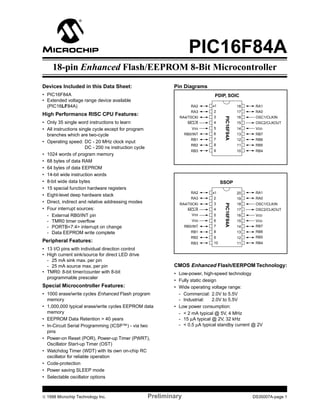
  • 1. M PIC16F84A 18-pin Enhanced Flash/EEPROM 8-Bit Microcontroller Devices Included in this Data Sheet: Pin Diagrams • PIC16F84A • Extended voltage range device available (PIC16LF84A) PDIP, SOIC RA1 17 RA0 3 16 OSC1/CLKIN MCLR 4 15 OSC2/CLKOUT VSS 5 14 VDD RB0/INT 6 13 RB7 RB1 7 12 RB6 RB2 8 11 RB5 RB3 • Only 35 single word instructions to learn • All instructions single cycle except for program branches which are two-cycle • Operating speed: DC - 20 MHz clock input DC - 200 ns instruction cycle • 1024 words of program memory • 68 bytes of data RAM • 64 bytes of data EEPROM • 14-bit wide instruction words • 8-bit wide data bytes • 15 special function hardware registers • Eight-level deep hardware stack • Direct, indirect and relative addressing modes • Four interrupt sources: - External RB0/INT pin - TMR0 timer overflow - PORTB<7:4> interrupt on change - Data EEPROM write complete 18 2 RA4/T0CKI High Performance RISC CPU Features: •1 RA3 9 10 RB4 SSOP •1 20 RA1 RA3 2 19 RA0 RA4/T0CKI 3 18 OSC1/CLKIN MCLR VSS 4 17 OSC2/CLKOUT 16 VSS 6 RB0/INT 7 14 VDD VDD RB7 RB1 8 13 RB6 RB2 9 10 12 11 RB5 RB3 • 13 I/O pins with individual direction control • High current sink/source for direct LED drive - 25 mA sink max. per pin - 25 mA source max. per pin • TMR0: 8-bit timer/counter with 8-bit programmable prescaler 5 PIC16F84A RA2 Peripheral Features: 15 RB4 CMOS Enhanced Flash/EERPOM Technology: Special Microcontroller Features: • 1000 erase/write cycles Enhanced Flash program memory • 1,000,000 typical erase/write cycles EEPROM data memory • EEPROM Data Retention > 40 years • In-Circuit Serial Programming (ICSP™) - via two pins • Power-on Reset (POR), Power-up Timer (PWRT), Oscillator Start-up Timer (OST) • Watchdog Timer (WDT) with its own on-chip RC oscillator for reliable operation • Code-protection • Power saving SLEEP mode • Selectable oscillator options © 1998 Microchip Technology Inc. PIC16F84A RA2 • Low-power, high-speed technology • Fully static design • Wide operating voltage range: - Commercial: 2.0V to 5.5V - Industrial: 2.0V to 5.5V • Low power consumption: - < 2 mA typical @ 5V, 4 MHz - 15 µA typical @ 2V, 32 kHz - < 0.5 µA typical standby current @ 2V Preliminary DS35007A-page 1
  • 2. PIC16F84A Table of Contents 1.0 Device Overview ............................................................................................................................................................................ 3 2.0 Memory Organization..................................................................................................................................................................... 5 3.0 I/O Ports....................................................................................................................................................................................... 13 4.0 Timer0 Module ............................................................................................................................................................................. 17 5.0 Data EEPROM Memory............................................................................................................................................................... 19 6.0 Special Features of the CPU ....................................................................................................................................................... 21 7.0 Instruction Set Summary.............................................................................................................................................................. 33 8.0 Development Support .................................................................................................................................................................. 35 9.0 Electrical Characteristics for PIC16F84A..................................................................................................................................... 41 10.0 DC & AC Characteristics Graphs/Tables ..................................................................................................................................... 53 11.0 Packaging Information ................................................................................................................................................................. 55 Appendix A: Revision History ........................................................................................................................................................... 59 Appendix B: Conversion Considerations.......................................................................................................................................... 59 Appendix C: Migration from Baseline to Midrange Devices ............................................................................................................. 62 Index ................................................................................................................................................................................................... 63 On-Line Support................................................................................................................................................................................... 65 Reader Response ................................................................................................................................................................................ 66 PIC16F84A Product Identification System ........................................................................................................................................... 67 To Our Valued Customers Most Current Data Sheet To obtain the most up-to-date version of this data sheet, please check our Worldwide Web site at: http://www.microchip.com You can determine the version of a data sheet by examining its literature number found on the bottom outside corner of any page. The last character of the literature number is the version number. e.g., DS30000A is version A of document DS30000. Errata An errata sheet may exist for current devices, describing minor operational differences (from the data sheet) and recommended workarounds. As device/documentation issues become known to us, we will publish an errata sheet. The errata will specify the revision of silicon and revision of document to which it applies. To determine if an errata sheet exists for a particular device, please check with one of the following: • Microchip’s Worldwide Web site; http://www.microchip.com • Your local Microchip sales office (see last page) • The Microchip Corporate Literature Center; U.S. FAX: (602) 786-7277 When contacting a sales office or the literature center, please specify which device, revision of silicon and data sheet (include literature number) you are using. Corrections to this Data Sheet We constantly strive to improve the quality of all our products and documentation. We have spent a great deal of time to ensure that this document is correct. However, we realize that we may have missed a few things. If you find any information that is missing or appears in error, please: • Fill out and mail in the reader response form in the back of this data sheet. • E-mail us at webmaster@microchip.com. We appreciate your assistance in making this a better document. DS35007A-page 2 Preliminary © 1998 Microchip Technology Inc.
  • 3. PIC16F84A 1.0 DEVICE OVERVIEW The program memory contains 1K words, which translates to 1024 instructions, since each 14-bit program memory word is the same width as each device instruction. The data memory (RAM) contains 68 bytes. Data EEPROM is 64 bytes. This document contains device-specific information for the operation of the PIC16F84A device. Additional information may be found in the PICmicro™ Mid-Range Reference Manual, (DS33023), which may be downloaded from the Microchip website. The Reference Manual should be considered a complementary document to this data sheet, and is highly recommended reading for a better understanding of the device architecture and operation of the peripheral modules. There are also 13 I/O pins that are user-configured on a pin-to-pin basis. Some pins are multiplexed with other device functions. These functions include: • External interrupt • Change on PORTB interrupt • Timer0 clock input The PIC16F84A belongs to the mid-range family of the PICmicro™ microcontroller devices. A block diagram of the device is shown in Figure 1-1. FIGURE 1-1: Table 1-1 details the pinout of the device with descriptions and details for each pin. PIC16F84A BLOCK DIAGRAM Data Bus 13 8 Program Counter EEPROM Data Memory Flash Program Memory PIC16F84A 1K x 14 Program Bus 8 Level Stack (13-bit) 14 RAM File Registers EEDATA PIC16F84A 68 x 8 7 RAM Addr EEPROM Data Memory 64 x 8 EEADR Addr Mux Instruction reg 7 Direct Addr 5 TMR0 Indirect Addr FSR reg RA4/T0CKI STATUS reg 8 MUX Power-up Timer Instruction Decode & Control Oscillator Start-up Timer 8 ALU Power-on Reset Watchdog Timer Timing Generation I/O Ports RA3:RA0 W reg RB7:RB1 RB0/INT OSC2/CLKOUT OSC1/CLKIN MCLR © 1998 Microchip Technology Inc. VDD, VSS Preliminary DS35007A-page 3
  • 4. PIC16F84A TABLE 1-1 PIC16F84A PINOUT DESCRIPTION Pin Name DIP No. SOIC No. SSOP No. I/O/P Type Buffer Type OSC1/CLKIN 16 16 18 I OSC2/CLKOUT 15 15 19 O — Oscillator crystal output. Connects to crystal or resonator in crystal oscillator mode. In RC mode, OSC2 pin outputs CLKOUT which has 1/4 the frequency of OSC1, and denotes the instruction cycle rate. MCLR 4 4 4 I/P ST Master clear (reset) input/programming voltage input. This pin is an active low reset to the device. RA0 17 17 19 I/O TTL RA1 18 18 20 I/O TTL RA2 1 1 1 I/O TTL RA3 2 2 2 I/O TTL RA4/T0CKI 3 3 3 I/O ST Description ST/CMOS (3) Oscillator crystal input/external clock source input. PORTA is a bi-directional I/O port. Can also be selected to be the clock input to the TMR0 timer/counter. Output is open drain type. PORTB is a bi-directional I/O port. PORTB can be software programmed for internal weak pull-up on all inputs. RB0/INT 6 6 7 I/O RB1 7 7 8 I/O TTL RB2 8 8 9 I/O TTL RB3 9 9 10 I/O TTL RB4 10 10 11 I/O TTL RB5 11 11 12 I/O RB0/INT can also be selected as an external interrupt pin. TTL/ST (1) TTL Interrupt on change pin. Interrupt on change pin. (2) RB6 12 12 13 I/O TTL/ST RB7 13 13 14 I/O TTL/ST (2) Interrupt on change pin. Serial programming clock. Interrupt on change pin. Serial programming data. VSS 5 5 5,6 P — Ground reference for logic and I/O pins. VDD 14 14 15,16 P — Positive supply for logic and I/O pins. Legend: I= input O = output I/O = Input/Output P = power — = Not used TTL = TTL input ST = Schmitt Trigger input Note 1: This buffer is a Schmitt Trigger input when configured as the external interrupt. 2: This buffer is a Schmitt Trigger input when used in serial programming mode. 3: This buffer is a Schmitt Trigger input when configured in RC oscillator mode and a CMOS input otherwise. DS35007A-page 4 Preliminary © 1998 Microchip Technology Inc.
  • 5. PIC16F84A MEMORY ORGANIZATION FIGURE 2-1: There are two memory blocks in the PIC16F84A. These are the program memory and the data memory. Each block has its own bus, so that access to each block can occur during the same oscillator cycle. The data memory can further be broken down into the general purpose RAM and the Special Function Registers (SFRs). The operation of the SFRs that control the “core” are described here. The SFRs used to control the peripheral modules are described in the section discussing each individual peripheral module. The data memory area also contains the data EEPROM memory. This memory is not directly mapped into the data memory, but is indirectly mapped. That is, an indirect address pointer specifies the address of the data EEPROM memory to read/write. The 64 bytes of data EEPROM memory have the address range 0h-3Fh. More details on the EEPROM memory can be found in Section 5.0. PROGRAM MEMORY MAP AND STACK - PIC16F84A PC<12:0> 13 CALL, RETURN RETFIE, RETLW Stack Level 1 • • • Stack Level 8 Reset Vector 0000h Peripheral Interrupt Vector 0004h User Memory Space 2.0 Additional information on device memory may be found in the PICmicro™ Mid-Range Reference Manual, (DS33023). 2.1 3FFh Program Memory Organization The PIC16FXX has a 13-bit program counter capable of addressing an 8K x 14 program memory space. For the PIC16F84A, the first 1K x 14 (0000h-03FFh) are physically implemented (Figure 2-1). Accessing a location above the physically implemented address will cause a wraparound. For example, for locations 20h, 420h, 820h, C20h, 1020h, 1420h, 1820h, and 1C20h will be the same instruction. 1FFFh The reset vector is at 0000h and the interrupt vector is at 0004h. © 1998 Microchip Technology Inc. Preliminary DS35007A-page 5
  • 6. PIC16F84A 2.2 Data Memory Organization 2.2.1 The data memory is partitioned into two areas. The first is the Special Function Registers (SFR) area, while the second is the General Purpose Registers (GPR) area. The SFRs control the operation of the device. Portions of data memory are banked. This is for both the SFR area and the GPR area. The GPR area is banked to allow greater than 116 bytes of general purpose RAM. The banked areas of the SFR are for the registers that control the peripheral functions. Banking requires the use of control bits for bank selection. These control bits are located in the STATUS Register. Figure 2-1 shows the data memory map organization. GENERAL PURPOSE REGISTER FILE Each General Purpose Register (GPR) is 8 bits wide and is accessed either directly or indirectly through the FSR (Section 2.4). The GPR addresses in bank 1 are mapped to addresses in bank 0. As an example, addressing location 0Ch or 8Ch will access the same GPR. FIGURE 2-1: REGISTER FILE MAP PIC16F84A File Address File Address 00h 80h TMR0 OPTION_REG 81h 02h PCL PCL 82h 03h STATUS STATUS 83h 04h FSR FSR 84h 05h PORTA TRISA 85h 06h PORTB TRISB 86h 08h EEDATA EECON1 88h 09h EEADR EECON2(1) 89h 0Ah PCLATH PCLATH 8Ah 0Bh The entire data memory can be accessed either directly using the absolute address of each register file or indirectly through the File Select Register (FSR) (Section 2.4). Indirect addressing uses the present value of the RP0 bit for access into the banked areas of data memory. Indirect addr.(1) 01h Instructions MOVWF and MOVF can move values from the W register to any location in the register file (“F”), and vice-versa. Indirect addr.(1) INTCON INTCON 8Bh 87h 07h Data memory is partitioned into two banks which contain the general purpose registers and the special function registers. Bank 0 is selected by clearing the RP0 bit (STATUS<5>). Setting the RP0 bit selects Bank 1. Each Bank extends up to 7Fh (128 bytes). The first twelve locations of each Bank are reserved for the Special Function Registers. The remainder are General Purpose Registers implemented as static RAM. 8Ch 0Ch 68 General Purpose Registers (SRAM) Mapped (accesses) in Bank 0 4Fh 50h CFh D0h FFh 7Fh Bank 0 Bank 1 Unimplemented data memory location; read as '0'. Note 1: Not a physical register. DS35007A-page 6 Preliminary © 1998 Microchip Technology Inc.
  • 7. PIC16F84A 2.2.2 The special function registers can be classified into two sets, core and peripheral. Those associated with the core functions are described in this section. Those related to the operation of the peripheral features are described in the section for that specific feature. SPECIAL FUNCTION REGISTERS The Special Function Registers (Figure 2-1 and Table 2-1) are used by the CPU and Peripheral functions to control the device operation. These registers are static RAM. TABLE 2-1 Addr REGISTER FILE SUMMARY Name Bit 7 Bit 6 Bit 5 Bit 4 Bit 3 Bit 2 Bit 1 Bit 0 Value on Power-on Reset Value on all other resets (Note3) Bank 0 00h INDF Uses contents of FSR to address data memory (not a physical register) ---- ---- ---- ---- 01h TMR0 8-bit real-time clock/counter xxxx xxxx uuuu uuuu 02h PCL Low order 8 bits of the Program Counter (PC) 0000 0000 0000 0000 0001 1xxx 000q quuu (2) 03h STATUS 04h FSR 05h PORTA (4) 06h PORTB (5) IRP RP1 TO RP0 PD Z DC C Indirect data memory address pointer 0 xxxx xxxx — — — RA4/T0CKI RA3 RA2 RA1 RA0 RB7 RB6 RB5 RB4 RB3 RB2 RB1 RB0/INT uuuu uuuu ---x xxxx ---u uuuu xxxx xxxx uuuu uuuu Unimplemented location, read as '0' 07h ---- ---- ---- ---- xxxx xxxx uuuu uuuu xxxx xxxx uuuu uuuu ---0 0000 ---0 0000 0000 000x 0000 000u ---- ---- ---- ---- 1111 1111 1111 1111 08h EEDATA EEPROM data register 09h EEADR EEPROM address register 0Ah PCLATH — — — 0Bh INTCON GIE EEIE Write buffer for upper 5 bits of the PC (1) T0IE INTE RBIE T0IF INTF RBIF Bank 1 80h INDF 81h OPTION_REG 82h PCL 83h STATUS (2) 84h FSR 85h TRISA 86h TRISB Uses contents of FSR to address data memory (not a physical register) RBPU INTEDG T0CS T0SE PSA PS2 PS1 PS0 Low order 8 bits of Program Counter (PC) IRP RP1 RP0 TO 0000 0000 Z DC C Indirect data memory address pointer 0 — — — PORTA data direction register 0000 0000 0001 1xxx 000q quuu xxxx xxxx PD uuuu uuuu ---1 1111 PORTB data direction register 1111 1111 1111 1111 Unimplemented location, read as '0' 87h ---1 1111 ---- ---- ---- ---- 88h EECON1 89h EECON2 — — — 0Ah PCLATH — — — 0Bh INTCON GIE EEIE T0IE EEIF WRERR WREN WR RD INTE RBIE T0IF INTF RBIF ---0 q000 ---- ---- ---0 0000 Write buffer for upper 5 bits of the PC (1) ---0 x000 ---- ---- EEPROM control register 2 (not a physical register) ---0 0000 0000 000x 0000 000u Legend: x = unknown, u = unchanged. - = unimplemented read as '0', q = value depends on condition. Note 1: The upper byte of the program counter is not directly accessible. PCLATH is a slave register for PC<12:8>. The contents of PCLATH can be transferred to the upper byte of the program counter, but the contents of PC<12:8> is never transferred to PCLATH. 2: The TO and PD status bits in the STATUS register are not affected by a MCLR reset. 3: Other (non power-up) resets include: external reset through MCLR and the Watchdog Timer Reset. 4: On any device reset, these pins are configured as inputs. 5: This is the value that will be in the port output latch. © 1998 Microchip Technology Inc. Preliminary DS35007A-page 7
  • 8. PIC16F84A 2.2.2.1 STATUS REGISTER The STATUS register contains the arithmetic status of the ALU, the RESET status and the bank select bit for data memory. As with any register, the STATUS register can be the destination for any instruction. If the STATUS register is the destination for an instruction that affects the Z, DC or C bits, then the write to these three bits is disabled. These bits are set or cleared according to device logic. Furthermore, the TO and PD bits are not writable. Therefore, the result of an instruction with the STATUS register as destination may be different than intended. For example, CLRF STATUS will clear the upper-three bits and set the Z bit. This leaves the STATUS register as 000u u1uu (where u = unchanged). FIGURE 2-1: R/W-0 IRP bit7 bit 7: Only the BCF, BSF, SWAPF and MOVWF instructions should be used to alter the STATUS register (Table 7-2) because these instructions do not affect any status bit. Note 1: The IRP and RP1 bits (STATUS<7:6>) are not used by the PIC16F84A and should be programmed as cleared. Use of these bits as general purpose R/W bits is NOT recommended, since this may affect upward compatibility with future products. Note 2: The C and DC bits operate as a borrow and digit borrow out bit, respectively, in subtraction. See the SUBLW and SUBWF instructions for examples. Note 3: When the STATUS register is the destination for an instruction that affects the Z, DC or C bits, then the write to these three bits is disabled. The specified bit(s) will be updated according to device logic STATUS REGISTER (ADDRESS 03h, 83h) R/W-0 RP1 R/W-0 RP0 R-1 TO R-1 PD R/W-x Z R/W-x DC R/W-x C bit0 R = Readable bit W = Writable bit U = Unimplemented bit, read as ‘0’ - n = Value at POR reset IRP: Register Bank Select bit (used for indirect addressing) The IRP bit is not used by the PIC16F84A. IRP should be maintained clear. bit 6-5: RP1:RP0: Register Bank Select bits (used for direct addressing) 00 = Bank 0 (00h - 7Fh) 01 = Bank 1 (80h - FFh) Each bank is 128 bytes. Only bit RP0 is used by the PIC16F84A. RP1 should be maintained clear. bit 4: TO: Time-out bit 1 = After power-up, CLRWDT instruction, or SLEEP instruction 0 = A WDT time-out occurred bit 3: PD: Power-down bit 1 = After power-up or by the CLRWDT instruction 0 = By execution of the SLEEP instruction bit 2: Z: Zero bit 1 = The result of an arithmetic or logic operation is zero 0 = The result of an arithmetic or logic operation is not zero bit 1: DC: Digit carry/borrow bit (for ADDWF and ADDLW instructions) (For borrow the polarity is reversed) 1 = A carry-out from the 4th low order bit of the result occurred 0 = No carry-out from the 4th low order bit of the result bit 0: C: Carry/borrow bit (for ADDWF and ADDLW instructions) 1 = A carry-out from the most significant bit of the result occurred 0 = No carry-out from the most significant bit of the result occurred Note:For borrow the polarity is reversed. A subtraction is executed by adding the two’s complement of the second operand. For rotate (RRF, RLF) instructions, this bit is loaded with either the high or low order bit of the source register. DS35007A-page 8 Preliminary © 1998 Microchip Technology Inc.
  • 9. PIC16F84A 2.2.2.2 OPTION_REG REGISTER The OPTION_REG register is a readable and writable register which contains various control bits to configure the TMR0/WDT prescaler, the external INT interrupt, TMR0, and the weak pull-ups on PORTB. FIGURE 2-1: R/W-1 RBPU bit7 Note: When the prescaler is assigned to the WDT (PSA = '1'), TMR0 has a 1:1 prescaler assignment. OPTION_REG REGISTER (ADDRESS 81h) R/W-1 INTEDG R/W-1 T0CS R/W-1 T0SE R/W-1 PSA R/W-1 PS2 R/W-1 PS1 R/W-1 PS0 bit0 bit 7: RBPU: PORTB Pull-up Enable bit 1 = PORTB pull-ups are disabled 0 = PORTB pull-ups are enabled (by individual port latch values) bit 6: INTEDG: Interrupt Edge Select bit 1 = Interrupt on rising edge of RB0/INT pin 0 = Interrupt on falling edge of RB0/INT pin bit 5: T0CS: TMR0 Clock Source Select bit 1 = Transition on RA4/T0CKI pin 0 = Internal instruction cycle clock (CLKOUT) bit 4: T0SE: TMR0 Source Edge Select bit 1 = Increment on high-to-low transition on RA4/T0CKI pin 0 = Increment on low-to-high transition on RA4/T0CKI pin bit 3: R = Readable bit W = Writable bit U = Unimplemented bit, read as ‘0’ - n = Value at POR reset PSA: Prescaler Assignment bit 1 = Prescaler assigned to the WDT 0 = Prescaler assigned to TMR0 bit 2-0: PS2:PS0: Prescaler Rate Select bits Bit Value TMR0 Rate WDT Rate 000 001 010 011 100 101 110 111 1:2 1:4 1:8 1 : 16 1 : 32 1 : 64 1 : 128 1 : 256 1:1 1:2 1:4 1:8 1 : 16 1 : 32 1 : 64 1 : 128 © 1998 Microchip Technology Inc. Preliminary DS35007A-page 9
  • 10. PIC16F84A 2.2.2.3 INTCON REGISTER The INTCON register is a readable and writable register which contains the various enable bits for all interrupt sources. FIGURE 2-1: R/W-0 GIE bit7 bit 7: Note: Interrupt flag bits get set when an interrupt condition occurs regardless of the state of its corresponding enable bit or the global enable bit, GIE (INTCON<7>). INTCON REGISTER (ADDRESS 0Bh, 8Bh) R/W-0 EEIE R/W-0 T0IE R/W-0 INTE R/W-0 RBIE R/W-0 T0IF R/W-0 INTF R/W-x RBIF bit0 R = Readable bit W = Writable bit U = Unimplemented bit, read as ‘0’ - n = Value at POR reset GIE: Global Interrupt Enable bit 1 = Enables all un-masked interrupts 0 = Disables all interrupts Note: For the operation of the interrupt structure, please refer to Section •. bit 6: EEIE: EE Write Complete Interrupt Enable bit 1 = Enables the EE write complete interrupt 0 = Disables the EE write complete interrupt bit 5: T0IE: TMR0 Overflow Interrupt Enable bit 1 = Enables the TMR0 interrupt 0 = Disables the TMR0 interrupt bit 4: INTE: RB0/INT Interrupt Enable bit 1 = Enables the RB0/INT interrupt 0 = Disables the RB0/INT interrupt bit 3: RBIE: RB Port Change Interrupt Enable bit 1 = Enables the RB port change interrupt 0 = Disables the RB port change interrupt bit 2: T0IF: TMR0 Overflow Interrupt Flag bit 1 = TMR0 has overflowed (must be cleared in software) 0 = TMR0 did not overflow bit 1: INTF: RB0/INT Interrupt Flag bit 1 = The RB0/INT interrupt occurred 0 = The RB0/INT interrupt did not occur bit 0: RBIF: RB Port Change Interrupt Flag bit 1 = When at least one of the RB7:RB4 pins changed state (must be cleared in software) 0 = None of the RB7:RB4 pins have changed state DS35007A-page 10 Preliminary © 1998 Microchip Technology Inc.
  • 11. PIC16F84A 2.3 PCL and PCLATH 2.4 The program counter (PC) specifies the address of the instruction to fetch for execution. The PC is 13 bits wide. The low byte is called the PCL register. This register is readable and writable. The high byte is called the PCH register. This register contains the PC<12:8> bits and is not directly readable or writable. All updates to the PCH register go through the PCLATH register. 2.3.1 STACK The stack allows a combination of up to 8 program calls and interrupts to occur. The stack contains the return address from this branch in program execution. Midrange devices have an 8 level deep x 13-bit wide hardware stack. The stack space is not part of either program or data space and the stack pointer is not readable or writable. The PC is PUSHed onto the stack when a CALL instruction is executed or an interrupt causes a branch. The stack is POPed in the event of a RETURN, RETLW or a RETFIE instruction execution. PCLATH is not modified when the stack is PUSHed or POPed. After the stack has been PUSHed eight times, the ninth push overwrites the value that was stored from the first push. The tenth push overwrites the second push (and so on). Indirect Addressing; INDF and FSR Registers The INDF register is not a physical register. Addressing INDF actually addresses the register whose address is contained in the FSR register (FSR is a pointer). This is indirect addressing. EXAMPLE 2-1: INDIRECT ADDRESSING • • • • Register file 05 contains the value 10h Register file 06 contains the value 0Ah Load the value 05 into the FSR register A read of the INDF register will return the value of 10h • Increment the value of the FSR register by one (FSR = 06) • A read of the INDF register now will return the value of 0Ah. Reading INDF itself indirectly (FSR = 0) will produce 00h. Writing to the INDF register indirectly results in a no-operation (although STATUS bits may be affected). A simple program to clear RAM locations 20h-2Fh using indirect addressing is shown in Example 2-2. EXAMPLE 2-2: NEXT movlw movwf clrf incf btfss goto HOW TO CLEAR RAM USING INDIRECT ADDRESSING 0x20 FSR INDF FSR FSR,4 NEXT ;initialize pointer ; to RAM ;clear INDF register ;inc pointer ;all done? ;NO, clear next CONTINUE : ;YES, continue An effective 9-bit address is obtained by concatenating the 8-bit FSR register and the IRP bit (STATUS<7>), as shown in Figure 2-1. However, IRP is not used in the PIC16F84A. © 1998 Microchip Technology Inc. Preliminary DS35007A-page 11
  • 12. PIC16F84A FIGURE 2-1: DIRECT/INDIRECT ADDRESSING Indirect Addressing Direct Addressing RP1 RP0 6 0 from opcode IRP (2) bank select 7 (FSR) 0 (2) location select bank select 00 location select 01 00h 80h 0Bh 0Ch Addresses map back to Bank 0 Data Memory (1) 4Fh 50h (3) (3) 7Fh FFh Bank 0 Bank 1 Note 1: For memory map detail see Figure 2-1. 2: Maintain as clear for upward compatiblity with future products. 3: Not implemented. DS35007A-page 12 Preliminary © 1998 Microchip Technology Inc.
  • 13. PIC16F84A 3.0 I/O PORTS FIGURE 3-1: Some pins for these I/O ports are multiplexed with an alternate function for the peripheral features on the device. In general, when a peripheral is enabled, that pin may not be used as a general purpose I/O pin. Additional information on I/O ports may be found in the PICmicro™ Mid-Range Reference Manual, (DS33023). BLOCK DIAGRAM OF PINS RA3:RA0 Data bus D WR Port Q VDD CK Q P Data Latch 3.1 PORTA and TRISA Registers N PORTA is a 5-bit wide bi-directional port. The corresponding data direction register is TRISA. Setting a TRISA bit (=1) will make the corresponding PORTA pin an input, i.e., put the corresponding output driver in a hi-impedance mode. Clearing a TRISA bit (=0) will make the corresponding PORTA pin an output, i.e., put the contents of the output latch on the selected pin. Note: D WR TRIS Reading the PORTA register reads the status of the pins whereas writing to it will write to the port latch. All write operations are read-modify-write operations. Therefore a write to a port implies that the port pins are read, this value is modified, and then written to the port data latch. Pin RA4 is multiplexed with the Timer0 module clock input to become the RA4/T0CKI pin. The RA4/T0CKI pin is a Schmitt Trigger input and an open drain output. All other RA port pins have TTL input levels and full CMOS output drivers. EXAMPLE 3-1: VSS CK Q TRIS Latch On a Power-on Reset, these pins are configured as inputs and read as '0'. I/O pin Q TTL input buffer RD TRIS Q D EN RD PORT Note: I/O pins have protection diodes to VDD and VSS. INITIALIZING PORTA BCF CLRF STATUS, RP0 PORTA BSF MOVLW STATUS, RP0 0x0F MOVWF TRISA ; ; ; ; ; ; ; ; ; ; ; ; Initialize PORTA by clearing output data latches Select Bank 1 Value used to initialize data direction Set RA<3:0> as inputs RA4 as output TRISA<7:5> are always read as '0'. © 1998 Microchip Technology Inc. Preliminary DS35007A-page 13
  • 14. PIC16F84A FIGURE 3-2: BLOCK DIAGRAM OF PIN RA4 Data bus D Q CK WR PORT Q RA4 pin N Data Latch VSS D CK WR TRIS Q Q Schmitt Trigger input buffer TRIS Latch RD TRIS Q D EN EN RD PORT TMR0 clock input Note: I/O pin has protection diodes to VSS only. TABLE 3-1 PORTA FUNCTIONS Name Bit0 Buffer Type RA0 RA1 RA2 RA3 RA4/T0CKI bit0 bit1 bit2 bit3 bit4 TTL TTL TTL TTL ST Function Input/output Input/output Input/output Input/output Input/output or external clock input for TMR0. Output is open drain type. Legend: TTL = TTL input, ST = Schmitt Trigger input TABLE 3-2 SUMMARY OF REGISTERS ASSOCIATED WITH PORTA Address Name Bit 7 Bit 6 Bit 5 Bit 4 Bit 3 Bit 2 05h PORTA — — — RA4/T0CKI RA3 RA2 85h TRISA — — — TRISA4 TRISA3 TRISA2 Bit 0 Value on Power-on Reset Value on all other resets RA1 RA0 ---x xxxx ---u uuuu TRISA1 TRISA0 ---1 1111 ---1 1111 Bit 1 Legend: x = unknown, u = unchanged, - = unimplemented read as '0'. Shaded cells are unimplemented, read as '0' DS35007A-page 14 Preliminary © 1998 Microchip Technology Inc.
  • 15. PIC16F84A 3.2 PORTB and TRISB Registers PORTB is an 8-bit wide bi-directional port. The corresponding data direction register is TRISB. Setting a TRISB bit (=1) will make the corresponding PORTB pin an input, i.e., put the corresponding output driver in a hi-impedance mode. Clearing a TRISB bit (=0) will make the corresponding PORTB pin an output, i.e., put the contents of the output latch on the selected pin. EXAMPLE 3-1: BCF CLRF BSF MOVLW MOVWF INITIALIZING PORTB STATUS, RP0 PORTB ; ; ; ; ; ; ; ; ; ; ; STATUS, RP0 0xCF TRISB Initialize PORTB by clearing output data latches Select Bank 1 Value used to initialize data direction Set RB<3:0> as inputs RB<5:4> as outputs RB<7:6> as inputs Each of the PORTB pins has a weak internal pull-up. A single control bit can turn on all the pull-ups. This is performed by clearing bit RBPU (OPTION<7>). The weak pull-up is automatically turned off when the port pin is configured as an output. The pull-ups are disabled on a Power-on Reset. FIGURE 3-3: Four of PORTB’s pins, RB7:RB4, have an interrupt on change feature. Only pins configured as inputs can cause this interrupt to occur (i.e. any RB7:RB4 pin configured as an output is excluded from the interrupt on change comparison). The input pins (of RB7:RB4) are compared with the old value latched on the last read of PORTB. The “mismatch” outputs of RB7:RB4 are OR’ed together to generate the RB Port Change Interrupt with flag bit RBIF (INTCON<0>). This interrupt can wake the device from SLEEP. The user, in the interrupt service routine, can clear the interrupt in the following manner: a) b) Any read or write of PORTB. This will end the mismatch condition. Clear flag bit RBIF. A mismatch condition will continue to set flag bit RBIF. Reading PORTB will end the mismatch condition, and allow flag bit RBIF to be cleared. The interrupt on change feature is recommended for wake-up on key depression operation and operations where PORTB is only used for the interrupt on change feature. Polling of PORTB is not recommended while using the interrupt on change feature. FIGURE 3-4: BLOCK DIAGRAM OF PINS RB3:RB0 VDD BLOCK DIAGRAM OF PINS RB7:RB4 RBPU(1) Data bus weak P pull-up Data Latch D Q VDD RBPU(1) Data bus weak P pull-up WR Port TRIS Latch D Q Data Latch D WR Port Q I/O pin(2) CK I/O pin(2) CK WR TRIS TTL Input Buffer CK TRIS Latch D WR TRIS Q RD TRIS TTL Input Buffer CK Q RD Port Latch RD TRIS Q RD Port D EN RB0/INT D Schmitt Trigger Buffer EN RD Port Note 1: TRISB = '1' enables weak pull-up (if RBPU = '0' in the OPTION_REG register). Set RBIF 2: I/O pins have diode protection to VDD and VSS. From other RB7:RB4 pins Q D EN RD Port Note 1: TRISB = '1' enables weak pull-up (if RBPU = '0' in the OPTION_REG register). 2: I/O pins have diode protection to VDD and VSS. © 1998 Microchip Technology Inc. Preliminary DS35007A-page 15
  • 16. PIC16F84A TABLE 3-3 PORTB FUNCTIONS Name Bit Buffer Type I/O Consistency Function TTL/ST(1) Input/output pin or external interrupt input. Internal software programmable weak pull-up. RB1 bit1 TTL Input/output pin. Internal software programmable weak pull-up. RB2 bit2 TTL Input/output pin. Internal software programmable weak pull-up. RB3 bit3 TTL Input/output pin. Internal software programmable weak pull-up. RB4 bit4 TTL Input/output pin (with interrupt on change). Internal software programmable weak pull-up. RB5 bit5 TTL Input/output pin (with interrupt on change). Internal software programmable weak pull-up. RB6 bit6 TTL/ST(2) Input/output pin (with interrupt on change). Internal software programmable weak pull-up. Serial programming clock. RB7 bit7 TTL/ST(2) Input/output pin (with interrupt on change). Internal software programmable weak pull-up. Serial programming data. Legend: TTL = TTL input, ST = Schmitt Trigger. Note 1: This buffer is a Schmitt Trigger input when configured as the external interrupt. 2: This buffer is a Schmitt Trigger input when used in serial programming mode. RB0/INT bit0 TABLE 3-4 Addr SUMMARY OF REGISTERS ASSOCIATED WITH PORTB Name Bit 7 Bit 6 Bit 5 Bit 4 Bit 3 Bit 2 Bit 1 Bit 0 Value on Power-on Reset Value on all other resets 06h PORTB RB7 RB6 RB5 RB4 RB3 RB2 RB1 RB0/INT xxxx xxxx uuuu uuuu 86h TRISB TRISB7 TRISB6 TRISB5 TRISB4 TRISB3 TRISB2 TRISB1 TRISB0 1111 1111 1111 1111 81h OPTION_REG RBPU INTEDG T0CS T0SE PSA PS2 PS1 PS0 1111 1111 1111 1111 Legend: x = unknown, u = unchanged. Shaded cells are not used by PORTB. DS35007A-page 16 Preliminary © 1998 Microchip Technology Inc.
  • 17. PIC16F84A 4.0 TIMER0 MODULE Additional information on external clock requirements is available in the PICmicro™ Mid-Range Reference Manual, (DS33023). The Timer0 module timer/counter has the following features: • • • • • • 4.2 8-bit timer/counter Readable and writable Internal or external clock select Edge select for external clock 8-bit software programmable prescaler Interrupt on overflow from FFh to 00h An 8-bit counter is available as a prescaler for the Timer0 module, or as a postscaler for the Watchdog Timer, respectively (Figure 4-2). For simplicity, this counter is being referred to as “prescaler” throughout this data sheet. Note that there is only one prescaler available which is mutually exclusively shared between the Timer0 module and the Watchdog Timer. Thus, a prescaler assignment for the Timer0 module means that there is no prescaler for the Watchdog Timer, and vice-versa. Figure 4-1 is a simplified block diagram of the Timer0 module. Additional information on timer modules is available in the PICmicro™ Mid-Range Reference Manual, (DS33023). 4.1 The prescaler is not readable or writable. The PSA and PS2:PS0 bits (OPTION_REG<3:0>) determine the prescaler assignment and prescale ratio. Timer0 Operation Timer0 can operate as a timer or as a counter. Clearing bit PSA will assign the prescaler to the Timer0 module. When the prescaler is assigned to the Timer0 module, prescale values of 1:2, 1:4, ..., 1:256 are selectable. Timer mode is selected by clearing bit T0CS (OPTION_REG<5>). In timer mode, the Timer0 module will increment every instruction cycle (without prescaler). If the TMR0 register is written, the increment is inhibited for the following two instruction cycles. The user can work around this by writing an adjusted value to the TMR0 register. Setting bit PSA will assign the prescaler to the Watchdog Timer (WDT). When the prescaler is assigned to the WDT, prescale values of 1:1, 1:2, ..., 1:128 are selectable. Counter mode is selected by setting bit T0CS (OPTION_REG<5>). In counter mode, Timer0 will increment either on every rising or falling edge of pin RA4/T0CKI. The incrementing edge is determined by the Timer0 Source Edge Select bit T0SE (OPTION_REG<4>). Clearing bit T0SE selects the rising edge. Restrictions on the external clock input are discussed below. When assigned to the Timer0 module, all instructions writing to the TMR0 register (e.g. CLRF 1, MOVWF 1, BSF 1,x....etc.) will clear the prescaler. When assigned to WDT, a CLRWDT instruction will clear the prescaler along with the WDT. Note: When an external clock input is used for Timer0, it must meet certain requirements. The requirements ensure the external clock can be synchronized with the internal phase clock (TOSC). Also, there is a delay in the actual incrementing of Timer0 after synchronization. FIGURE 4-1: Prescaler Writing to TMR0 when the prescaler is assigned to Timer0 will clear the prescaler count, but will not change the prescaler assignment. TIMER0 BLOCK DIAGRAM Data bus FOSC/4 0 PSout 1 1 Programmable Prescaler RA4/T0CKI pin 0 8 Sync with Internal clocks TMR0 PSout (2 cycle delay) T0SE 3 PS2, PS1, PS0 PSA T0CS Set interrupt flag bit T0IF on overflow Note 1: T0CS, T0SE, PSA, PS2:PS0 (OPTION_REG<5:0>). 2: The prescaler is shared with Watchdog Timer (refer to Figure 4-2 for detailed block diagram). © 1998 Microchip Technology Inc. Preliminary DS35007A-page 17
  • 18. PIC16F84A 4.2.1 4.3 SWITCHING PRESCALER ASSIGNMENT The prescaler assignment is fully under software control, i.e., it can be changed “on the fly” during program execution. Note: The TMR0 interrupt is generated when the TMR0 register overflows from FFh to 00h. This overflow sets bit T0IF (INTCON<2>). The interrupt can be masked by clearing bit T0IE (INTCON<5>). Bit T0IF must be cleared in software by the Timer0 module interrupt service routine before re-enabling this interrupt. The TMR0 interrupt cannot awaken the processor from SLEEP since the timer is shut off during SLEEP. To avoid an unintended device RESET, a specific instruction sequence (shown in the PICmicro™ Mid-Range Reference Manual, DS3023) must be executed when changing the prescaler assignment from Timer0 to the WDT. This sequence must be followed even if the WDT is disabled. FIGURE 4-2: Timer0 Interrupt BLOCK DIAGRAM OF THE TIMER0/WDT PRESCALER Data Bus CLKOUT (=Fosc/4) 0 RA4/T0CKI pin 8 M U X 1 M U X 0 1 SYNC 2 Cycles TMR0 reg T0SE T0CS 0 1 Watchdog Timer Set flag bit T0IF on Overflow PSA 8-bit Prescaler M U X 8 8 - to - 1MUX PS2:PS0 PSA 1 0 WDT Enable bit MUX PSA WDT Time-out Note: T0CS, T0SE, PSA, PS2:PS0 are (OPTION_REG<5:0>). TABLE 4-1 REGISTERS ASSOCIATED WITH TIMER0 Address Name 01h TMR0 0Bh,8Bh INTCON 81h OPTION_REG 85h TRISA Bit 7 Bit 6 Bit 5 Bit 3 Bit 2 Bit 1 Bit 0 Timer0 module’s register GIE PEIE RBPU INTEDG — — T0IE INTE RBIE T0IF INTF RBIF T0CS T0SE PSA PS2 PS1 PS0 PORTA Data Direction Register Value on POR, BOR Value on all other resets xxxx xxxx Bit 4 uuuu uuuu 0000 000x 0000 000u 1111 1111 1111 1111 --11 1111 --11 1111 Legend: x = unknown, u = unchanged, - = unimplemented locations read as '0'. Shaded cells are not used by Timer0. DS35007A-page 18 Preliminary © 1998 Microchip Technology Inc.
  • 19. PIC16F84A 5.0 DATA EEPROM MEMORY The EEPROM data memory is readable and writable during normal operation (full VDD range). This memory is not directly mapped in the register file space. Instead it is indirectly addressed through the Special Function Registers. There are four SFRs used to read and write this memory. These registers are: The EEPROM data memory allows byte read and write. A byte write automatically erases the location and writes the new data (erase before write). The EEPROM data memory is rated for high erase/write cycles. The write time is controlled by an on-chip timer. The writetime will vary with voltage and temperature as well as from chip to chip. Please refer to AC specifications for exact limits. • • • • EECON1 EECON2 (Not a physically implemented register) EEDATA EEADR When the device is code protected, the CPU may continue to read and write the data EEPROM memory. The device programmer can no longer access this memory. EEDATA holds the 8-bit data for read/write, and EEADR holds the address of the EEPROM location being accessed. PIC16F84A devices have 64 bytes of data EEPROM with an address range from 0h to 3Fh. Additional information on the Data EEPROM is available in the PICmicro™ Mid-Range Reference Manual, (DS33023). FIGURE 5-1: EECON1 REGISTER (ADDRESS 88h) U U U R/W-0 R/W-x R/W-0 R/S-0 R/S-x — — — EEIF WRERR WREN WR RD bit7 bit0 R W S U = Readable bit = Writable bit = Settable bit = Unimplemented bit, read as ‘0’ - n = Value at POR reset bit 7:5 Unimplemented: Read as '0' bit 4 EEIF: EEPROM Write Operation Interrupt Flag bit 1 = The write operation completed (must be cleared in software) 0 = The write operation is not complete or has not been started bit 3 WRERR: EEPROM Error Flag bit 1 = A write operation is prematurely terminated (any MCLR reset or any WDT reset during normal operation) 0 = The write operation completed bit 2 WREN: EEPROM Write Enable bit 1 = Allows write cycles 0 = Inhibits write to the data EEPROM bit 1 WR: Write Control bit 1 = initiates a write cycle. (The bit is cleared by hardware once write is complete. The WR bit can only be set (not cleared) in software. 0 = Write cycle to the data EEPROM is complete bit 0 RD: Read Control bit 1 = Initiates an EEPROM read (read takes one cycle. RD is cleared in hardware. The RD bit can only be set (not cleared) in software). 0 = Does not initiate an EEPROM read © 1998 Microchip Technology Inc. Preliminary DS35007A-page 19
  • 20. PIC16F84A 5.1 Reading the EEPROM Data Memory code execution (i.e., lost programs). The user should keep the WREN bit clear at all times, except when updating EEPROM. The WREN bit is not cleared by hardware To read a data memory location, the user must write the address to the EEADR register and then set control bit RD (EECON1<0>). The data is available, in the very next cycle, in the EEDATA register; therefore it can be read in the next instruction. EEDATA will hold this value until another read or until it is written to by the user (during a write operation). EXAMPLE 5-1: BCF MOVLW MOVWF BSF BSF BCF MOVF 5.2 After a write sequence has been initiated, clearing the WREN bit will not affect this write cycle. The WR bit will be inhibited from being set unless the WREN bit is set. At the completion of the write cycle, the WR bit is cleared in hardware and the EE Write Complete Interrupt Flag bit (EEIF) is set. The user can either enable this interrupt or poll this bit. EEIF must be cleared by software. DATA EEPROM READ STATUS, RP0 CONFIG_ADDR EEADR STATUS, RP0 EECON1, RD STATUS, RP0 EEDATA, W ; ; ; ; ; ; ; Bank 0 Address to read Bank 1 EE Read Bank 0 W = EEDATA 5.3 Depending on the application, good programming practice may dictate that the value written to the Data EEPROM should be verified (Example 5-1) to the desired value to be written. This should be used in applications where an EEPROM bit will be stressed near the specification limit. The Total Endurance disk will help determine your comfort level. Writing to the EEPROM Data Memory To write an EEPROM data location, the user must first write the address to the EEADR register and the data to the EEDATA register. Then the user must follow a specific sequence to initiate the write for each byte. Required Sequence EXAMPLE 5-1: Generally the EEPROM write failure will be a bit which was written as a '0', but reads back as a '1' (due to leakage off the bit). DATA EEPROM WRITE BSF BCF BSF MOVLW MOVWF MOVLW MOVWF BSF STATUS, RP0 INTCON, GIE EECON1, WREN 55h EECON2 AAh EECON2 EECON1,WR BSF INTCON, GIE ; ; ; ; ; ; ; ; ; ; EXAMPLE 5-1: Bank 1 Disable INTs. Enable Write BCF : : MOVF BSF Write 55h Write AAh Set WR bit begin write Enable INTs. BSF STATUS, RP0 ; ; ; EEDATA, W ; STATUS, RP0 ; Bank 0 Any code can go here Must be in Bank 0 Bank 1 EECON1, RD ; YES, Read the ; value written STATUS, RP0 ; Bank 0 BCF ; ; Is the value written (in W reg) and ; read (in EEDATA) the same? ; SUBWF EEDATA, W ; BTFSS STATUS, Z ; Is difference 0? GOTO WRITE_ERR ; NO, Write error : ; YES, Good write : ; Continue program Additionally, the WREN bit in EECON1 must be set to enable write. This mechanism prevents accidental writes to data EEPROM due to errant (unexpected) Address WRITE VERIFY READ The write will not initiate if the above sequence is not exactly followed (write 55h to EECON2, write AAh to EECON2, then set WR bit) for each byte. We strongly recommend that interrupts be disabled during this code segment. TABLE 5-1 Write Verify REGISTERS/BITS ASSOCIATED WITH DATA EEPROM Name Bit 7 Bit 6 08h EEDATA EEADR EECON1 89h EECON2 Bit 0 — — — EEIF WRERR WREN EEPROM control register 2 WR RD uuuu uuuu uuuu uuuu ---0 x000 ---0 q000 ---- ---- Bit 1 Value on all other resets xxxx xxxx Bit 2 EEPROM address register 88h Bit 3 EEPROM data register 09h Bit 4 Value on Power-on Reset xxxx xxxx Bit 5 ---- ---- Legend: x = unknown, u = unchanged, - = unimplemented read as '0', q = value depends upon condition. Shaded cells are not used by data EEPROM. DS35007A-page 20 Preliminary © 1998 Microchip Technology Inc.
  • 21. PIC16F84A 6.0 SPECIAL FEATURES OF THE CPU What sets a microcontroller apart from other processors are special circuits to deal with the needs of real time applications. The PIC16F84A has a host of such features intended to maximize system reliability, minimize cost through elimination of external components, provide power saving operating modes and offer code protection. These features are: • OSC Selection • Reset - Power-on Reset (POR) - Power-up Timer (PWRT) - Oscillator Start-up Timer (OST) • Interrupts • Watchdog Timer (WDT) • SLEEP • Code protection • ID locations • In-circuit serial programming SLEEP mode offers a very low current power-down mode. The user can wake-up from SLEEP through external reset, Watchdog Timer time-out or through an interrupt. Several oscillator options are provided to allow the part to fit the application. The RC oscillator option saves system cost while the LP crystal option saves power. A set of configuration bits are used to select the various options. Additional information on special features is available in the PICmicro™ Mid-Range Reference Manual, (DS33023). 6.1 The PIC16F84A has a Watchdog Timer which can be shut off only through configuration bits. It runs off its own RC oscillator for added reliability. There are two timers that offer necessary delays on power-up. One is the Oscillator Start-up Timer (OST), intended to keep FIGURE 6-1: the chip in reset until the crystal oscillator is stable. The other is the Power-up Timer (PWRT), which provides a fixed delay of 72 ms (nominal) on power-up only. This design keeps the device in reset while the power supply stabilizes. With these two timers on-chip, most applications need no external reset circuitry. Configuration Bits The configuration bits can be programmed (read as '0') or left unprogrammed (read as '1') to select various device configurations. These bits are mapped in program memory location 2007h. Address 2007h is beyond the user program memory space and it belongs to the special test/configuration memory space (2000h - 3FFFh). This space can only be accessed during programming. CONFIGURATION WORD - PIC16F84A R/P-u R/P-u R/P-u R/P-u R/P-u R/P-u R/P-u R/P-u R/P-u CP CP CP CP CP CP CP CP CP bit13 R/P-u CP R/P-u R/P-u R/P-u R/P-u PWRTE WDTE FOSC1 FOSC0 bit0 R = Readable bit P = Programmable bit - n = Value at POR reset u = unchanged bit 13:4 CP: Code Protection bit 1 = Code protection off 0 = All memory is code protected bit 3 PWRTE: Power-up Timer Enable bit 1 = Power-up timer is disabled 0 = Power-up timer is enabled bit 2 WDTE: Watchdog Timer Enable bit 1 = WDT enabled 0 = WDT disabled bit 1:0 FOSC1:FOSC0: Oscillator Selection bits 11 = RC oscillator 10 = HS oscillator 01 = XT oscillator 00 = LP oscillator © 1998 Microchip Technology Inc. Preliminary DS35007A-page 21
  • 22. PIC16F84A 6.2 Oscillator Configurations 6.2.1 OSCILLATOR TYPES TABLE 6-1 The PIC16F84A can be operated in four different oscillator modes. The user can program two configuration bits (FOSC1 and FOSC0) to select one of these four modes: • • • • LP XT HS RC Low Power Crystal Crystal/Resonator High Speed Crystal/Resonator Resistor/Capacitor 6.2.2 CAPACITOR SELECTION FOR CERAMIC RESONATORS Ranges Tested: Mode Freq XT 455 kHz 2.0 MHz 4.0 MHz 8.0 MHz 10.0 MHz HS Note : CRYSTAL OSCILLATOR / CERAMIC RESONATORS In XT, LP or HS modes a crystal or ceramic resonator is connected to the OSC1/CLKIN and OSC2/CLKOUT pins to establish oscillation (Figure 6-2). OSC1/C1 OSC2/C2 47 - 100 pF 47 - 100 pF 15 - 33 pF 15 - 33 pF 15 - 33 pF 15 - 33 pF 15 - 33 pF 15 - 33 pF 15 - 33 pF 15 - 33 pF Recommended values of C1 and C2 are identical to the ranges tested table. Higher capacitance increases the stability of the oscillator but also increases the start-up time. These values are for design guidance only. Since each resonator has its own characteristics, the user should consult the resonator manufacturer for the appropriate values of external components. Resonators Tested: FIGURE 6-2: CRYSTAL/CERAMIC RESONATOR OPERATION (HS, XT OR LP OSC CONFIGURATION) C1(1) 455 kHz 2.0 MHz 4.0 MHz 8.0 MHz 10.0 MHz OSC1 XTAL To internal logic RF(3) OSC2 Panasonic EFO-A455K04B Murata Erie CSA2.00MG Murata Erie CSA4.00MG Murata Erie CSA8.00MT Murata Erie CSA10.00MTZ ± 0.3% ± 0.5% ± 0.5% ± 0.5% ± 0.5% None of the resonators had built-in capacitors. TABLE 6-2 CAPACITOR SELECTION FOR CRYSTAL OSCILLATOR SLEEP RS(2) Note1: 2: 3: PIC16FXX See Table 6-1 for recommended values of C1 and C2. A series resistor (RS) may be required for AT strip cut crystals. RF varies with the crystal chosen. The PIC16F84A oscillator design requires the use of a parallel cut crystal. Use of a series cut crystal may give a frequency out of the crystal manufacturers specifications. When in XT, LP or HS modes, the device can have an external clock source to drive the OSC1/CLKIN pin (Figure 6-3). FIGURE 6-3: EXTERNAL CLOCK INPUT OPERATION (HS, XT OR LP OSC CONFIGURATION) OSC1 Clock from ext. system PIC16FXX Open DS35007A-page 22 OSC2 Mode Freq OSC1/C1 OSC2/C2 LP C2(1) 32 kHz 200 kHz 100 kHz 2 MHz 4 MHz 4 MHz 10 MHz 68 - 100 pF 15 - 33 pF 100 - 150 pF 15 - 33 pF 15 - 33 pF 15 - 33 pF 15 - 33 pF 68 - 100 pF 15 - 33 pF 100 - 150 pF 15 - 33 pF 15 - 33 pF 15 - 33 pF 15 - 33 pF XT HS Note : Higher capacitance increases the stability of oscillator but also increases the start-up time. These values are for design guidance only. Rs may be required in HS mode as well as XT mode to avoid overdriving crystals with low drive level specification. Since each crystal has its own characteristics, the user should consult the crystal manufacturer for appropriate values of external components. For VDD > 4.5V, C1 = C2 ≈ 30 pF is recommended. Crystals Tested: 32.768 kHz 100 kHz 200 kHz 1.0 MHz 2.0 MHz 4.0 MHz 10.0 MHz Preliminary Epson C-001R32.768K-A Epson C-2 100.00 KC-P STD XTL 200.000 KHz ECS ECS-10-13-2 ECS ECS-20-S-2 ECS ECS-40-S-4 ECS ECS-100-S-4 ± 20 PPM ± 20 PPM ± 20 PPM ± 50 PPM ± 50 PPM ± 50 PPM ± 50 PPM © 1998 Microchip Technology Inc.
  • 23. PIC16F84A 6.2.3 6.3 RC OSCILLATOR For timing insensitive applications the RC device option offers additional cost savings. The RC oscillator frequency is a function of the supply voltage, the resistor (Rext) values, capacitor (Cext) values, and the operating temperature. In addition to this, the oscillator frequency will vary from unit to unit due to normal process parameter variation. Furthermore, the difference in lead frame capacitance between package types also affects the oscillation frequency, especially for low Cext values. The user needs to take into account variation due to tolerance of the external R and C components. Figure 6-4 shows how an R/C combination is connected to the PIC16F84A. FIGURE 6-4: RC OSCILLATOR MODE VDD Rext Internal clock OSC1 Cext PIC16FXX VSS OSC2/CLKOUT Fosc/4 Recommended values: 5 kΩ ≤ Rext ≤ 100 kΩ Cext > 20pF Reset The PIC16F84A differentiates between various kinds of reset: • • • • • Power-on Reset (POR) MCLR reset during normal operation MCLR reset during SLEEP WDT Reset (during normal operation) WDT Wake-up (during SLEEP) Figure 6-5 shows a simplified block diagram of the on-chip reset circuit. The MCLR reset path has a noise filter to ignore small pulses. The electrical specifications state the pulse width requirements for the MCLR pin. Some registers are not affected in any reset condition; their status is unknown on a POR reset and unchanged in any other reset. Most other registers are reset to a “reset state” on POR, MCLR or WDT reset during normal operation and on MCLR reset during SLEEP. They are not affected by a WDT reset during SLEEP, since this reset is viewed as the resumption of normal operation. Table 6-3 gives a description of reset conditions for the program counter (PC) and the STATUS register. Table 6-4 gives a full description of reset states for all registers. The TO and PD bits are set or cleared differently in different reset situations (Section 6.7). These bits are used in software to determine the nature of the reset. FIGURE 6-5: SIMPLIFIED BLOCK DIAGRAM OF ON-CHIP RESET CIRCUIT External Reset MCLR WDT Module SLEEP WDT Time_Out Reset VDD rise detect Power_on_Reset S 10-bit Ripple counter R VDD OST/PWRT OST Chip_Reset Q OSC1/ CLKIN PWRT On-chip RC OSC(1) 10-bit Ripple counter Enable PWRT Note 1: This is a separate oscillator from the RC oscillator of the CLKIN pin. © 1998 Microchip Technology Inc. See Table 6-5 Enable OST Preliminary DS35007A-page 23
  • 24. PIC16F84A TABLE 6-3 RESET CONDITION FOR PROGRAM COUNTER AND THE STATUS REGISTER Program Counter Condition STATUS Register Power-on Reset 000h 0001 1xxx MCLR Reset during normal operation 000h 000u uuuu MCLR Reset during SLEEP 000h 0001 0uuu WDT Reset (during normal operation) 000h 0000 1uuu WDT Wake-up PC + 1 Interrupt wake-up from SLEEP PC + 1 uuu0 0uuu (1) uuu1 0uuu Legend: u = unchanged, x = unknown. Note 1: When the wake-up is due to an interrupt and the GIE bit is set, the PC is loaded with the interrupt vector (0004h). TABLE 6-4 Register W RESET CONDITIONS FOR ALL REGISTERS Address Power-on Reset MCLR Reset during: – normal operation – SLEEP WDT Reset during normal operation Wake-up from SLEEP: – through interrupt – through WDT Time-out — xxxx xxxx uuuu uuuu uuuu uuuu INDF 00h ---- ---- ---- ---- ---- ---- TMR0 01h xxxx xxxx uuuu uuuu uuuu uuuu PCL 02h 0000h 0000h STATUS 03h 0001 1xxx 000q quuu(3) uuuq quuu(3) FSR PC + 1(2) 04h xxxx xxxx uuuu uuuu uuuu uuuu (4) 05h ---x xxxx ---u uuuu ---u uuuu (5) PORTB 06h xxxx xxxx uuuu uuuu uuuu uuuu EEDATA 08h xxxx xxxx uuuu uuuu uuuu uuuu EEADR 09h xxxx xxxx uuuu uuuu uuuu uuuu PCLATH 0Ah ---0 0000 ---0 0000 ---u uuuu INTCON 0Bh 0000 000x 0000 000u uuuu uuuu(1) INDF 80h ---- ---- ---- ---- OPTION_REG 81h 1111 1111 1111 1111 uuuu uuuu PCL 82h 0000h 0000h PC + 1 PORTA ---- ---- STATUS 83h 0001 1xxx 000q quuu uuuq quuu(3) FSR 84h xxxx xxxx uuuu uuuu uuuu uuuu TRISA 85h ---1 1111 ---1 1111 ---u uuuu TRISB 86h 1111 1111 1111 1111 uuuu uuuu EECON1 88h ---0 x000 ---0 q000 ---0 uuuu EECON2 89h ---- ---- ---- ---- ---- ---- PCLATH 8Ah ---0 0000 ---0 0000 ---u uuuu INTCON 8Bh 0000 000x 0000 000u uuuu uuuu(1) Legend: Note 1: 2: 3: 4: 5: (3) u = unchanged, x = unknown, - = unimplemented bit read as '0', q = value depends on condition. One or more bits in INTCON will be affected (to cause wake-up). When the wake-up is due to an interrupt and the GIE bit is set, the PC is loaded with the interrupt vector (0004h). Table 6-3 lists the reset value for each specific condition. On any device reset, these pins are configured as inputs. This is the value that will be in the port output latch. DS35007A-page 24 Preliminary © 1998 Microchip Technology Inc.
  • 25. PIC16F84A 6.4 Power-on Reset (POR) FIGURE 6-6: A Power-on Reset pulse is generated on-chip when VDD rise is detected (in the range of 1.2V - 1.7V). To take advantage of the POR, just tie the MCLR pin directly (or through a resistor) to VDD. This will eliminate external RC components usually needed to create Power-on Reset. A minimum rise time for VDD must be met for this to operate properly. See Electrical Specifications for details. When the device starts normal operation (exits the reset condition), device operating parameters (voltage, frequency, temperature, ...) must be meet to ensure operation. If these conditions are not met, the device must be held in reset until the operating conditions are met. For additional information, refer to Application Note AN607, "Power-up Trouble Shooting." The POR circuit does not produce an internal reset when VDD declines. 6.5 Power-up Timer (PWRT) The Power-up Timer (PWRT) provides a fixed 72 ms nominal time-out (TPWRT) from POR (Figure 6-7, Figure 6-8, Figure 6-9 and Figure 6-10). The Power-up Timer operates on an internal RC oscillator. The chip is kept in reset as long as the PWRT is active. The PWRT delay allows the VDD to rise to an acceptable level (Possible exception shown in Figure 6-10). EXTERNAL POWER-ON RESET CIRCUIT (FOR SLOW VDD POWER-UP) VDD VDD D R R1 MCLR C PIC16FXX Note 1: External Power-on Reset circuit is required only if VDD power-up rate is too slow. The diode D helps discharge the capacitor quickly when VDD powers down. 2: R < 40 kΩ is recommended to make sure that voltage drop across R does not exceed 0.2V (max leakage current spec on MCLR pin is 5 µA). A larger voltage drop will degrade VIH level on the MCLR pin. 3: R1 = 100Ω to 1 kΩ will limit any current flowing into MCLR from external capacitor C in the event of an MCLR pin breakdown due to ESD or EOS. A configuration bit, PWRTE, can enable/disable the PWRT. See Figure 6-1 for the operation of the PWRTE bit for a particular device. The power-up time delay TPWRT will vary from chip to chip due to VDD, temperature, and process variation. See DC parameters for details. 6.6 Oscillator Start-up Timer (OST) The Oscillator Start-up Timer (OST) provides a 1024 oscillator cycle delay (from OSC1 input) after the PWRT delay ends (Figure 6-7, Figure 6-8, Figure 6-9 and Figure 6-10). This ensures the crystal oscillator or resonator has started and stabilized. The OST time-out (TOST) is invoked only for XT, LP and HS modes and only on Power-on Reset or wake-up from SLEEP. When VDD rises very slowly, it is possible that the TPWRT time-out and TOST time-out will expire before VDD has reached its final value. In this case (Figure 6-10), an external power-on reset circuit may be necessary (Figure 6-6). © 1998 Microchip Technology Inc. Preliminary DS35007A-page 25
  • 26. PIC16F84A FIGURE 6-7: TIME-OUT SEQUENCE ON POWER-UP (MCLR NOT TIED TO VDD): CASE 1 VDD MCLR INTERNAL POR TPWRT PWRT TIME-OUT TOST OST TIME-OUT INTERNAL RESET FIGURE 6-8: TIME-OUT SEQUENCE ON POWER-UP (MCLR NOT TIED TO VDD): CASE 2 VDD MCLR INTERNAL POR TPWRT PWRT TIME-OUT TOST OST TIME-OUT INTERNAL RESET DS35007A-page 26 Preliminary © 1998 Microchip Technology Inc.
  • 27. PIC16F84A FIGURE 6-9: TIME-OUT SEQUENCE ON POWER-UP (MCLR TIED TO VDD): FAST VDD RISE TIME VDD MCLR INTERNAL POR TPWRT PWRT TIME-OUT TOST OST TIME-OUT INTERNAL RESET FIGURE 6-10: TIME-OUT SEQUENCE ON POWER-UP (MCLR TIED TO VDD): SLOW VDD RISE TIME V1 VDD MCLR INTERNAL POR TPWRT PWRT TIME-OUT TOST OST TIME-OUT INTERNAL RESET When VDD rises very slowly, it is possible that the TPWRT time-out and TOST time-out will expire before VDD has reached its final value. In this example, the chip will reset properly if, and only if, V1 ≥ VDD min. © 1998 Microchip Technology Inc. Preliminary DS35007A-page 27
  • 28. PIC16F84A 6.7 Time-out Sequence and Power-down Status Bits (TO/PD) On power-up (Figure 6-7, Figure 6-8, Figure 6-9 and Figure 6-10) the time-out sequence is as follows: First PWRT time-out is invoked after a POR has expired. Then the OST is activated. The total time-out will vary based on oscillator configuration and PWRTE configuration bit status. For example, in RC mode with the PWRT disabled, there will be no time-out at all. TABLE 6-5 TIME-OUT IN VARIOUS SITUATIONS Oscillator Configuration XT, HS, LP RC Power-up PWRT PWRT Enabled Disabled 72 ms + 1024TOSC 1024TOSC 72 ms — Wake-up from SLEEP 1024TOSC — Since the time-outs occur from the POR reset pulse, if MCLR is kept low long enough, the time-outs will expire. Then bringing MCLR high, execution will begin immediately (Figure 6-7). This is useful for testing purposes or to synchronize more than one PIC16F84A device when operating in parallel. Table 6-6 shows the significance of the TO and PD bits. Table 6-3 lists the reset conditions for some special registers, while Table 6-4 lists the reset conditions for all the registers. TABLE 6-6 TO PD 1 0 x 0 0 1 1 1 x 0 1 0 1 0 STATUS BITS AND THEIR SIGNIFICANCE Condition Power-on Reset Illegal, TO is set on POR Illegal, PD is set on POR WDT Reset (during normal operation) WDT Wake-up MCLR Reset during normal operation MCLR Reset during SLEEP or interrupt wake-up from SLEEP 6.8 Interrupts The PIC16F84A has 4 sources of interrupt: • • • • External interrupt RB0/INT pin TMR0 overflow interrupt PORTB change interrupts (pins RB7:RB4) Data EEPROM write complete interrupt The interrupt control register (INTCON) records individual interrupt requests in flag bits. It also contains the individual and global interrupt enable bits. The global interrupt enable bit, GIE (INTCON<7>) enables (if set) all un-masked interrupts or disables (if cleared) all interrupts. Individual interrupts can be disabled through their corresponding enable bits in INTCON register. Bit GIE is cleared on reset. The “return from interrupt” instruction, RETFIE, exits interrupt routine as well as sets the GIE bit, which re-enable interrupts. The RB0/INT pin interrupt, the RB port change interrupt and the TMR0 overflow interrupt flags are contained in the INTCON register. When an interrupt is responded to; the GIE bit is cleared to disable any further interrupt, the return address is pushed onto the stack and the PC is loaded with 0004h. For external interrupt events, such as the RB0/INT pin or PORTB change interrupt, the interrupt latency will be three to four instruction cycles. The exact latency depends when the interrupt event occurs. The latency is the same for both one and two cycle instructions. Once in the interrupt service routine the source(s) of the interrupt can be determined by polling the interrupt flag bits. The interrupt flag bit(s) must be cleared in software before re-enabling interrupts to avoid infinite interrupt requests. Note 1: Individual interrupt flag bits are set regardless of the status of their corresponding mask bit or the GIE bit. FIGURE 6-11: INTERRUPT LOGIC T0IF T0IE INTF INTE Wake-up (If in SLEEP mode) Interrupt to CPU RBIF RBIE EEIF EEIE GIE DS35007A-page 28 Preliminary © 1998 Microchip Technology Inc.
  • 29. PIC16F84A 6.8.1 6.8.4 INT INTERRUPT External interrupt on RB0/INT pin is edge triggered: either rising if INTEDG bit (OPTION_REG<6>) is set, or falling, if INTEDG bit is clear. When a valid edge appears on the RB0/INT pin, the INTF bit (INTCON<1>) is set. This interrupt can be disabled by clearing control bit INTE (INTCON<4>). Flag bit INTF must be cleared in software via the interrupt service routine before re-enabling this interrupt. The INT interrupt can wake the processor from SLEEP (Section 6.11) only if the INTE bit was set prior to going into SLEEP. The status of the GIE bit decides whether the processor branches to the interrupt vector following wake-up. 6.8.2 TMR0 INTERRUPT An overflow (FFh → 00h) in TMR0 will set flag bit T0IF (INTCON<2>). The interrupt can be enabled/disabled by setting/clearing enable bit T0IE (INTCON<5>) (Section 4.0). 6.8.3 PORB INTERRUPT An input change on PORTB<7:4> sets flag bit RBIF (INTCON<0>). The interrupt can be enabled/disabled by setting/clearing enable bit RBIE (INTCON<3>) (Section 3.2). DATA EEPROM INTERRUPT At the completion of a data EEPROM write cycle, flag bit EEIF (EECON1<4>) will be set. The interrupt can be enabled/disabled by setting/clearing enable bit EEIE (INTCON<6>) (Section 5.0). 6.9 Context Saving During Interrupts During an interrupt, only the return PC value is saved on the stack. Typically, users wish to save key register values during an interrupt (e.g., W register and STATUS register). This is implemented in software. Example 6-1 stores and restores the STATUS and W register’s values. The User defined registers, W_TEMP and STATUS_TEMP are the temporary storage locations for the W and STATUS registers values. Example 6-1 does the following: a) b) c) d) e) Stores the W register. Stores the STATUS register in STATUS_TEMP. Executes the Interrupt Service Routine code. Restores the STATUS (and bank select bit) register. Restores the W register. Note 1: For a change on the I/O pin to be recognized, the pulse width must be at least TCY wide. EXAMPLE 6-1: PUSH SAVING STATUS AND W REGISTERS IN RAM STATUS SWAPF SWAPF POP W_TEMP STATUS, W STATUS_TEMP MOVWF ISR MOVWF SWAPF MOVWF : : : : SWAPF W_TEMP, F W_TEMP, W STATUS_TEMP, W © 1998 Microchip Technology Inc. ; ; ; : ; ; ; ; ; ; ; ; ; Copy W to TEMP register, Swap status to be saved into W Save status to STATUS_TEMP register Interrupt Service Routine should configure Bank as required Swap nibbles in STATUS_TEMP register and place result into W Move W into STATUS register (sets bank to original state) Swap nibbles in W_TEMP and place result in W_TEMP Swap nibbles in W_TEMP and place result into W Preliminary DS35007A-page 29
  • 30. PIC16F84A 6.10 Watchdog Timer (WDT) The Watchdog Timer is a free running on-chip RC oscillator which does not require any external components. This RC oscillator is separate from the RC oscillator of the OSC1/CLKIN pin. That means that the WDT will run even if the clock on the OSC1/CLKIN and OSC2/CLKOUT pins of the device has been stopped, for example, by execution of a SLEEP instruction. During normal operation a WDT time-out generates a device RESET. If the device is in SLEEP mode, a WDT Wake-up causes the device to wake-up and continue with normal operation. The WDT can be permanently disabled by programming configuration bit WDTE as a '0' (Section 6.1). 6.10.1 WDT PERIOD The WDT has a nominal time-out period of 18 ms, (with no prescaler). The time-out periods vary with temperature, VDD and process variations from part to part (see DC specs). If longer time-out periods are desired, a prescaler with a division ratio of up to 1:128 can be assigned to the WDT under software control by writing to the OPTION_REG register. Thus, time-out periods up to 2.3 seconds can be realized. The CLRWDT and SLEEP instructions clear the WDT and the postscaler (if assigned to the WDT) and prevent it from timing out and generating a device RESET condition. The TO bit in the STATUS register will be cleared upon a WDT time-out. 6.10.2 WDT PROGRAMMING CONSIDERATIONS It should also be taken into account that under worst case conditions (VDD = Min., Temperature = Max., max. WDT prescaler) it may take several seconds before a WDT time-out occurs. FIGURE 6-12: WATCHDOG TIMER BLOCK DIAGRAM From TMR0 Clock Source (Figure 4-2) 0 WDT Timer • 1 M U X Postscaler 8 8 - to -1 MUX PS2:PS0 • To TMR0 (Figure 4-2) PSA WDT Enable Bit 1 0 MUX PSA WDT Time-out Note: PSA and PS2:PS0 are bits in the OPTION_REG register. TABLE 6-7 Addr SUMMARY OF REGISTERS ASSOCIATED WITH THE WATCHDOG TIMER Name 2007h Config. bits 81h OPTION_REG Bit 7 Bit 6 Bit 5 Bit 4 Bit 3 Bit 2 Bit 1 Bit 0 Value on Power-on Reset (2) (2) (2) (2) PWRTE(1) WDTE FOSC1 FOSC0 (2) RBPU INTEDG T0CS T0SE PSA PS2 PS1 PS0 1111 1111 Value on all other resets 1111 1111 Legend: x = unknown. Shaded cells are not used by the WDT. Note 1: See Figure 6-1 for operation of the PWRTE bit. 2: See Figure 6-1 and Section 6.12 for operation of the Code and Data protection bits. DS35007A-page 30 Preliminary © 1998 Microchip Technology Inc.
  • 31. PIC16F84A 6.11 Power-down Mode (SLEEP) 6.11.2 A device may be powered down (SLEEP) and later powered up (Wake-up from SLEEP). 6.11.1 SLEEP The Power-down mode is entered by executing the SLEEP instruction. If enabled, the Watchdog Timer is cleared (but keeps running), the PD bit (STATUS<3>) is cleared, the TO bit (STATUS<4>) is set, and the oscillator driver is turned off. The I/O ports maintain the status they had before the SLEEP instruction was executed (driving high, low, or hi-impedance). For the lowest current consumption in SLEEP mode, place all I/O pins at either at VDD or VSS, with no external circuitry drawing current from the I/O pins, and disable external clocks. I/O pins that are hi-impedance inputs should be pulled high or low externally to avoid switching currents caused by floating inputs. The T0CKI input should also be at VDD or VSS. The contribution from on-chip pull-ups on PORTB should be considered. The MCLR pin must be at a logic high level (VIHMC). It should be noted that a RESET generated by a WDT time-out does not drive the MCLR pin low. WAKE-UP FROM SLEEP The device can wake-up from SLEEP through one of the following events: 1. 2. 3. External reset input on MCLR pin. WDT Wake-up (if WDT was enabled). Interrupt from RB0/INT pin, RB port change, or data EEPROM write complete. Peripherals cannot generate interrupts during SLEEP, since no on-chip Q clocks are present. The first event (MCLR reset) will cause a device reset. The two latter events are considered a continuation of program execution. The TO and PD bits can be used to determine the cause of a device reset. The PD bit, which is set on power-up, is cleared when SLEEP is invoked. The TO bit is cleared if a WDT time-out occurred (and caused wake-up). While the SLEEP instruction is being executed, the next instruction (PC + 1) is pre-fetched. For the device to wake-up through an interrupt event, the corresponding interrupt enable bit must be set (enabled). Wake-up occurs regardless of the state of the GIE bit. If the GIE bit is clear (disabled), the device continues execution at the instruction after the SLEEP instruction. If the GIE bit is set (enabled), the device executes the instruction after the SLEEP instruction and then branches to the interrupt address (0004h). In cases where the execution of the instruction following SLEEP is not desirable, the user should have a NOP after the SLEEP instruction. FIGURE 6-13: WAKE-UP FROM SLEEP THROUGH INTERRUPT Q1 Q2 Q3 Q4 Q1 Q2 Q3 Q4 Q1 Q1 Q2 Q3 Q4 Q1 Q2 Q3 Q4 Q1 Q2 Q3 Q4 Q1 Q2 Q3 Q4 OSC1 TOST(2) CLKOUT(4) INT pin INTF flag (INTCON<1>) Interrupt Latency (Note 2) GIE bit (INTCON<7>) Processor in SLEEP INSTRUCTION FLOW PC PC Instruction fetched Inst(PC) = SLEEP Instruction executed PC+1 Inst(PC - 1) Note 1: 2: 3: 4: PC+2 PC+2 Inst(PC + 1) SLEEP Inst(PC + 1) PC + 2 Dummy cycle 0004h 0005h Inst(0004h) Inst(PC + 2) Inst(0005h) Dummy cycle Inst(0004h) XT, HS or LP oscillator mode assumed. TOST = 1024TOSC (drawing not to scale) This delay will not be there for RC osc mode. GIE = '1' assumed. In this case after wake- up, the processor jumps to the interrupt routine. If GIE = '0', execution will continue in-line. CLKOUT is not available in these osc modes, but shown here for timing reference. © 1998 Microchip Technology Inc. Preliminary DS35007A-page 31
  • 32. PIC16F84A 6.11.3 6.14 WAKE-UP USING INTERRUPTS When global interrupts are disabled (GIE cleared) and any interrupt source has both its interrupt enable bit and interrupt flag bit set, one of the following will occur: • If the interrupt occurs before the execution of a SLEEP instruction, the SLEEP instruction will complete as a NOP. Therefore, the WDT and WDT postscaler will not be cleared, the TO bit will not be set and PD bits will not be cleared. • If the interrupt occurs during or after the execution of a SLEEP instruction, the device will immediately wake up from sleep. The SLEEP instruction will be completely executed before the wake-up. Therefore, the WDT and WDT postscaler will be cleared, the TO bit will be set and the PD bit will be cleared. In-Circuit Serial Programming PIC16F84A microcontrollers can be serially programmed while in the end application circuit. This is simply done with two lines for clock and data, and three other lines for power, ground, and the programming voltage. Customers can manufacture boards with unprogrammed devices, and then program the microcontroller just before shipping the product, allowing the most recent firmware or custom firmware to be programmed. For complete details of serial programming, please refer to the In-Circuit Serial Programming (ICSP™) Guide, (DS30277). Even if the flag bits were checked before executing a SLEEP instruction, it may be possible for flag bits to become set before the SLEEP instruction completes. To determine whether a SLEEP instruction executed, test the PD bit. If the PD bit is set, the SLEEP instruction was executed as a NOP. To ensure that the WDT is cleared, a CLRWDT instruction should be executed before a SLEEP instruction. 6.12 Program Verification/Code Protection If the code protection bit(s) have not been programmed, the on-chip program memory can be read out for verification purposes. Note: 6.13 Microchip does not recommend code protecting windowed devices. ID Locations Four memory locations (2000h - 2004h) are designated as ID locations to store checksum or other code identification numbers. These locations are not accessible during normal execution but are readable and writable only during program/verify. Only the four least significant bits of ID location are usable. DS35007A-page 32 Preliminary © 1998 Microchip Technology Inc.
  • 33. PIC16F84A 7.0 INSTRUCTION SET SUMMARY Each PIC16CXXX instruction is a 14-bit word divided into an OPCODE which specifies the instruction type and one or more operands which further specify the operation of the instruction. The PIC16CXX instruction set summary in Table 7-2 lists byte-oriented, bit-oriented, and literal and control operations. Table 7-1 shows the opcode field descriptions. For byte-oriented instructions, 'f' represents a file register designator and 'd' represents a destination designator. The file register designator specifies which file register is to be used by the instruction. The destination designator specifies where the result of the operation is to be placed. If 'd' is zero, the result is placed in the W register. If 'd' is one, the result is placed in the file register specified in the instruction. Table 7-2 lists the instructions recognized by the MPASM assembler. Figure 7-1 shows the general formats that the instructions can have. Note: All examples use the following format to represent a hexadecimal number: 0xhh where h signifies a hexadecimal digit. FIGURE 7-1: f W b k x d PC TO PD 0 d = 0 for destination W d = 1 for destination f f = 7-bit file register address For literal and control operations, 'k' represents an eight or eleven bit constant or literal value. Bit-oriented file register operations 13 10 9 7 6 OPCODE b (BIT #) f (FILE #) OPCODE FIELD DESCRIPTIONS Field GENERAL FORMAT FOR INSTRUCTIONS Byte-oriented file register operations 13 8 7 6 OPCODE d f (FILE #) For bit-oriented instructions, 'b' represents a bit field designator which selects the number of the bit affected by the operation, while 'f' represents the number of the file in which the bit is located. TABLE 7-1 To maintain upward compatibility with future PIC16CXXX products, do not use the OPTION and TRIS instructions. 0 b = 3-bit bit address f = 7-bit file register address Description Register file address (0x00 to 0x7F) Working register (accumulator) Bit address within an 8-bit file register Literal field, constant data or label Don't care location (= 0 or 1) The assembler will generate code with x = 0. It is the recommended form of use for compatibility with all Microchip software tools. Destination select; d = 0: store result in W, d = 1: store result in file register f. Default is d = 1 Program Counter Literal and control operations General 13 8 7 OPCODE 0 k (literal) k = 8-bit immediate value CALL and GOTO instructions only 13 11 OPCODE Time-out bit Power-down bit 10 0 k (literal) k = 11-bit immediate value The instruction set is highly orthogonal and is grouped into three basic categories: • Byte-oriented operations • Bit-oriented operations • Literal and control operations A description of each instruction is available in the PICmicro™ Mid-Range Reference Manual, (DS33023). All instructions are executed within one single instruction cycle, unless a conditional test is true or the program counter is changed as a result of an instruction. In this case, the execution takes two instruction cycles with the second cycle executed as a NOP. One instruction cycle consists of four oscillator periods. Thus, for an oscillator frequency of 4 MHz, the normal instruction execution time is 1 µs. If a conditional test is true or the program counter is changed as a result of an instruction, the instruction execution time is 2 µs. © 1998 Microchip Technology Inc. Preliminary DS35007A-page 33
  • 34. PIC16F84A TABLE 7-2 PIC16CXXX INSTRUCTION SET Mnemonic, Operands Description Cycles 14-Bit Opcode MSb LSb Status Affected Notes BYTE-ORIENTED FILE REGISTER OPERATIONS ADDWF ANDWF CLRF CLRW COMF DECF DECFSZ INCF INCFSZ IORWF MOVF MOVWF NOP RLF RRF SUBWF SWAPF XORWF f, d f, d f f, d f, d f, d f, d f, d f, d f, d f f, d f, d f, d f, d f, d Add W and f AND W with f Clear f Clear W Complement f Decrement f Decrement f, Skip if 0 Increment f Increment f, Skip if 0 Inclusive OR W with f Move f Move W to f No Operation Rotate Left f through Carry Rotate Right f through Carry Subtract W from f Swap nibbles in f Exclusive OR W with f 1 1 1 1 1 1 1(2) 1 1(2) 1 1 1 1 1 1 1 1 1 00 00 00 00 00 00 00 00 00 00 00 00 00 00 00 00 00 00 0111 0101 0001 0001 1001 0011 1011 1010 1111 0100 1000 0000 0000 1101 1100 0010 1110 0110 dfff dfff lfff 0xxx dfff dfff dfff dfff dfff dfff dfff lfff 0xx0 dfff dfff dfff dfff dfff ffff ffff ffff xxxx ffff ffff ffff ffff ffff ffff ffff ffff 0000 ffff ffff ffff ffff ffff 00bb 01bb 10bb 11bb bfff bfff bfff bfff ffff ffff ffff ffff 111x 1001 0kkk 0000 1kkk 1000 00xx 0000 01xx 0000 0000 110x 1010 kkkk kkkk kkkk 0110 kkkk kkkk kkkk 0000 kkkk 0000 0110 kkkk kkkk kkkk kkkk kkkk 0100 kkkk kkkk kkkk 1001 kkkk 1000 0011 kkkk kkkk C,DC,Z Z Z Z Z Z Z Z Z C C C,DC,Z Z 1,2 1,2 2 1,2 1,2 1,2,3 1,2 1,2,3 1,2 1,2 1,2 1,2 1,2 1,2 1,2 BIT-ORIENTED FILE REGISTER OPERATIONS BCF BSF BTFSC BTFSS f, b f, b f, b f, b Bit Clear f Bit Set f Bit Test f, Skip if Clear Bit Test f, Skip if Set 1 1 1 (2) 1 (2) ADDLW ANDLW CALL CLRWDT GOTO IORLW MOVLW RETFIE RETLW RETURN SLEEP SUBLW XORLW k k k k k k k k k Add literal and W AND literal with W Call subroutine Clear Watchdog Timer Go to address Inclusive OR literal with W Move literal to W Return from interrupt Return with literal in W Return from Subroutine Go into standby mode Subtract W from literal Exclusive OR literal with W 01 01 01 01 1,2 1,2 3 3 LITERAL AND CONTROL OPERATIONS 1 1 2 1 2 1 1 2 2 2 1 1 1 11 11 10 00 10 11 11 00 11 00 00 11 11 C,DC,Z Z TO,PD Z TO,PD C,DC,Z Z Note 1: When an I/O register is modified as a function of itself ( e.g., MOVF PORTB, 1), the value used will be that value present on the pins themselves. For example, if the data latch is '1' for a pin configured as input and is driven low by an external device, the data will be written back with a '0'. 2: If this instruction is executed on the TMR0 register (and, where applicable, d = 1), the prescaler will be cleared if assigned to the Timer0 Module. 3: If Program Counter (PC) is modified or a conditional test is true, the instruction requires two cycles. The second cycle is executed as a NOP. DS35007A-page 34 Preliminary © 1998 Microchip Technology Inc.
  • 35. PIC16F84A 8.0 DEVELOPMENT SUPPORT 8.1 Development Tools 8.3 The PICmicrο™ microcontrollers are supported with a full range of hardware and software development tools: • MPLAB™-ICE Real-Time In-Circuit Emulator • ICEPIC™ Low-Cost PIC16C5X and PIC16CXXX In-Circuit Emulator • PRO MATE® II Universal Programmer • PICSTART® Plus Entry-Level Prototype Programmer • SIMICE • PICDEM-1 Low-Cost Demonstration Board • PICDEM-2 Low-Cost Demonstration Board • PICDEM-3 Low-Cost Demonstration Board • MPASM Assembler • MPLAB™ SIM Software Simulator • MPLAB-C17 (C Compiler) • Fuzzy Logic Development System (fuzzyTECH®−MP) • KEELOQ® Evaluation Kits and Programmer 8.2 ICEPIC: Low-Cost PICmicro™ In-Circuit Emulator ICEPIC is a low-cost in-circuit emulator solution for the Microchip PIC12CXXX, PIC16C5X and PIC16CXXX families of 8-bit OTP microcontrollers. ICEPIC is designed to operate on PC-compatible machines ranging from 386 through Pentium™ based machines under Windows 3.x, Windows 95, or Windows NT environment. ICEPIC features real time, nonintrusive emulation. 8.4 PRO MATE II: Universal Programmer The PRO MATE II Universal Programmer is a full-featured programmer capable of operating in stand-alone mode as well as PC-hosted mode. PRO MATE II is CE compliant. The PRO MATE II has programmable VDD and VPP supplies which allows it to verify programmed memory at VDD min and VDD max for maximum reliability. It has an LCD display for displaying error messages, keys to enter commands and a modular detachable socket assembly to support various package types. In standalone mode the PRO MATE II can read, verify or program PIC12CXXX, PIC14C000, PIC16C5X, PIC16CXXX and PIC17CXX devices. It can also set configuration and code-protect bits in this mode. MPLAB-ICE: High Performance Universal In-Circuit Emulator with MPLAB IDE The MPLAB-ICE Universal In-Circuit Emulator is intended to provide the product development engineer with a complete microcontroller design tool set for PICmicro microcontrollers (MCUs). MPLAB-ICE is supplied with the MPLAB Integrated Development Environment (IDE), which allows editing, “make” and download, and source debugging from a single environment. Interchangeable processor modules allow the system to be easily reconfigured for emulation of different processors. The universal architecture of the MPLAB-ICE allows expansion to support all new Microchip microcontrollers. The MPLAB-ICE Emulator System has been designed as a real-time emulation system with advanced features that are generally found on more expensive development tools. The PC compatible 386 (and higher) machine platform and Microsoft Windows® 3.x or Windows 95 environment were chosen to best make these features available to you, the end user. 8.5 PICSTART Plus Entry Level Development System The PICSTART programmer is an easy-to-use, lowcost prototype programmer. It connects to the PC via one of the COM (RS-232) ports. MPLAB Integrated Development Environment software makes using the programmer simple and efficient. PICSTART Plus is not recommended for production programming. PICSTART Plus supports all PIC12CXXX, PIC14C000, PIC16C5X, PIC16CXXX and PIC17CXX devices with up to 40 pins. Larger pin count devices such as the PIC16C923, PIC16C924 and PIC17C756 may be supported with an adapter socket. PICSTART Plus is CE compliant. MPLAB-ICE is available in two versions. MPLAB-ICE 1000 is a basic, low-cost emulator system with simple trace capabilities. It shares processor modules with the MPLAB-ICE 2000. This is a full-featured emulator system with enhanced trace, trigger, and data monitoring features. Both systems will operate across the entire operating speed reange of the PICmicro MCU. © 1998 Microchip Technology Inc. Preliminary DS35007A-page 35
  • 36. PIC16F84A 8.6 SIMICE Entry-Level Hardware Simulator 8.8 PICDEM-2 Low-Cost PIC16CXX Demonstration Board SIMICE is an entry-level hardware development system designed to operate in a PC-based environment with Microchip’s simulator MPLAB™-SIM. Both SIMICE and MPLAB-SIM run under Microchip Technology’s MPLAB Integrated Development Environment (IDE) software. Specifically, SIMICE provides hardware simulation for Microchip’s PIC12C5XX, PIC12CE5XX, and PIC16C5X families of PICmicro™ 8-bit microcontrollers. SIMICE works in conjunction with MPLAB-SIM to provide non-real-time I/O port emulation. SIMICE enables a developer to run simulator code for driving the target system. In addition, the target system can provide input to the simulator code. This capability allows for simple and interactive debugging without having to manually generate MPLAB-SIM stimulus files. SIMICE is a valuable debugging tool for entrylevel system development. The PICDEM-2 is a simple demonstration board that supports the PIC16C62, PIC16C64, PIC16C65, PIC16C73 and PIC16C74 microcontrollers. All the necessary hardware and software is included to run the basic demonstration programs. The user can program the sample microcontrollers provided with the PICDEM-2 board, on a PRO MATE II programmer or PICSTART-Plus, and easily test firmware. The MPLAB-ICE emulator may also be used with the PICDEM-2 board to test firmware. Additional prototype area has been provided to the user for adding additional hardware and connecting it to the microcontroller socket(s). Some of the features include a RS-232 interface, push-button switches, a potentiometer for simulated analog input, a Serial EEPROM to demonstrate usage of the I2C bus and separate headers for connection to an LCD module and a keypad. 8.7 8.9 PICDEM-1 Low-Cost PICmicro Demonstration Board The PICDEM-1 is a simple board which demonstrates the capabilities of several of Microchip’s microcontrollers. The microcontrollers supported are: PIC16C5X (PIC16C54 to PIC16C58A), PIC16C61, PIC16C62X, PIC16C71, PIC16C8X, PIC17C42, PIC17C43 and PIC17C44. All necessary hardware and software is included to run basic demo programs. The users can program the sample microcontrollers provided with the PICDEM-1 board, on a PRO MATE II or PICSTART-Plus programmer, and easily test firmware. The user can also connect the PICDEM-1 board to the MPLAB-ICE emulator and download the firmware to the emulator for testing. Additional prototype area is available for the user to build some additional hardware and connect it to the microcontroller socket(s). Some of the features include an RS-232 interface, a potentiometer for simulated analog input, push-button switches and eight LEDs connected to PORTB. DS35007A-page 36 PICDEM-3 Low-Cost PIC16CXXX Demonstration Board The PICDEM-3 is a simple demonstration board that supports the PIC16C923 and PIC16C924 in the PLCC package. It will also support future 44-pin PLCC microcontrollers with a LCD Module. All the necessary hardware and software is included to run the basic demonstration programs. The user can program the sample microcontrollers provided with the PICDEM-3 board, on a PRO MATE II programmer or PICSTART Plus with an adapter socket, and easily test firmware. The MPLAB-ICE emulator may also be used with the PICDEM-3 board to test firmware. Additional prototype area has been provided to the user for adding hardware and connecting it to the microcontroller socket(s). Some of the features include an RS-232 interface, push-button switches, a potentiometer for simulated analog input, a thermistor and separate headers for connection to an external LCD module and a keypad. Also provided on the PICDEM-3 board is an LCD panel, with 4 commons and 12 segments, that is capable of displaying time, temperature and day of the week. The PICDEM-3 provides an additional RS-232 interface and Windows 3.1 software for showing the demultiplexed LCD signals on a PC. A simple serial interface allows the user to construct a hardware demultiplexer for the LCD signals. Preliminary © 1998 Microchip Technology Inc.
  • 37. PIC16F84A 8.10 MPLAB Integrated Development Environment Software 8.12 The MPLAB IDE Software brings an ease of software development previously unseen in the 8-bit microcontroller market. MPLAB is a windows based application which contains: • A full featured editor • Three operating modes - editor - emulator - simulator • A project manager • Customizable tool bar and key mapping • A status bar with project information • Extensive on-line help Software Simulator (MPLAB-SIM) The MPLAB-SIM Software Simulator allows code development in a PC host environment. It allows the user to simulate the PICmicro series microcontrollers on an instruction level. On any given instruction, the user may examine or modify any of the data areas or provide external stimulus to any of the pins. The input/ output radix can be set by the user and the execution can be performed in; single step, execute until break, or in a trace mode. MPLAB-SIM fully supports symbolic debugging using MPLAB-C17 and MPASM. The Software Simulator offers the low cost flexibility to develop and debug code outside of the laboratory environment making it an excellent multi-project software development tool. MPLAB allows you to: 8.13 • Edit your source files (either assembly or ‘C’) • One touch assemble (or compile) and download to PICmicro tools (automatically updates all project information) • Debug using: - source files - absolute listing file The MPLAB-C17 Code Development System is a complete ANSI ‘C’ compiler and integrated development environment for Microchip’s PIC17CXXX family of microcontrollers. The compiler provides powerful integration capabilities and ease of use not found with other compilers. The ability to use MPLAB with Microchip’s simulator allows a consistent platform and the ability to easily switch from the low cost simulator to the full featured emulator with minimal retraining due to development tools. 8.11 Assembler (MPASM) The MPASM Universal Macro Assembler is a PChosted symbolic assembler. It supports all microcontroller series including the PIC12C5XX, PIC14000, PIC16C5X, PIC16CXXX, and PIC17CXX families. MPASM offers full featured Macro capabilities, conditional assembly, and several source and listing formats. It generates various object code formats to support Microchip's development tools as well as third party programmers. MPASM allows full symbolic debugging from MPLABICE, Microchip’s Universal Emulator System. MPASM has the following features to assist in developing software for specific use applications. • Provides translation of Assembler source code to object code for all Microchip microcontrollers. • Macro assembly capability. • Produces all the files (Object, Listing, Symbol, and special) required for symbolic debug with Microchip’s emulator systems. • Supports Hex (default), Decimal and Octal source and listing formats. MPLAB-C17 Compiler For easier source level debugging, the compiler provides symbol information that is compatible with the MPLAB IDE memory display. 8.14 Fuzzy Logic Development System (fuzzyTECH-MP) fuzzyTECH-MP fuzzy logic development tool is available in two versions - a low cost introductory version, MP Explorer, for designers to gain a comprehensive working knowledge of fuzzy logic system design; and a full-featured version, fuzzyTECH-MP, Edition for implementing more complex systems. Both versions include Microchip’s fuzzyLAB™ demonstration board for hands-on experience with fuzzy logic systems implementation. 8.15 SEEVAL® Evaluation and Programming System The SEEVAL SEEPROM Designer’s Kit supports all Microchip 2-wire and 3-wire Serial EEPROMs. The kit includes everything necessary to read, write, erase or program special features of any Microchip SEEPROM product including Smart Serials™ and secure serials. The Total Endurance™ Disk is included to aid in tradeoff analysis and reliability calculations. The total kit can significantly reduce time-to-market and result in an optimized system. MPASM provides a rich directive language to support programming of the PICmicro. Directives are helpful in making the development of your assemble source code shorter and more maintainable. © 1998 Microchip Technology Inc. Preliminary DS35007A-page 37
  • 38. PIC16F84A 8.16 KEELOQ® Evaluation and Programming Tools KEELOQ evaluation and programming tools support Microchips HCS Secure Data Products. The HCS evaluation kit includes an LCD display to show changing codes, a decoder to decode transmissions, and a programming interface to program test transmitters. DS35007A-page 38 Preliminary © 1998 Microchip Technology Inc.
  • 39. Emulator Products ü ü ü ü ü ü ü ü ü ü ü ü ü ü ü ü ü MPLAB™ C17* Compiler ü ü fuzzyTECH®-MP Explorer/Edition Fuzzy Logic Dev. Tool ü ü ü ü ü ü ü ü ü Programmers Total Endurance™ Software Model ü PICSTART®Plus Low-Cost Universal Dev. Kit ü ü ü ü ü ü ü ü ü ü PRO MATE® II Universal Programmer ü ü ü ü ü ü ü ü ü ü ü KEELOQ® Programmer ü PICDEM-14A PICDEM-1 DS35007A-page 39 PICDEM-2 PICDEM-3 ü ü ü ü ü ü ü ü ü ü KEELOQ® Evaluation Kit ü KEELOQ Transponder Kit ü PIC16F84A Designers Kit SIMICE ü ü SEEVAL® Demo Boards HCS200 HCS300 HCS301 ü ü 24CXX 25CXX 93CXX ü ü ü ü ü ü ü ICEPIC™ Low-Cost In-Circuit Emulator MPLAB™ Integrated Development Environment PIC16C5X PIC16CXXX PIC16C6X PIC16C7XX PIC16C8X PIC16C9XX PIC17C4X PIC17C7XX DEVELOPMENT TOOLS FROM MICROCHIP Preliminary Software Tools MPLAB™-ICE PIC14000 TABLE 8-1: © 1998 Microchip Technology Inc. PIC12C5XX
  • 41. PIC16F84A 9.0 ELECTRICAL CHARACTERISTICS FOR PIC16F84A Absolute Maximum Ratings † Ambient temperature under bias.............................................................................................................-55°C to +125°C Storage temperature .............................................................................................................................. -65°C to +150°C Voltage on any pin with respect to VSS (except VDD, MCLR, and RA4).......................................... -0.3V to (VDD + 0.3V) Voltage on VDD with respect to VSS .......................................................................................................... -0.3 to +7.5V Voltage on MCLR with respect to VSS(1) ...................................................................................................... -0.3 to +14V Voltage on RA4 with respect to VSS .......................................................................................................... -0.3 to +8.5V Total power dissipation(2) .....................................................................................................................................800 mW Maximum current out of VSS pin ...........................................................................................................................150 mA Maximum current into VDD pin ..............................................................................................................................100 mA Input clamp current, IIK (VI < 0 or VI > VDD).....................................................................................................................± 20 mA Output clamp current, IOK (VO < 0 or VO > VDD) .............................................................................................................± 20 mA Maximum output current sunk by any I/O pin..........................................................................................................25 mA Maximum output current sourced by any I/O pin ....................................................................................................20 mA Maximum current sunk by PORTA ..........................................................................................................................80 mA Maximum current sourced by PORTA .....................................................................................................................50 mA Maximum current sunk by PORTB........................................................................................................................150 mA Maximum current sourced by PORTB...................................................................................................................100 mA Note 1: Voltage spikes below VSS at the MCLR pin, inducing currents greater than 80 mA, may cause latch-up. Thus, a series resistor of 50-100Ω should be used when applying a “low” level to the MCLR pin rather than pulling this pin directly to VSS. Note 2: Power dissipation is calculated as follows: Pdis = VDD x {IDD - ∑ IOH} + ∑ {(VDD-VOH) x IOH} + ∑(VOl x IOL). † NOTICE: Stresses above those listed under “Absolute Maximum Ratings” may cause permanent damage to the device. This is a stress rating only and functional operation of the device at those or any other conditions above those indicated in the operation listings of this specification is not implied. Exposure to maximum rating conditions for extended periods may affect device reliability. © 1998 Microchip Technology Inc. Preliminary DS35007A-page 41