SlideShare a Scribd company logo
1 of 34
2008
TERM PROJECT

   Design of Multilevel Cache
     Memory using VHDL

Anish Goel
216-67-817
FALL-08
NJIT

Computer Systems Architecture
Instructor: Prof. S.G. Ziavras
Page |2


CONTENTS

  1.   Problem Statement……………………………………………………………………………………………. 4
  2.   Design Description and Block Diagram……………………………………………………………….. 5
  3.   Design Approach……………………………………………………………………………………………….. 10
  4.   Results………………………………………………………………………………………………………………. 11
  5.   Observations……………………………………………………………………………………………………… 14

  Appendix A: VHDL Code…………………………………………………………………………………………… 15
  Appendix B: Simulation Results………………………………………………………………………………… 29
  Appendix C: Synthesis Results………………………………………………………………………………….. 31
  References
Page |3


List of Figures

Figure 1: System block layout………………………………………………………………………………………………………… 5

Figure 2: L1 Cache Block Diagram………………………………………………………………………………………………….. 7

Figure 3: L2 Cache Block Diagram………………………………………………………………………………………………….. 8

Figure 4: Cache Controller Signals…………………………………………………………………………………………………. 9

Figure 5: Simulation Results L1 Cache……………………………………………………………………………………………. 11

Figure 6: Simulation Results L2 Cache……………………………………………………………………………………………. 12

Figure 7: Simulation Results Cache Controller………………………………………………………………………………. 13
Page |4


1. Problem Statement:

To design a multilevel cache memory for a uni-processor system using VHDL.

Cache Memory Specifications:

CACHE                                  SIZE                    MAPPING

L1 Cache                               16KB                    4-way set associative
L2 Cache                               128KB                   8-way set associative

Features:
     Unified I & D cache at both levels L1 and L2
     Set associative mapping
     Write through policy
     Common cache controller for L1 and L2


The project aims at designing the above mentioned memory hierarchy of cache memories for uni-processor
system and obtain the simulation results using the ModelSim platform. In addition, the Xilinx ISE platform
depicts the synthesized system for the designed VHDL code.
Page |5


2. Design Description:

The design consists of two levels of cache memory as Level 1 (L1) and Level 2 (L2) and a cache controller
that communicates between microprocessor and cache memories to carry out all memory related
operations. The size and specifications of the cache memories are stated in the problem specification
above and the design approach is described in the next section.
Figure 1 shows the block diagram of the designed system.


            Microprocessor                             Cache
                                                     Controller


                                                                  System Busses


                                                Level 1 Cache                        Level 2
                                                  Memory                          Cache Memory

Figure 1: System block layout

The functionality of the design is explained below:
    1. Cache controller receives the address that microprocessor wants to access.
    2. Cache controller looks for the address in the L1 cache.
    3. If the address is in L1 cache (cache hit occurs in L1), the data from the location is provided to the
       microprocessor via the data bus.
    4. If the address is not found in L1 cache i.e. cache miss occurs.
    5. Cache controller looks for the same address in the L2 cache.
    6. If the address is found in L2 cache (cache hit occurs in L2), the data from the location is provided to
       the microprocessor and the same data is also replaced in the L1 cache.
    7. If the address is not found in L2 cache i.e. cache miss occurs in L2.
    8. The controller has to request the same address in the main memory. This functionality is not
       modeled in the project, here the cache controller gives a signal to the microprocessor that a cache
       miss has occurred in the L2 cache. The microprocessor should then take appropriate action.
Page |6


L1 and L2 specifications:
Physical Address: 32-bit

L1 Cache:
    Refer to figure 2 for the internal architecture of L1 cache.
Address Format (fields)
Word Size: 32-bit (4 bytes)
Tag: 22-bit
Set Address: 8-bit
Word: 2-bit

                                          Physical Memory Address: 32-bit


                      TAG: 22 bit                  SET: 8-bit Address WORD: 2-bit
L1 Cache Memory:
16KB 4-way set associative unified instruction and data cache.
Total number of sets: 256*4 = 1024 sets


L2 Cache:
    Refer to figure 3 for the internal architecture of L2 cache.

Address Format (fields)
Word Size: 32-bit (4 bytes)
Tag: 20-bit
Set Address: 10-bit
Word: 2-bit

                                          Physical Memory Address: 32-bit


                        TAG: 20 bit                 SET: 10-bit Address     WORD: 2-bit

L2 Cache Memory:
128KB 8-way set associative unified instruction and data cache.
Total number of sets: 1024x8 = 8192 sets
Page |7


L1 Cache Memory Architecture


                                    A0-A31                             32-bit Address Bus
                                                                                                          W
                                                                                                        WA
                                                                                                      WA Y
                                                                 Word Address A0-A1                 W AY 3
                                                                                                    A Y 2
              T                                                                                     Y 1
              A                                    Set Address A2-A9                                0
              G
                                           A2-A9                        A2-A9
              A               C     Set 0: T0-T21           D      Set 0: D0-D127
              D               A                             A       A
              D               C
                                    Set 1: T0-T21           T
                                                                   Set 1: D0-D127
              R               H          …                  A           …
               E              E
              S                                             M
              S               D                             E
                              I                             M
                              R.                            O
                                   Set 255: T0-T21          R    Set 255: D0-D127
                                                            Y


            A10-A31                T0-T21          Enable       Data (4 Words)              A0-A1

                  Tag Address Comparator                                    Data buffer


                       Hit/Miss                                           32-bit Data


Figure 2: L1 Cache Block Diagram
Page |8


L2 Cache Memory Architecture


                                    A0-A31                               32-bit Address Bus            WAY7


                                                                                                        W
                                                             Word Address A0-A1                       W A
                                                                                                      A Y
                                                                                                      Y 1
              T                                                                                       0
              A                                     Set Address A2-A11
              G                            A2-A11                         A2-A11
                                     Set 0: T0-T19                  Set 0: D0-D127
              A               C                              D
              D               A
                                     Set 1: T0-T19           A
                                                                    Set 1: D0-D127
                                                                     A
              D               C           …                  T           …
              R               H                              A
               E              E
              S                                              M
              S               D                              E
                              I                              M
                              R.   Set 1023: T0-T19          O    Set 1023: D0-D127
                                                             R
                                                             Y


            A10-A31                 T0-T19                       Data (4 Words)               A0-A1
                                                    Enable
                  Tag Address Comparator                                      Data buffer


                       Hit/Miss                                             32-bit Data


Figure 3: L2 Cache Block Diagram
Page |9


Cache Controller


The following diagram depicts all the signals of the cache controller that are used to carry out all the
memory related operations between microprocessor and L1 and L2 cache.


                  Reset Controller
             Controller Busy                                    DAV_L1      DAV_L2

           Address Request
       From microprocessor

                                        Cache                                           Address Bus A31 –AA0

                                                                                      To Main Memory
Cache Hit/Miss (L1)
From each Block                        Controller                                                  Data bus
                                                                                                    D0-D31
        L1 Enable
                                                                                                   Read
                                                                                                   Write


                        L2 Enable
                                         Cache Hit/Miss (L2)
                                          From each Bloc         Address and Data Bus to L1 L2 Cache


Figure 4: Cache Controller Signals


DAV_L1/L2: Data valid from L1 or L2 cache memory on the system data bus when a cache hit occurs in the
corresponding block.
P a g e | 10


3. Design Approach:

The project is designed using mixed style of modeling in VHDL. ModelSim SE PLUS 6.2c platform from
Mentor Graphics is used as the design platform and simulator. To achieve the synthesis of the design, Xilinx
ISE 9.1i platform is used.
The basic storage element in the memory is modeled using a D flip-flop. Each D flip-flop stores a single bit.
Arrays of this storage element is constructed using structural style of modeling in VHDL to form registers
(for example: 22 bit tag register) and these registers are again used to create the complete memory array.
The memory consists of L1 cache that is arranged as follows:
L1 Cache capacity details
Cache data memory: Word size = 32 bits
                        Line size = 128 bits (4 words)
                        No. of lines = 256 per block
Thus total capacity is = 256*4 = 1KWords (4KB) {Per way}
Thus for 4 way set associative cache memory:
Total capacity is 1KWord x 4 = 4KWord (16KB)

Cache Tag memory: Tag size = 22 bits
Cache Tag comparator: 22 bit comparator
Input Output Buffer: 128 bits

The L2 cache is also designed using the same concept except for the difference that the size of the L2 cache
 is much larger then L1 cache and also it is a 8-way set associative cache.
L2 Cache capacity details
Cache data memory: Word size = 32 bits
                        Line size = 128 bits (4 words)
                        No. of lines = 1024 per block
Thus total capacity is = 1024*4 = 4KWords (16KB) {per way}
Thus for 4 way set associative cache memory:
Total capacity is 4KWord x 8 = 32KWord (128KB)

Cache Tag memory: Tag size = 20 bits
Cache Tag comparator: 20 bit comparator
Input Output Buffer: 128 bits

All the operations in the L1 and L2 cache are guided by a cache controller. Any address request from the
microprocessor is first directed to the cache controller. The cache controller then looks for the address in
the L1 cache, if a cache hit occurs in L1 the data from the requested location is transferred to the
microprocessor. In case a cache miss occurs in L1, the cache controller looks for the same address in L2
cache and if a cache hit occurs in L2, the controllers transfers the same data to the microprocessor as well
as the L1 cache.
P a g e | 11


4. Simulation Results:

The following figures depict the simulation results of the higher entities like the L1, L2 cache and cache
controller.
The results of discrete blocks like memory decoder, cache tag comparator etc. is shown in appendix B.


L1 Cache:
                                                                   Cache Miss in L1


Figure 5: Simulation Results L1 Cache
P a g e | 12


L2 Cache


                         Cache hit in Way 5 L2 cache (for same address)


Figure 6: Simulation Results L2 Cache
P a g e | 13


Cache Controller:


                                        1                                    2            3


Figure 7: Simulation Results Cache Controller

1: Cache Hit in L1 cache for specified address.
2: Cache miss in L1 cache for different address then address in instance 1
3: Cache hit in L2 cache for same address as in address in instance 2


Important Note: The above simulation results are obtained with respect to specified locations to test the
functionality of the memory hierarchy. The data was previously stored on these addresses. However the
address request from the microprocessor depends in the program code. Also the microprocessor generates
address continuously and randomly based on the nature of the program. Thus to test the performance of
this cache a complete hardware is needed that will carry out the functionality of the microprocessor.
P a g e | 14


5. Observations:

  1. Level 1 and Level 2 cache memories give the correct results at the output signals cache_hit and
     Cache_miss if a match occurs between the tag part of the address requested by the microprocessor
     and the corresponding entry in the cache directory.
  2. The read/write pins do not have any signals (Logic levels) on them as it is to be specified by the
     microprocessor as to a read operation or a write operation is to occur.
  3. The cache controller delivers the appropriate signals to the cache memories L1 and L2 to match the
     tag part of the address requested by the microprocessor and if a cache hit occurs, it indicates this
     to the microprocessor by means of DAV_L1 or DAV_L2 (Data Valid) that the data over the data bus
     is valid data requested by the microprocessor from the requested address.
  4. A cache hit in L1 or L2 cache directly outputs the data from the requested address to the data bus.
     This is not indicated in the above simulation result as many of the signals are activated in the
     internal architecture and not visible in the higher level hierarchy.
  5. To observe the results mention in the point 4 above, some of the blocks like tag comparator and
     output buffer needs to be simulated separately. Some of these results are indicated in Appendix B.
P a g e | 15


Appendix A: VHDL Codes

The following are the VHDL codes for all the .vhd files in the project design.
Files related to L1 and L2 cache memories.

D Flip-Flop

library IEEE;
use IEEE.STD_LOGIC_1164.ALL;
use IEEE.STD_LOGIC_ARITH.ALL;
use IEEE.STD_LOGIC_UNSIGNED.ALL;

entity dff is
           Port ( d : in std_logic;
           clk : in std_logic;
           q : out std_logic;
             en : in std_logic);
end dff;

architecture Behavioral of dff is

begin
        process(clk)
                  begin
                   if en='1' then
                  if clk'event and clk='1'
                  then q<= d;
                  end if;
                  else q<= 'Z';
                  end if;
                  end process;
end Behavioral;

Cache Data Line: 128 bits (4, 32-bit words)

library IEEE;
use IEEE.STD_LOGIC_1164.ALL;
use IEEE.STD_LOGIC_ARITH.ALL;
use IEEE.STD_LOGIC_UNSIGNED.ALL;

entity reg_128_data is
          Port ( D : in std_logic_vector(127 downto 0);
          clk : in std_logic;
           Q : out std_logic_vector(127 downto 0);
           en : in std_logic);
end reg_128_data;

architecture Behavioral of reg_128_data is
          component dff
P a g e | 16


                     port(d: in std_logic;
                         q: out std_logic;
                         clk: in std_logic;
                         en : in std_logic);
                     end component;
                     signal outbuf: std_logic_vector(127 downto 0);
begin
        gen: for i in 0 to 127 generate
                    mem: dff port map (d(i),q(i),clk,en);
                    end generate;
end Behavioral;

Data Block L1 Cache (256 Cache Lines)

library IEEE;
use IEEE.STD_LOGIC_1164.ALL;
use IEEE.STD_LOGIC_ARITH.ALL;
use IEEE.STD_LOGIC_UNSIGNED.ALL;

--This block generates 256x32 cache data memory
entity data_mem is
           Port ( Din : in std_logic_vector(127 downto 0);
                  Dout : out std_logic_vector(127 downto 0);
                  EN : in std_logic_vector(255 downto 0);
                 clk: in std_logic);
end data_mem;

architecture Behavioral of data_mem is
          component reg_128_data
                    Port ( D : in std_logic_vector(127 downto 0);
                          clk : in std_logic;
                          Q : out std_logic_vector(127 downto 0);
                          en : in std_logic);
end component;
begin
          GEN_array: for i in 0 to 255 generate
          REGS: reg_128_data port map (Din(127 downto 0),clk,Dout(127 downto 0),EN(i));
          end generate;
end Behavioral;


4:16 decoder

library IEEE;
use IEEE.STD_LOGIC_1164.ALL;
use IEEE.STD_LOGIC_ARITH.ALL;
use IEEE.STD_LOGIC_UNSIGNED.ALL;

entity decoder4to16 is
            Port ( D : in std_logic_vector(3 downto 0);
       E : out std_logic_vector(15 downto 0);
P a g e | 17


      F : in std_logic);
end decoder4to16;

architecture Behavioral of decoder4to16 is

begin
          process(D,F)
                    begin

                     if F='1' then
                      case D is

                      when"0000"=>
                      E <= (others =>'0');
                      E(0) <= '1';
                      when"0001"=>
                      E <= (others =>'0');
                      E(1) <= '1';
                      when"0010"=>
                      E <= (others =>'0');
                      E(2) <= '1';
                      when"0011"=>
                      E <= (others =>'0');
                      E(3) <= '1';
                      when"0100"=>
                      E <= (others =>'0');
                      E(4) <= '1';
                      when"0101"=>
                      E <= (others =>'0');
                      E(5) <= '1';
                      when"0110"=>
                      E <= (others =>'0');
                      E(6) <= '1';
                      when"0111"=>
                      E <= (others =>'0');
                      E(7) <= '1';
                      when"1000"=>
                      E <= (others =>'0');
                      E(8) <= '1';
                      when"1001"=>
                      E <= (others =>'0');
                      E(9) <= '1';
                      when"1010"=>
                      E <= (others =>'0');
                      E(10) <= '1';
                      when"1011"=>
                      E <= (others =>'0');
                      E(11) <= '1';
                      when"1100"=>
                      E <= (others =>'0');
                      E(12) <= '1';
P a g e | 18


                   when"1101"=>
                   E <= (others =>'0');
                   E(13) <= '1';
                   when"1110"=>
                   E <= (others =>'0');
                   E(14) <= '1';
                   when others =>
                   E <= (others =>'0');
                   E(15) <= '1';
                   end case;

                   end if;
                   end process;

end Behavioral;

Memory Decoder: 8:256 decoder

library IEEE;
use IEEE.STD_LOGIC_1164.ALL;
use IEEE.STD_LOGIC_ARITH.ALL;
use IEEE.STD_LOGIC_UNSIGNED.ALL;

--This Block Generates a 8:2^8 decoder
entity mem_decoder is
          port(S: in std_logic_vector(7 downto 0);
               EN: out std_logic_vector(255 downto 0);
               Mem_EN: in std_logic);
end mem_decoder;

architecture Behavioral of mem_decoder is

         component decoder4to16 is
                 Port ( D : in std_logic_vector(3 downto 0);
                        E : out std_logic_vector(15 downto 0);
                        F : in std_logic);
         end component;

         signal C1: std_logic_vector(15 downto 0);
                    begin

                   stage1: decoder4to16 port map(S(7 downto 4),C1(15 downto 0),Mem_EN);
                             struct: for i in 16 downto 1 generate
                             stage2: decoder4to16 port map (S(3 downto 0),EN(((16*i)-1) downto ((16*i)-16)),C1(i-1));
                             end generate;
                   end Behavioral;

Input Output Buffer:

library IEEE;
use IEEE.STD_LOGIC_1164.ALL;
P a g e | 19


use IEEE.STD_LOGIC_ARITH.ALL;
use IEEE.STD_LOGIC_UNSIGNED.ALL;

entity inout_buf is
          Port ( A : inout std_logic_vector(127 downto 0);
                 B : inout std_logic_vector(127 downto 0);
                WR : in std_logic;
                RD : in std_logic);
          end inout_buf;

architecture Behavioral of inout_buf is

          begin
           process(WR,RD)
                   begin

                     if WR='1' then
                     B<= A;
                     else B<= (others => ‘Z’);
                     if RD='1' then
                     A<= B;
                    else
                     A<=(others => ‘Z’);
                     end if;
                     end if;
                     end process;
end Behavioral;


Address Fields:

library IEEE;
use IEEE.STD_LOGIC_1164.ALL;
use IEEE.STD_LOGIC_ARITH.ALL;
use IEEE.STD_LOGIC_UNSIGNED.ALL;

entity address_field is
                     port(addr: in std_logic_vector(31 downto 0);
                          word: out std_logic_vector(1 downto 0);
                          set: out std_logic_vector(7 downto 0);
                          tag: out std_logic_vector(21 downto 0);
                          sep: in std_logic);
end address_field;

architecture Behavioral of address_field is

begin
          process(addr)
                   begin
                              if sep = '1' then
                              word <= addr (1 downto 0);
P a g e | 20


                             set <= addr (9 downto 2);
                             tag <= addr (31 downto 10);
                             end if;
                    end process;
end Behavioral;

CACHE L1:

library ieee;
   use ieee.std_logic_1164.all;
   use IEEE.std_logic_arith.all;
   use ieee.std_logic_unsigned.all;

entity memory_L1 is
  port(Add: in std_logic_vector(7 downto 0);
     Data: inout std_logic_vector(127 downto 0);
     RD,WR,CLK,EN: in std_logic);
   end memory_L1;

architecture struct of memory_L1 is

  component data_mem is

        Port ( Din : in std_logic_vector(127 downto 0);
                               Dout : out std_logic_vector(127 downto 0);
     EN : in std_logic_vector(255 downto 0);
                               clk: in std_logic);
 end component;

  component inout_buf is
  Port ( A : inout std_logic_vector(127 downto 0);
      B : inout std_logic_vector(127 downto 0);
      WR : in std_logic;
      RD : in std_logic);
  end component;

 component mem_decoder is
        port(S: in std_logic_vector(7 downto 0);
                    EN: out std_logic_vector(255 downto 0);
                    Mem_EN: in std_logic);
 end component;

 signal int: std_logic_vector(255 downto 0);
 signal dat: std_logic_vector(127 downto 0);

 begin

    decoder: mem_decoder port map (Add,int,EN);
    buff: inout_buf port map (Data,dat,WR,RD);
    mem: data_mem port map (dat,Data,int,CLK);
     end struct;
P a g e | 21


Tag Register : 22 –bit

library IEEE;
use IEEE.STD_LOGIC_1164.ALL;
use IEEE.STD_LOGIC_ARITH.ALL;
use IEEE.STD_LOGIC_UNSIGNED.ALL;

---- Uncomment the following library declaration if instantiating
---- any Xilinx primitives in this code.
--library UNISIM;
--use UNISIM.VComponents.all;

entity tag_data_L1 is

           Port ( D : in std_logic_vector(21 downto 0);
      clk : in std_logic;
      Q : out std_logic_vector(21 downto 0);
                                  en : in std_logic);
end tag_data_L1;

architecture Behavioral of tag_data_L1 is

           component dff
                   port(d: in std_logic;
                               q: out std_logic;
                                        clk: in std_logic;
                                        en : in std_logic);
                   end component;

                      signal outbuf: std_logic_vector(21 downto 0);
begin

        gen: for i in 0 to 21 generate
                    mem: dff port map (d(i),q(i),clk,en);
                    end generate;
end Behavioral;

Tag Memory : 256x22 bit

library IEEE;
use IEEE.STD_LOGIC_1164.ALL;
use IEEE.STD_LOGIC_ARITH.ALL;
use IEEE.STD_LOGIC_UNSIGNED.ALL;

--This block generates 255x28 data cache tag memory

entity tag_mem is

           Port ( Din : in std_logic_vector(21 downto 0);
                                  Dout : out std_logic_vector(21 downto 0);
        EN : in std_logic_vector(255 downto 0);
P a g e | 22


                                clk: in std_logic);
end tag_mem;

architecture Behavioral of tag_mem is

           component tag_data_L1
  Port ( D : in std_logic_vector(21 downto 0);
      clk : in std_logic;
      Q : out std_logic_vector(21 downto 0);
                                en : in std_logic);
end component;
begin

                     GEN_array: for i in 0 to 255 generate
                     REGS: tag_data_L1 port map (Din(21 downto 0),clk,Dout(21 downto 0),EN(i));
                     end generate;

end Behavioral;


Cache Tag Buffer:

library IEEE;
use IEEE.STD_LOGIC_1164.ALL;
use IEEE.STD_LOGIC_ARITH.ALL;
use IEEE.STD_LOGIC_UNSIGNED.ALL;

entity inout_buf_tag is
  Port ( A : inout std_logic_vector(21 downto 0);
       B : inout std_logic_vector(21 downto 0);
       WR : in std_logic;
       RD : in std_logic);
end inout_buf_tag;

architecture Behavioral of inout_buf_tag is

begin
                      process(WR,RD)

                                begin
                      if WR='1' then
                      B<= A; else B<= "ZZZZZZZZZZZZZZZZZZZZZZZ";
                      if RD='1' then
                      A<= B;
                      else A<="ZZZZZZZZZZZZZZZZZZZZZZZ";
                      end if;
                      end if;
                      end process;
end Behavioral;
P a g e | 23


Cache Tag Memory:

library ieee;
   use ieee.std_logic_1164.all;
   use IEEE.std_logic_arith.all;
   use ieee.std_logic_unsigned.all;

entity cache_tag_data_L1 is
  port(Add: in std_logic_vector(7 downto 0);
     tag: inout std_logic_vector(21 downto 0);
     RD,WR,CLK,EN: in std_logic);
   end cache_tag_data_L1;

architecture struct of cache_tag_data_L1 is

  component tag_mem is

        Port ( Din : in std_logic_vector(21 downto 0);
                               Dout : out std_logic_vector(21 downto 0);
     EN : in std_logic_vector(255 downto 0);
                               clk: in std_logic);
 end component;

  component inout_buf_tag is
  Port ( A : inout std_logic_vector(21 downto 0);
      B : inout std_logic_vector(21 downto 0);
      WR : in std_logic;
      RD : in std_logic);
  end component;

 component mem_decoder is
        port(S: in std_logic_vector(7 downto 0);
                    EN: out std_logic_vector(255 downto 0);
                    Mem_EN: in std_logic);
 end component;

 signal int: std_logic_vector(255 downto 0);
 signal dat: std_logic_vector(21 downto 0);

 begin

    decoder: mem_decoder port map (Add,int,EN);
    buff: inout_buf_tag port map (tag,dat,WR,RD);
    mem: tag_mem port map (dat,tag,int,CLK);

 end struct;
P a g e | 24


Cache Tag Comparator:

library IEEE;
use IEEE.STD_LOGIC_1164.ALL;
use IEEE.STD_LOGIC_ARITH.ALL;
use IEEE.STD_LOGIC_UNSIGNED.ALL;

--This block compares the two addresses and produces a cache hit/miss signal
entity tag_comparator is
           port( Addr_req: in std_logic_vector (21 downto 0);
                      Addr_tag: in std_logic_vector (21 downto 0);
                               tag_hit: out std_logic;
                               EN: in std_logic);
end tag_comparator;

architecture Behavioral of tag_comparator is

begin
        process(Addr_req,Addr_tag,EN)
        begin
                 tag_hit <= '0';
                 if EN = '1' then
                             if Addr_req = Addr_tag then
                                       tag_hit <= '1';
                             end if;
                 end if;
        end process;
end Behavioral;

L1 DATA BUFFER:

library IEEE;
use IEEE.STD_LOGIC_1164.ALL;
use IEEE.STD_LOGIC_ARITH.ALL;
use IEEE.STD_LOGIC_UNSIGNED.ALL;

-- 128 bit data buffer for L1 data cache

entity data_buff_L1 is

         Port ( Din : in std_logic_vector(127 downto 0);
                                Dout : out std_logic_vector(31 downto 0);
      EN : in std_logic_vector(1 downto 0);
                                clk: in std_logic);
end data_buff_L1;

architecture behaviour of data_buff_L1 is
  begin
    process(clk,EN)
       begin
         if clk'event and clk = '1'
P a g e | 25


        then case EN is
        when "00" => Dout <= Din(127 downto 96);
        when "01" => Dout <= Din(95 downto 64);
        when "10" => Dout <= Din(63 downto 32);
        when others => Dout <= Din(31 downto 0);
        end case;
      end if;
    end process;
  end behaviour;


L1 Data Cache: Way 0

library ieee;
   use ieee.std_logic_1164.all;
   use ieee.std_logic_arith.all;
   use IEEE.STD_LOGIC_UNSIGNED.ALL;

entity L1_data_way0 is
  port( Add: in std_logic_vector(31 downto 0);
      data_out : out std_logic_vector(31 downto 0);
      cache_hit: out std_logic;
      clk,EN,RD,WR: in std_logic);
  end L1_data_way0;

architecture structure of L1_data_way0 is

         signal F1: std_logic_vector(1 downto 0);
         signal F2: std_logic_vector(7 downto 0);
         signal F3: std_logic_vector(21 downto 0);

         signal data: std_logic_vector(127 downto 0);
         signal tag: std_logic_vector(21 downto 0);

         signal select_add: std_logic_vector(255 downto 0);

         component memory_L1 is
                 port(Add: in std_logic_vector(7 downto 0);
                      Data: inout std_logic_vector(127 downto 0);
                      RD,WR,CLK,EN: in std_logic);
         end component;

          component cache_tag_data_L1 is
                 port(Add: in std_logic_vector(7 downto 0);
                       tag: inout std_logic_vector(21 downto 0);
                       RD,WR,CLK,EN: in std_logic);
         end component;

         component address_field is
                port(addr: in std_logic_vector(31 downto 0);
                     word: out std_logic_vector(1 downto 0);
P a g e | 26


                     set: out std_logic_vector(7 downto 0);
                     tag: out std_logic_vector(21 downto 0);
                     sep: in std_logic);
         end component;

L1 4-way set associative cache: Main hierarchy for L1 cache memory.

library ieee;
use ieee.std_logic_1164.all;
use ieee.std_logic_arith.all;
use IEEE.STD_LOGIC_UNSIGNED.ALL;

entity L1_cache is
  port( Add: in std_logic_vector(31 downto 0);
      data_out : inout std_logic_vector(31 downto 0);
      cache_hit: out std_logic_vector(3 downto 0);
      clk,RD,WR: in std_logic;
                               EN: in std_logic_vector(3 downto 0));
  end L1_cache;

architecture structure of L1_cache is

          component L1_data_way0 is
  port( Add: in std_logic_vector(31 downto 0);
     data_out : inout std_logic_vector(31 downto 0);
     cache_hit: out std_logic;
     clk,EN,RD,WR: in std_logic);
  end component;


          begin

                   sets: for i in 0 to 3 generate
                   struct: L1_data_way0 port map (Add,data_out,cache_hit(i),clk,EN(i),RD,WR);
                   end generate;

                   end structure;


L2 Cache memory uses all the above specified .vhd files. Changes are made accordingly to increase the register size and capacity.
P a g e | 27


Cache Controller VHDL code:

library ieee;
use ieee.std_logic_1164.all;
use ieee.std_logic_arith.all;
use IEEE.STD_LOGIC_UNSIGNED.ALL;

entity cache_controller is
 Port (add_req: in std_logic_vector(31 downto 0);
     C_busy: out std_logic;
     C_reset,clk,EN:in std_logic;
     L1_miss,L2_miss,RD: out std_logic;

    Add_L1: out std_logic_vector(31 downto 0);
    DAV_L1: out std_logic;
    cache_hit_l1: in std_logic_vector(3 downto 0);

    Add_L2: out std_logic_vector(31 downto 0);
    DAV_L2: out std_logic;
    cache_hit_l2: in std_logic_vector(7 downto 0));

  end cache_controller;

  Architecture behaviour of cache_controller is

    signal C1,C2: std_logic_vector(3 downto 0);

    begin
      process(add_req,EN)
        begin
          if clk'event and clk='1' then
             if EN = '1' then
                Add_L1 <= add_req;
                if (cache_hit_l1(0)='1' or cache_hit_l1(1)='1' or cache_hit_l1(2)='1' or cache_hit_l1(3)='1')
                then L1_miss <= '0';
                DAV_l1<='1';
                else
                L1_miss <= '1';
                Add_L2 <= add_req;
                if (cache_hit_l2(0)='1' or cache_hit_l2(1)='1' or cache_hit_l2(2)='1' or cache_hit_l2(3)='1' or
                cache_hit_l2(4)='1' or cache_hit_l2(5)='1' or cache_hit_l2(6)='1' or cache_hit_l2(7)='1') then
                L2_miss <= '0';
                DAV_l2<='1';
                else
                L2_miss <= '1';

                if clk'event and clk='1' then
                       c1<=c1+1;
                  Add_L2<=add_req+1;
                   RD <=clk;
               else
P a g e | 28


             L2_miss <= '1';
           end if;
     end if;
end if;
end if;
end if;
  end process;
        end behaviour;
P a g e | 29


Appendix B: Simulation Results of Discrete Blocks

     Data Buffer L1 Cache
               32 Bit word Output selected using A0-A1 Address Lines


     Cache Tag Comparator

                     Cache Hit           Cache Miss
P a g e | 30


   Address Field Separator


   Memory Decoder
P a g e | 31


Appendix C: Synthesis Results
L1 Cache Memory
Signal Description
Add(31:0) 32 bit address from microprocessor
Clk: Clock input
EN: Memory enable/select signal
RD,WR: Read, Write Signal
Cache_hit: cache hit/miss signal
Data_out(31:0): Bi-directional data bus


                                                        L1 Cache Memory Block generated using Synthesis Tool

Internal Architecture:
Includes Blocks:
         Address field Separator
         Cache data memory
         Cache Tag memory
         Cache tag comparator
         Input/output buffer.


         Internal Architecture of L1 Cache memory Block


L2 cache memory is identical to the L1 cache memory with only difference in number of sets per blocks and total number of blocks.
P a g e | 32


Cache Controller
The figure depicts all the control signals and buses of the cache controller of the system.

Add_req: Address request from the microprocessor
Cache_hit_l1(3:0): cache hit from L1 cache memory block
Cache_hit_l2(7:0): cache hit from L2 cache memory block
Add_L1(31:0): Address bus to L1 cache
Add_L2(31:0): Address bus to L2 cache
C_busy: Cache controller busy (status signal)
Clk: Clock input
DAV_L1/L2: Data valid on data bus from respective cache memory
C_reset: Reset Cache controller
L1/L2_miss: Cache miss from L1/L2 cache
RD: Read Cache controller status


The figure below shows the internal architecture of the cache controller synthesized using the Xilinx ISE 9.1i
platform.


Cache Controller internal Architecture
P a g e | 33


   A view of the Xilinx ISE 9.1i Synthesis Tool window


   A view of the ModelSim SE Plus 6.2c Simulation Tool window
P a g e | 34


References


     Computer Architecture and Organization By: John P. Hayes. (Mc Graw Hill publication)
     Fundamentals of Digital Logic with VHDL design By: Stephen Brown & Zvonko Vranesic (TATA Mc
      Graw Hill)
     A Circuit Design of 32KByte Integrated Cache Memory. TOSHIBA Corporation, TOSHIBA
      Microcomputer Eng.Corp.
     http://www.ece.cmu.edu/~ece741
     http://en.kioskea.net/pc/memoire.php3
     Computer Architecture - A Quantitative Approach, Fourth Edition by John L. Hennessy and David A.
      Patterson
     Advanced Computer Architecture: Parallelism, Scalability, Programmability By Kai Hwang
     http://web.njit.edu/~rlopes/cache-performance.pdf
     Lecture notes on memory hierarchy design by Prof. S.G. Ziavras including
      http://web.njit.edu/~ziavras/ECE690-NEW/SYLLABUS-NOTES/CH-5-APP-C/AppC-ch-5-m1-
      Ziavras.pdf
     http://cs.uccs.edu/~cs520/S99ch5.PDF
     High performance memories. By : Betty Prince

More Related Content

What's hot

301378156 design-of-sram-in-verilog
301378156 design-of-sram-in-verilog301378156 design-of-sram-in-verilog
301378156 design-of-sram-in-verilogSrinivas Naidu
 
Project Report Of SRAM Design
Project Report Of SRAM DesignProject Report Of SRAM Design
Project Report Of SRAM DesignAalay Kapadia
 
Design of a low power asynchronous SRAM in 45nM CMOS
Design of a low power asynchronous SRAM in 45nM CMOSDesign of a low power asynchronous SRAM in 45nM CMOS
Design of a low power asynchronous SRAM in 45nM CMOSNirav Desai
 
SRAM read and write and sense amplifier
SRAM read and write and sense amplifierSRAM read and write and sense amplifier
SRAM read and write and sense amplifierSoumyajit Langal
 
SRAM- Ultra low voltage operation
SRAM- Ultra low voltage operationSRAM- Ultra low voltage operation
SRAM- Ultra low voltage operationTeam-VLSI-ITMU
 
A 128 kbit sram with an embedded energy monitoring circuit and sense amplifie...
A 128 kbit sram with an embedded energy monitoring circuit and sense amplifie...A 128 kbit sram with an embedded energy monitoring circuit and sense amplifie...
A 128 kbit sram with an embedded energy monitoring circuit and sense amplifie...Grace Abraham
 
Cache Design for an Alpha Microprocessor
Cache Design for an Alpha MicroprocessorCache Design for an Alpha Microprocessor
Cache Design for an Alpha MicroprocessorBharat Biyani
 
Evaluation of Branch Predictors
Evaluation of Branch PredictorsEvaluation of Branch Predictors
Evaluation of Branch PredictorsBharat Biyani
 
Bharat gargi final project report
Bharat gargi final project reportBharat gargi final project report
Bharat gargi final project reportBharat Biyani
 
Sram memory design
Sram memory designSram memory design
Sram memory designNIT Goa
 
Unit 4 memory system
Unit 4   memory systemUnit 4   memory system
Unit 4 memory systemchidabdu
 
The International Journal of Engineering and Science (The IJES)
The International Journal of Engineering and Science (The IJES)The International Journal of Engineering and Science (The IJES)
The International Journal of Engineering and Science (The IJES)theijes
 

What's hot (18)

301378156 design-of-sram-in-verilog
301378156 design-of-sram-in-verilog301378156 design-of-sram-in-verilog
301378156 design-of-sram-in-verilog
 
Project Report Of SRAM Design
Project Report Of SRAM DesignProject Report Of SRAM Design
Project Report Of SRAM Design
 
Design of a low power asynchronous SRAM in 45nM CMOS
Design of a low power asynchronous SRAM in 45nM CMOSDesign of a low power asynchronous SRAM in 45nM CMOS
Design of a low power asynchronous SRAM in 45nM CMOS
 
Low power sram
Low power sramLow power sram
Low power sram
 
Sram pdf
Sram pdfSram pdf
Sram pdf
 
SRAM read and write and sense amplifier
SRAM read and write and sense amplifierSRAM read and write and sense amplifier
SRAM read and write and sense amplifier
 
SRAM- Ultra low voltage operation
SRAM- Ultra low voltage operationSRAM- Ultra low voltage operation
SRAM- Ultra low voltage operation
 
A 128 kbit sram with an embedded energy monitoring circuit and sense amplifie...
A 128 kbit sram with an embedded energy monitoring circuit and sense amplifie...A 128 kbit sram with an embedded energy monitoring circuit and sense amplifie...
A 128 kbit sram with an embedded energy monitoring circuit and sense amplifie...
 
Sram technology
Sram technologySram technology
Sram technology
 
Cache Design for an Alpha Microprocessor
Cache Design for an Alpha MicroprocessorCache Design for an Alpha Microprocessor
Cache Design for an Alpha Microprocessor
 
Evaluation of Branch Predictors
Evaluation of Branch PredictorsEvaluation of Branch Predictors
Evaluation of Branch Predictors
 
SRAM
SRAMSRAM
SRAM
 
Bharat gargi final project report
Bharat gargi final project reportBharat gargi final project report
Bharat gargi final project report
 
Sram memory design
Sram memory designSram memory design
Sram memory design
 
SRAM
SRAMSRAM
SRAM
 
Lecture14
Lecture14Lecture14
Lecture14
 
Unit 4 memory system
Unit 4   memory systemUnit 4   memory system
Unit 4 memory system
 
The International Journal of Engineering and Science (The IJES)
The International Journal of Engineering and Science (The IJES)The International Journal of Engineering and Science (The IJES)
The International Journal of Engineering and Science (The IJES)
 

Similar to Project Report Multilevel Cache

Bca(rev syll ii-sem) assignment for july 2012 and jan 2013 sessionn
Bca(rev syll ii-sem) assignment for july 2012 and jan 2013 sessionnBca(rev syll ii-sem) assignment for july 2012 and jan 2013 sessionn
Bca(rev syll ii-sem) assignment for july 2012 and jan 2013 sessionnShripad Tawade
 
05322201 Microprocessors And Microcontrollers Set1
05322201 Microprocessors And Microcontrollers Set105322201 Microprocessors And Microcontrollers Set1
05322201 Microprocessors And Microcontrollers Set1guestd436758
 
05322201 Microprocessors And Microcontrollers Set1
05322201 Microprocessors And Microcontrollers Set105322201 Microprocessors And Microcontrollers Set1
05322201 Microprocessors And Microcontrollers Set1guestac67362
 
Systemsoftwarenotes 100929171256-phpapp02 2
Systemsoftwarenotes 100929171256-phpapp02 2Systemsoftwarenotes 100929171256-phpapp02 2
Systemsoftwarenotes 100929171256-phpapp02 2Khaja Dileef
 
Architecture of 8085
Architecture of 8085Architecture of 8085
Architecture of 8085Sumit Swain
 
Cmps290 classnoteschap02
Cmps290 classnoteschap02Cmps290 classnoteschap02
Cmps290 classnoteschap02HussnainSarmad
 
Assembly_Language _Programming_UNIT.pptx
Assembly_Language _Programming_UNIT.pptxAssembly_Language _Programming_UNIT.pptx
Assembly_Language _Programming_UNIT.pptxVickyThakur61
 
8086 microprocessor pptx JNTUH ece 3rd year
8086 microprocessor pptx JNTUH ece 3rd year8086 microprocessor pptx JNTUH ece 3rd year
8086 microprocessor pptx JNTUH ece 3rd yearBharghavteja1
 
Assembly Language Basics
Assembly Language BasicsAssembly Language Basics
Assembly Language BasicsEducation Front
 
Memory mapping techniques and low power memory design
Memory mapping techniques and low power memory designMemory mapping techniques and low power memory design
Memory mapping techniques and low power memory designUET Taxila
 
8086 module 1 & 2 work
8086 module 1 & 2   work8086 module 1 & 2   work
8086 module 1 & 2 workSuhail Km
 
Notes of 8085 micro processor Programming for BCA, MCA, MSC (CS), MSC (IT) &...
Notes of 8085 micro processor Programming  for BCA, MCA, MSC (CS), MSC (IT) &...Notes of 8085 micro processor Programming  for BCA, MCA, MSC (CS), MSC (IT) &...
Notes of 8085 micro processor Programming for BCA, MCA, MSC (CS), MSC (IT) &...ssuserd6b1fd
 
8085 micro processor
8085 micro processor8085 micro processor
8085 micro processorArun Umrao
 

Similar to Project Report Multilevel Cache (20)

Bca(rev syll ii-sem) assignment for july 2012 and jan 2013 sessionn
Bca(rev syll ii-sem) assignment for july 2012 and jan 2013 sessionnBca(rev syll ii-sem) assignment for july 2012 and jan 2013 sessionn
Bca(rev syll ii-sem) assignment for july 2012 and jan 2013 sessionn
 
MicroProcessors
MicroProcessors MicroProcessors
MicroProcessors
 
05322201 Microprocessors And Microcontrollers Set1
05322201 Microprocessors And Microcontrollers Set105322201 Microprocessors And Microcontrollers Set1
05322201 Microprocessors And Microcontrollers Set1
 
05322201 Microprocessors And Microcontrollers Set1
05322201 Microprocessors And Microcontrollers Set105322201 Microprocessors And Microcontrollers Set1
05322201 Microprocessors And Microcontrollers Set1
 
Systemsoftwarenotes 100929171256-phpapp02 2
Systemsoftwarenotes 100929171256-phpapp02 2Systemsoftwarenotes 100929171256-phpapp02 2
Systemsoftwarenotes 100929171256-phpapp02 2
 
Architecture of 8085
Architecture of 8085Architecture of 8085
Architecture of 8085
 
Cmps290 classnoteschap02
Cmps290 classnoteschap02Cmps290 classnoteschap02
Cmps290 classnoteschap02
 
Xdr ppt
Xdr pptXdr ppt
Xdr ppt
 
Assembly_Language _Programming_UNIT.pptx
Assembly_Language _Programming_UNIT.pptxAssembly_Language _Programming_UNIT.pptx
Assembly_Language _Programming_UNIT.pptx
 
8086 microprocessor pptx JNTUH ece 3rd year
8086 microprocessor pptx JNTUH ece 3rd year8086 microprocessor pptx JNTUH ece 3rd year
8086 microprocessor pptx JNTUH ece 3rd year
 
Assembly Language Basics
Assembly Language BasicsAssembly Language Basics
Assembly Language Basics
 
Memory mapping techniques and low power memory design
Memory mapping techniques and low power memory designMemory mapping techniques and low power memory design
Memory mapping techniques and low power memory design
 
Class2
Class2Class2
Class2
 
Ag32224229
Ag32224229Ag32224229
Ag32224229
 
12 memory hierarchy
12 memory hierarchy12 memory hierarchy
12 memory hierarchy
 
8086 module 1 & 2 work
8086 module 1 & 2   work8086 module 1 & 2   work
8086 module 1 & 2 work
 
Notes of 8085 micro processor Programming for BCA, MCA, MSC (CS), MSC (IT) &...
Notes of 8085 micro processor Programming  for BCA, MCA, MSC (CS), MSC (IT) &...Notes of 8085 micro processor Programming  for BCA, MCA, MSC (CS), MSC (IT) &...
Notes of 8085 micro processor Programming for BCA, MCA, MSC (CS), MSC (IT) &...
 
8085 micro processor
8085 micro processor8085 micro processor
8085 micro processor
 
Advanced microprocessor
Advanced microprocessorAdvanced microprocessor
Advanced microprocessor
 
8051 microcontroller
8051 microcontroller8051 microcontroller
8051 microcontroller
 

Recently uploaded

BAG TECHNIQUE Bag technique-a tool making use of public health bag through wh...
BAG TECHNIQUE Bag technique-a tool making use of public health bag through wh...BAG TECHNIQUE Bag technique-a tool making use of public health bag through wh...
BAG TECHNIQUE Bag technique-a tool making use of public health bag through wh...Sapna Thakur
 
POINT- BIOCHEMISTRY SEM 2 ENZYMES UNIT 5.pptx
POINT- BIOCHEMISTRY SEM 2 ENZYMES UNIT 5.pptxPOINT- BIOCHEMISTRY SEM 2 ENZYMES UNIT 5.pptx
POINT- BIOCHEMISTRY SEM 2 ENZYMES UNIT 5.pptxSayali Powar
 
mini mental status format.docx
mini    mental       status     format.docxmini    mental       status     format.docx
mini mental status format.docxPoojaSen20
 
Sanyam Choudhary Chemistry practical.pdf
Sanyam Choudhary Chemistry practical.pdfSanyam Choudhary Chemistry practical.pdf
Sanyam Choudhary Chemistry practical.pdfsanyamsingh5019
 
Kisan Call Centre - To harness potential of ICT in Agriculture by answer farm...
Kisan Call Centre - To harness potential of ICT in Agriculture by answer farm...Kisan Call Centre - To harness potential of ICT in Agriculture by answer farm...
Kisan Call Centre - To harness potential of ICT in Agriculture by answer farm...Krashi Coaching
 
Student login on Anyboli platform.helpin
Student login on Anyboli platform.helpinStudent login on Anyboli platform.helpin
Student login on Anyboli platform.helpinRaunakKeshri1
 
Grant Readiness 101 TechSoup and Remy Consulting
Grant Readiness 101 TechSoup and Remy ConsultingGrant Readiness 101 TechSoup and Remy Consulting
Grant Readiness 101 TechSoup and Remy ConsultingTechSoup
 
Measures of Central Tendency: Mean, Median and Mode
Measures of Central Tendency: Mean, Median and ModeMeasures of Central Tendency: Mean, Median and Mode
Measures of Central Tendency: Mean, Median and ModeThiyagu K
 
Accessible design: Minimum effort, maximum impact
Accessible design: Minimum effort, maximum impactAccessible design: Minimum effort, maximum impact
Accessible design: Minimum effort, maximum impactdawncurless
 
9548086042 for call girls in Indira Nagar with room service
9548086042  for call girls in Indira Nagar  with room service9548086042  for call girls in Indira Nagar  with room service
9548086042 for call girls in Indira Nagar with room servicediscovermytutordmt
 
Organic Name Reactions for the students and aspirants of Chemistry12th.pptx
Organic Name Reactions  for the students and aspirants of Chemistry12th.pptxOrganic Name Reactions  for the students and aspirants of Chemistry12th.pptx
Organic Name Reactions for the students and aspirants of Chemistry12th.pptxVS Mahajan Coaching Centre
 
microwave assisted reaction. General introduction
microwave assisted reaction. General introductionmicrowave assisted reaction. General introduction
microwave assisted reaction. General introductionMaksud Ahmed
 
Disha NEET Physics Guide for classes 11 and 12.pdf
Disha NEET Physics Guide for classes 11 and 12.pdfDisha NEET Physics Guide for classes 11 and 12.pdf
Disha NEET Physics Guide for classes 11 and 12.pdfchloefrazer622
 
Software Engineering Methodologies (overview)
Software Engineering Methodologies (overview)Software Engineering Methodologies (overview)
Software Engineering Methodologies (overview)eniolaolutunde
 
Activity 01 - Artificial Culture (1).pdf
Activity 01 - Artificial Culture (1).pdfActivity 01 - Artificial Culture (1).pdf
Activity 01 - Artificial Culture (1).pdfciinovamais
 
Sports & Fitness Value Added Course FY..
Sports & Fitness Value Added Course FY..Sports & Fitness Value Added Course FY..
Sports & Fitness Value Added Course FY..Disha Kariya
 
The basics of sentences session 2pptx copy.pptx
The basics of sentences session 2pptx copy.pptxThe basics of sentences session 2pptx copy.pptx
The basics of sentences session 2pptx copy.pptxheathfieldcps1
 
The byproduct of sericulture in different industries.pptx
The byproduct of sericulture in different industries.pptxThe byproduct of sericulture in different industries.pptx
The byproduct of sericulture in different industries.pptxShobhayan Kirtania
 
Z Score,T Score, Percential Rank and Box Plot Graph
Z Score,T Score, Percential Rank and Box Plot GraphZ Score,T Score, Percential Rank and Box Plot Graph
Z Score,T Score, Percential Rank and Box Plot GraphThiyagu K
 
A Critique of the Proposed National Education Policy Reform
A Critique of the Proposed National Education Policy ReformA Critique of the Proposed National Education Policy Reform
A Critique of the Proposed National Education Policy ReformChameera Dedduwage
 

Recently uploaded (20)

BAG TECHNIQUE Bag technique-a tool making use of public health bag through wh...
BAG TECHNIQUE Bag technique-a tool making use of public health bag through wh...BAG TECHNIQUE Bag technique-a tool making use of public health bag through wh...
BAG TECHNIQUE Bag technique-a tool making use of public health bag through wh...
 
POINT- BIOCHEMISTRY SEM 2 ENZYMES UNIT 5.pptx
POINT- BIOCHEMISTRY SEM 2 ENZYMES UNIT 5.pptxPOINT- BIOCHEMISTRY SEM 2 ENZYMES UNIT 5.pptx
POINT- BIOCHEMISTRY SEM 2 ENZYMES UNIT 5.pptx
 
mini mental status format.docx
mini    mental       status     format.docxmini    mental       status     format.docx
mini mental status format.docx
 
Sanyam Choudhary Chemistry practical.pdf
Sanyam Choudhary Chemistry practical.pdfSanyam Choudhary Chemistry practical.pdf
Sanyam Choudhary Chemistry practical.pdf
 
Kisan Call Centre - To harness potential of ICT in Agriculture by answer farm...
Kisan Call Centre - To harness potential of ICT in Agriculture by answer farm...Kisan Call Centre - To harness potential of ICT in Agriculture by answer farm...
Kisan Call Centre - To harness potential of ICT in Agriculture by answer farm...
 
Student login on Anyboli platform.helpin
Student login on Anyboli platform.helpinStudent login on Anyboli platform.helpin
Student login on Anyboli platform.helpin
 
Grant Readiness 101 TechSoup and Remy Consulting
Grant Readiness 101 TechSoup and Remy ConsultingGrant Readiness 101 TechSoup and Remy Consulting
Grant Readiness 101 TechSoup and Remy Consulting
 
Measures of Central Tendency: Mean, Median and Mode
Measures of Central Tendency: Mean, Median and ModeMeasures of Central Tendency: Mean, Median and Mode
Measures of Central Tendency: Mean, Median and Mode
 
Accessible design: Minimum effort, maximum impact
Accessible design: Minimum effort, maximum impactAccessible design: Minimum effort, maximum impact
Accessible design: Minimum effort, maximum impact
 
9548086042 for call girls in Indira Nagar with room service
9548086042  for call girls in Indira Nagar  with room service9548086042  for call girls in Indira Nagar  with room service
9548086042 for call girls in Indira Nagar with room service
 
Organic Name Reactions for the students and aspirants of Chemistry12th.pptx
Organic Name Reactions  for the students and aspirants of Chemistry12th.pptxOrganic Name Reactions  for the students and aspirants of Chemistry12th.pptx
Organic Name Reactions for the students and aspirants of Chemistry12th.pptx
 
microwave assisted reaction. General introduction
microwave assisted reaction. General introductionmicrowave assisted reaction. General introduction
microwave assisted reaction. General introduction
 
Disha NEET Physics Guide for classes 11 and 12.pdf
Disha NEET Physics Guide for classes 11 and 12.pdfDisha NEET Physics Guide for classes 11 and 12.pdf
Disha NEET Physics Guide for classes 11 and 12.pdf
 
Software Engineering Methodologies (overview)
Software Engineering Methodologies (overview)Software Engineering Methodologies (overview)
Software Engineering Methodologies (overview)
 
Activity 01 - Artificial Culture (1).pdf
Activity 01 - Artificial Culture (1).pdfActivity 01 - Artificial Culture (1).pdf
Activity 01 - Artificial Culture (1).pdf
 
Sports & Fitness Value Added Course FY..
Sports & Fitness Value Added Course FY..Sports & Fitness Value Added Course FY..
Sports & Fitness Value Added Course FY..
 
The basics of sentences session 2pptx copy.pptx
The basics of sentences session 2pptx copy.pptxThe basics of sentences session 2pptx copy.pptx
The basics of sentences session 2pptx copy.pptx
 
The byproduct of sericulture in different industries.pptx
The byproduct of sericulture in different industries.pptxThe byproduct of sericulture in different industries.pptx
The byproduct of sericulture in different industries.pptx
 
Z Score,T Score, Percential Rank and Box Plot Graph
Z Score,T Score, Percential Rank and Box Plot GraphZ Score,T Score, Percential Rank and Box Plot Graph
Z Score,T Score, Percential Rank and Box Plot Graph
 
A Critique of the Proposed National Education Policy Reform
A Critique of the Proposed National Education Policy ReformA Critique of the Proposed National Education Policy Reform
A Critique of the Proposed National Education Policy Reform
 

Project Report Multilevel Cache

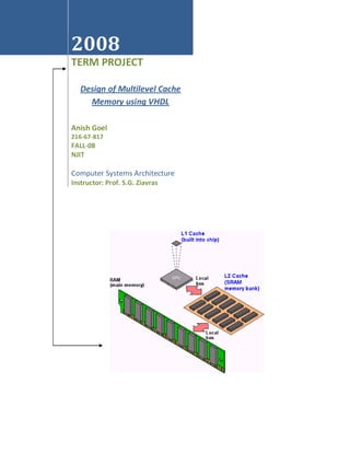
  • 1. 2008 TERM PROJECT Design of Multilevel Cache Memory using VHDL Anish Goel 216-67-817 FALL-08 NJIT Computer Systems Architecture Instructor: Prof. S.G. Ziavras
  • 2. Page |2 CONTENTS 1. Problem Statement……………………………………………………………………………………………. 4 2. Design Description and Block Diagram……………………………………………………………….. 5 3. Design Approach……………………………………………………………………………………………….. 10 4. Results………………………………………………………………………………………………………………. 11 5. Observations……………………………………………………………………………………………………… 14 Appendix A: VHDL Code…………………………………………………………………………………………… 15 Appendix B: Simulation Results………………………………………………………………………………… 29 Appendix C: Synthesis Results………………………………………………………………………………….. 31 References
  • 3. Page |3 List of Figures Figure 1: System block layout………………………………………………………………………………………………………… 5 Figure 2: L1 Cache Block Diagram………………………………………………………………………………………………….. 7 Figure 3: L2 Cache Block Diagram………………………………………………………………………………………………….. 8 Figure 4: Cache Controller Signals…………………………………………………………………………………………………. 9 Figure 5: Simulation Results L1 Cache……………………………………………………………………………………………. 11 Figure 6: Simulation Results L2 Cache……………………………………………………………………………………………. 12 Figure 7: Simulation Results Cache Controller………………………………………………………………………………. 13
  • 4. Page |4 1. Problem Statement: To design a multilevel cache memory for a uni-processor system using VHDL. Cache Memory Specifications: CACHE SIZE MAPPING L1 Cache 16KB 4-way set associative L2 Cache 128KB 8-way set associative Features:  Unified I & D cache at both levels L1 and L2  Set associative mapping  Write through policy  Common cache controller for L1 and L2 The project aims at designing the above mentioned memory hierarchy of cache memories for uni-processor system and obtain the simulation results using the ModelSim platform. In addition, the Xilinx ISE platform depicts the synthesized system for the designed VHDL code.
  • 5. Page |5 2. Design Description: The design consists of two levels of cache memory as Level 1 (L1) and Level 2 (L2) and a cache controller that communicates between microprocessor and cache memories to carry out all memory related operations. The size and specifications of the cache memories are stated in the problem specification above and the design approach is described in the next section. Figure 1 shows the block diagram of the designed system. Microprocessor Cache Controller System Busses Level 1 Cache Level 2 Memory Cache Memory Figure 1: System block layout The functionality of the design is explained below: 1. Cache controller receives the address that microprocessor wants to access. 2. Cache controller looks for the address in the L1 cache. 3. If the address is in L1 cache (cache hit occurs in L1), the data from the location is provided to the microprocessor via the data bus. 4. If the address is not found in L1 cache i.e. cache miss occurs. 5. Cache controller looks for the same address in the L2 cache. 6. If the address is found in L2 cache (cache hit occurs in L2), the data from the location is provided to the microprocessor and the same data is also replaced in the L1 cache. 7. If the address is not found in L2 cache i.e. cache miss occurs in L2. 8. The controller has to request the same address in the main memory. This functionality is not modeled in the project, here the cache controller gives a signal to the microprocessor that a cache miss has occurred in the L2 cache. The microprocessor should then take appropriate action.
  • 6. Page |6 L1 and L2 specifications: Physical Address: 32-bit L1 Cache: Refer to figure 2 for the internal architecture of L1 cache. Address Format (fields) Word Size: 32-bit (4 bytes) Tag: 22-bit Set Address: 8-bit Word: 2-bit Physical Memory Address: 32-bit TAG: 22 bit SET: 8-bit Address WORD: 2-bit L1 Cache Memory: 16KB 4-way set associative unified instruction and data cache. Total number of sets: 256*4 = 1024 sets L2 Cache: Refer to figure 3 for the internal architecture of L2 cache. Address Format (fields) Word Size: 32-bit (4 bytes) Tag: 20-bit Set Address: 10-bit Word: 2-bit Physical Memory Address: 32-bit TAG: 20 bit SET: 10-bit Address WORD: 2-bit L2 Cache Memory: 128KB 8-way set associative unified instruction and data cache. Total number of sets: 1024x8 = 8192 sets
  • 7. Page |7 L1 Cache Memory Architecture A0-A31 32-bit Address Bus W WA WA Y Word Address A0-A1 W AY 3 A Y 2 T Y 1 A Set Address A2-A9 0 G A2-A9 A2-A9 A C Set 0: T0-T21 D Set 0: D0-D127 D A A A D C Set 1: T0-T21 T Set 1: D0-D127 R H … A … E E S M S D E I M R. O Set 255: T0-T21 R Set 255: D0-D127 Y A10-A31 T0-T21 Enable Data (4 Words) A0-A1 Tag Address Comparator Data buffer Hit/Miss 32-bit Data Figure 2: L1 Cache Block Diagram
  • 8. Page |8 L2 Cache Memory Architecture A0-A31 32-bit Address Bus WAY7 W Word Address A0-A1 W A A Y Y 1 T 0 A Set Address A2-A11 G A2-A11 A2-A11 Set 0: T0-T19 Set 0: D0-D127 A C D D A Set 1: T0-T19 A Set 1: D0-D127 A D C … T … R H A E E S M S D E I M R. Set 1023: T0-T19 O Set 1023: D0-D127 R Y A10-A31 T0-T19 Data (4 Words) A0-A1 Enable Tag Address Comparator Data buffer Hit/Miss 32-bit Data Figure 3: L2 Cache Block Diagram
  • 9. Page |9 Cache Controller The following diagram depicts all the signals of the cache controller that are used to carry out all the memory related operations between microprocessor and L1 and L2 cache. Reset Controller Controller Busy DAV_L1 DAV_L2 Address Request From microprocessor Cache Address Bus A31 –AA0 To Main Memory Cache Hit/Miss (L1) From each Block Controller Data bus D0-D31 L1 Enable Read Write L2 Enable Cache Hit/Miss (L2) From each Bloc Address and Data Bus to L1 L2 Cache Figure 4: Cache Controller Signals DAV_L1/L2: Data valid from L1 or L2 cache memory on the system data bus when a cache hit occurs in the corresponding block.
  • 10. P a g e | 10 3. Design Approach: The project is designed using mixed style of modeling in VHDL. ModelSim SE PLUS 6.2c platform from Mentor Graphics is used as the design platform and simulator. To achieve the synthesis of the design, Xilinx ISE 9.1i platform is used. The basic storage element in the memory is modeled using a D flip-flop. Each D flip-flop stores a single bit. Arrays of this storage element is constructed using structural style of modeling in VHDL to form registers (for example: 22 bit tag register) and these registers are again used to create the complete memory array. The memory consists of L1 cache that is arranged as follows: L1 Cache capacity details Cache data memory: Word size = 32 bits Line size = 128 bits (4 words) No. of lines = 256 per block Thus total capacity is = 256*4 = 1KWords (4KB) {Per way} Thus for 4 way set associative cache memory: Total capacity is 1KWord x 4 = 4KWord (16KB) Cache Tag memory: Tag size = 22 bits Cache Tag comparator: 22 bit comparator Input Output Buffer: 128 bits The L2 cache is also designed using the same concept except for the difference that the size of the L2 cache is much larger then L1 cache and also it is a 8-way set associative cache. L2 Cache capacity details Cache data memory: Word size = 32 bits Line size = 128 bits (4 words) No. of lines = 1024 per block Thus total capacity is = 1024*4 = 4KWords (16KB) {per way} Thus for 4 way set associative cache memory: Total capacity is 4KWord x 8 = 32KWord (128KB) Cache Tag memory: Tag size = 20 bits Cache Tag comparator: 20 bit comparator Input Output Buffer: 128 bits All the operations in the L1 and L2 cache are guided by a cache controller. Any address request from the microprocessor is first directed to the cache controller. The cache controller then looks for the address in the L1 cache, if a cache hit occurs in L1 the data from the requested location is transferred to the microprocessor. In case a cache miss occurs in L1, the cache controller looks for the same address in L2 cache and if a cache hit occurs in L2, the controllers transfers the same data to the microprocessor as well as the L1 cache.
  • 11. P a g e | 11 4. Simulation Results: The following figures depict the simulation results of the higher entities like the L1, L2 cache and cache controller. The results of discrete blocks like memory decoder, cache tag comparator etc. is shown in appendix B. L1 Cache: Cache Miss in L1 Figure 5: Simulation Results L1 Cache
  • 12. P a g e | 12 L2 Cache Cache hit in Way 5 L2 cache (for same address) Figure 6: Simulation Results L2 Cache
  • 13. P a g e | 13 Cache Controller: 1 2 3 Figure 7: Simulation Results Cache Controller 1: Cache Hit in L1 cache for specified address. 2: Cache miss in L1 cache for different address then address in instance 1 3: Cache hit in L2 cache for same address as in address in instance 2 Important Note: The above simulation results are obtained with respect to specified locations to test the functionality of the memory hierarchy. The data was previously stored on these addresses. However the address request from the microprocessor depends in the program code. Also the microprocessor generates address continuously and randomly based on the nature of the program. Thus to test the performance of this cache a complete hardware is needed that will carry out the functionality of the microprocessor.
  • 14. P a g e | 14 5. Observations: 1. Level 1 and Level 2 cache memories give the correct results at the output signals cache_hit and Cache_miss if a match occurs between the tag part of the address requested by the microprocessor and the corresponding entry in the cache directory. 2. The read/write pins do not have any signals (Logic levels) on them as it is to be specified by the microprocessor as to a read operation or a write operation is to occur. 3. The cache controller delivers the appropriate signals to the cache memories L1 and L2 to match the tag part of the address requested by the microprocessor and if a cache hit occurs, it indicates this to the microprocessor by means of DAV_L1 or DAV_L2 (Data Valid) that the data over the data bus is valid data requested by the microprocessor from the requested address. 4. A cache hit in L1 or L2 cache directly outputs the data from the requested address to the data bus. This is not indicated in the above simulation result as many of the signals are activated in the internal architecture and not visible in the higher level hierarchy. 5. To observe the results mention in the point 4 above, some of the blocks like tag comparator and output buffer needs to be simulated separately. Some of these results are indicated in Appendix B.
  • 15. P a g e | 15 Appendix A: VHDL Codes The following are the VHDL codes for all the .vhd files in the project design. Files related to L1 and L2 cache memories. D Flip-Flop library IEEE; use IEEE.STD_LOGIC_1164.ALL; use IEEE.STD_LOGIC_ARITH.ALL; use IEEE.STD_LOGIC_UNSIGNED.ALL; entity dff is Port ( d : in std_logic; clk : in std_logic; q : out std_logic; en : in std_logic); end dff; architecture Behavioral of dff is begin process(clk) begin if en='1' then if clk'event and clk='1' then q<= d; end if; else q<= 'Z'; end if; end process; end Behavioral; Cache Data Line: 128 bits (4, 32-bit words) library IEEE; use IEEE.STD_LOGIC_1164.ALL; use IEEE.STD_LOGIC_ARITH.ALL; use IEEE.STD_LOGIC_UNSIGNED.ALL; entity reg_128_data is Port ( D : in std_logic_vector(127 downto 0); clk : in std_logic; Q : out std_logic_vector(127 downto 0); en : in std_logic); end reg_128_data; architecture Behavioral of reg_128_data is component dff
  • 16. P a g e | 16 port(d: in std_logic; q: out std_logic; clk: in std_logic; en : in std_logic); end component; signal outbuf: std_logic_vector(127 downto 0); begin gen: for i in 0 to 127 generate mem: dff port map (d(i),q(i),clk,en); end generate; end Behavioral; Data Block L1 Cache (256 Cache Lines) library IEEE; use IEEE.STD_LOGIC_1164.ALL; use IEEE.STD_LOGIC_ARITH.ALL; use IEEE.STD_LOGIC_UNSIGNED.ALL; --This block generates 256x32 cache data memory entity data_mem is Port ( Din : in std_logic_vector(127 downto 0); Dout : out std_logic_vector(127 downto 0); EN : in std_logic_vector(255 downto 0); clk: in std_logic); end data_mem; architecture Behavioral of data_mem is component reg_128_data Port ( D : in std_logic_vector(127 downto 0); clk : in std_logic; Q : out std_logic_vector(127 downto 0); en : in std_logic); end component; begin GEN_array: for i in 0 to 255 generate REGS: reg_128_data port map (Din(127 downto 0),clk,Dout(127 downto 0),EN(i)); end generate; end Behavioral; 4:16 decoder library IEEE; use IEEE.STD_LOGIC_1164.ALL; use IEEE.STD_LOGIC_ARITH.ALL; use IEEE.STD_LOGIC_UNSIGNED.ALL; entity decoder4to16 is Port ( D : in std_logic_vector(3 downto 0); E : out std_logic_vector(15 downto 0);
  • 17. P a g e | 17 F : in std_logic); end decoder4to16; architecture Behavioral of decoder4to16 is begin process(D,F) begin if F='1' then case D is when"0000"=> E <= (others =>'0'); E(0) <= '1'; when"0001"=> E <= (others =>'0'); E(1) <= '1'; when"0010"=> E <= (others =>'0'); E(2) <= '1'; when"0011"=> E <= (others =>'0'); E(3) <= '1'; when"0100"=> E <= (others =>'0'); E(4) <= '1'; when"0101"=> E <= (others =>'0'); E(5) <= '1'; when"0110"=> E <= (others =>'0'); E(6) <= '1'; when"0111"=> E <= (others =>'0'); E(7) <= '1'; when"1000"=> E <= (others =>'0'); E(8) <= '1'; when"1001"=> E <= (others =>'0'); E(9) <= '1'; when"1010"=> E <= (others =>'0'); E(10) <= '1'; when"1011"=> E <= (others =>'0'); E(11) <= '1'; when"1100"=> E <= (others =>'0'); E(12) <= '1';
  • 18. P a g e | 18 when"1101"=> E <= (others =>'0'); E(13) <= '1'; when"1110"=> E <= (others =>'0'); E(14) <= '1'; when others => E <= (others =>'0'); E(15) <= '1'; end case; end if; end process; end Behavioral; Memory Decoder: 8:256 decoder library IEEE; use IEEE.STD_LOGIC_1164.ALL; use IEEE.STD_LOGIC_ARITH.ALL; use IEEE.STD_LOGIC_UNSIGNED.ALL; --This Block Generates a 8:2^8 decoder entity mem_decoder is port(S: in std_logic_vector(7 downto 0); EN: out std_logic_vector(255 downto 0); Mem_EN: in std_logic); end mem_decoder; architecture Behavioral of mem_decoder is component decoder4to16 is Port ( D : in std_logic_vector(3 downto 0); E : out std_logic_vector(15 downto 0); F : in std_logic); end component; signal C1: std_logic_vector(15 downto 0); begin stage1: decoder4to16 port map(S(7 downto 4),C1(15 downto 0),Mem_EN); struct: for i in 16 downto 1 generate stage2: decoder4to16 port map (S(3 downto 0),EN(((16*i)-1) downto ((16*i)-16)),C1(i-1)); end generate; end Behavioral; Input Output Buffer: library IEEE; use IEEE.STD_LOGIC_1164.ALL;
  • 19. P a g e | 19 use IEEE.STD_LOGIC_ARITH.ALL; use IEEE.STD_LOGIC_UNSIGNED.ALL; entity inout_buf is Port ( A : inout std_logic_vector(127 downto 0); B : inout std_logic_vector(127 downto 0); WR : in std_logic; RD : in std_logic); end inout_buf; architecture Behavioral of inout_buf is begin process(WR,RD) begin if WR='1' then B<= A; else B<= (others => ‘Z’); if RD='1' then A<= B; else A<=(others => ‘Z’); end if; end if; end process; end Behavioral; Address Fields: library IEEE; use IEEE.STD_LOGIC_1164.ALL; use IEEE.STD_LOGIC_ARITH.ALL; use IEEE.STD_LOGIC_UNSIGNED.ALL; entity address_field is port(addr: in std_logic_vector(31 downto 0); word: out std_logic_vector(1 downto 0); set: out std_logic_vector(7 downto 0); tag: out std_logic_vector(21 downto 0); sep: in std_logic); end address_field; architecture Behavioral of address_field is begin process(addr) begin if sep = '1' then word <= addr (1 downto 0);
  • 20. P a g e | 20 set <= addr (9 downto 2); tag <= addr (31 downto 10); end if; end process; end Behavioral; CACHE L1: library ieee; use ieee.std_logic_1164.all; use IEEE.std_logic_arith.all; use ieee.std_logic_unsigned.all; entity memory_L1 is port(Add: in std_logic_vector(7 downto 0); Data: inout std_logic_vector(127 downto 0); RD,WR,CLK,EN: in std_logic); end memory_L1; architecture struct of memory_L1 is component data_mem is Port ( Din : in std_logic_vector(127 downto 0); Dout : out std_logic_vector(127 downto 0); EN : in std_logic_vector(255 downto 0); clk: in std_logic); end component; component inout_buf is Port ( A : inout std_logic_vector(127 downto 0); B : inout std_logic_vector(127 downto 0); WR : in std_logic; RD : in std_logic); end component; component mem_decoder is port(S: in std_logic_vector(7 downto 0); EN: out std_logic_vector(255 downto 0); Mem_EN: in std_logic); end component; signal int: std_logic_vector(255 downto 0); signal dat: std_logic_vector(127 downto 0); begin decoder: mem_decoder port map (Add,int,EN); buff: inout_buf port map (Data,dat,WR,RD); mem: data_mem port map (dat,Data,int,CLK); end struct;
  • 21. P a g e | 21 Tag Register : 22 –bit library IEEE; use IEEE.STD_LOGIC_1164.ALL; use IEEE.STD_LOGIC_ARITH.ALL; use IEEE.STD_LOGIC_UNSIGNED.ALL; ---- Uncomment the following library declaration if instantiating ---- any Xilinx primitives in this code. --library UNISIM; --use UNISIM.VComponents.all; entity tag_data_L1 is Port ( D : in std_logic_vector(21 downto 0); clk : in std_logic; Q : out std_logic_vector(21 downto 0); en : in std_logic); end tag_data_L1; architecture Behavioral of tag_data_L1 is component dff port(d: in std_logic; q: out std_logic; clk: in std_logic; en : in std_logic); end component; signal outbuf: std_logic_vector(21 downto 0); begin gen: for i in 0 to 21 generate mem: dff port map (d(i),q(i),clk,en); end generate; end Behavioral; Tag Memory : 256x22 bit library IEEE; use IEEE.STD_LOGIC_1164.ALL; use IEEE.STD_LOGIC_ARITH.ALL; use IEEE.STD_LOGIC_UNSIGNED.ALL; --This block generates 255x28 data cache tag memory entity tag_mem is Port ( Din : in std_logic_vector(21 downto 0); Dout : out std_logic_vector(21 downto 0); EN : in std_logic_vector(255 downto 0);
  • 22. P a g e | 22 clk: in std_logic); end tag_mem; architecture Behavioral of tag_mem is component tag_data_L1 Port ( D : in std_logic_vector(21 downto 0); clk : in std_logic; Q : out std_logic_vector(21 downto 0); en : in std_logic); end component; begin GEN_array: for i in 0 to 255 generate REGS: tag_data_L1 port map (Din(21 downto 0),clk,Dout(21 downto 0),EN(i)); end generate; end Behavioral; Cache Tag Buffer: library IEEE; use IEEE.STD_LOGIC_1164.ALL; use IEEE.STD_LOGIC_ARITH.ALL; use IEEE.STD_LOGIC_UNSIGNED.ALL; entity inout_buf_tag is Port ( A : inout std_logic_vector(21 downto 0); B : inout std_logic_vector(21 downto 0); WR : in std_logic; RD : in std_logic); end inout_buf_tag; architecture Behavioral of inout_buf_tag is begin process(WR,RD) begin if WR='1' then B<= A; else B<= "ZZZZZZZZZZZZZZZZZZZZZZZ"; if RD='1' then A<= B; else A<="ZZZZZZZZZZZZZZZZZZZZZZZ"; end if; end if; end process; end Behavioral;
  • 23. P a g e | 23 Cache Tag Memory: library ieee; use ieee.std_logic_1164.all; use IEEE.std_logic_arith.all; use ieee.std_logic_unsigned.all; entity cache_tag_data_L1 is port(Add: in std_logic_vector(7 downto 0); tag: inout std_logic_vector(21 downto 0); RD,WR,CLK,EN: in std_logic); end cache_tag_data_L1; architecture struct of cache_tag_data_L1 is component tag_mem is Port ( Din : in std_logic_vector(21 downto 0); Dout : out std_logic_vector(21 downto 0); EN : in std_logic_vector(255 downto 0); clk: in std_logic); end component; component inout_buf_tag is Port ( A : inout std_logic_vector(21 downto 0); B : inout std_logic_vector(21 downto 0); WR : in std_logic; RD : in std_logic); end component; component mem_decoder is port(S: in std_logic_vector(7 downto 0); EN: out std_logic_vector(255 downto 0); Mem_EN: in std_logic); end component; signal int: std_logic_vector(255 downto 0); signal dat: std_logic_vector(21 downto 0); begin decoder: mem_decoder port map (Add,int,EN); buff: inout_buf_tag port map (tag,dat,WR,RD); mem: tag_mem port map (dat,tag,int,CLK); end struct;
  • 24. P a g e | 24 Cache Tag Comparator: library IEEE; use IEEE.STD_LOGIC_1164.ALL; use IEEE.STD_LOGIC_ARITH.ALL; use IEEE.STD_LOGIC_UNSIGNED.ALL; --This block compares the two addresses and produces a cache hit/miss signal entity tag_comparator is port( Addr_req: in std_logic_vector (21 downto 0); Addr_tag: in std_logic_vector (21 downto 0); tag_hit: out std_logic; EN: in std_logic); end tag_comparator; architecture Behavioral of tag_comparator is begin process(Addr_req,Addr_tag,EN) begin tag_hit <= '0'; if EN = '1' then if Addr_req = Addr_tag then tag_hit <= '1'; end if; end if; end process; end Behavioral; L1 DATA BUFFER: library IEEE; use IEEE.STD_LOGIC_1164.ALL; use IEEE.STD_LOGIC_ARITH.ALL; use IEEE.STD_LOGIC_UNSIGNED.ALL; -- 128 bit data buffer for L1 data cache entity data_buff_L1 is Port ( Din : in std_logic_vector(127 downto 0); Dout : out std_logic_vector(31 downto 0); EN : in std_logic_vector(1 downto 0); clk: in std_logic); end data_buff_L1; architecture behaviour of data_buff_L1 is begin process(clk,EN) begin if clk'event and clk = '1'
  • 25. P a g e | 25 then case EN is when "00" => Dout <= Din(127 downto 96); when "01" => Dout <= Din(95 downto 64); when "10" => Dout <= Din(63 downto 32); when others => Dout <= Din(31 downto 0); end case; end if; end process; end behaviour; L1 Data Cache: Way 0 library ieee; use ieee.std_logic_1164.all; use ieee.std_logic_arith.all; use IEEE.STD_LOGIC_UNSIGNED.ALL; entity L1_data_way0 is port( Add: in std_logic_vector(31 downto 0); data_out : out std_logic_vector(31 downto 0); cache_hit: out std_logic; clk,EN,RD,WR: in std_logic); end L1_data_way0; architecture structure of L1_data_way0 is signal F1: std_logic_vector(1 downto 0); signal F2: std_logic_vector(7 downto 0); signal F3: std_logic_vector(21 downto 0); signal data: std_logic_vector(127 downto 0); signal tag: std_logic_vector(21 downto 0); signal select_add: std_logic_vector(255 downto 0); component memory_L1 is port(Add: in std_logic_vector(7 downto 0); Data: inout std_logic_vector(127 downto 0); RD,WR,CLK,EN: in std_logic); end component; component cache_tag_data_L1 is port(Add: in std_logic_vector(7 downto 0); tag: inout std_logic_vector(21 downto 0); RD,WR,CLK,EN: in std_logic); end component; component address_field is port(addr: in std_logic_vector(31 downto 0); word: out std_logic_vector(1 downto 0);
  • 26. P a g e | 26 set: out std_logic_vector(7 downto 0); tag: out std_logic_vector(21 downto 0); sep: in std_logic); end component; L1 4-way set associative cache: Main hierarchy for L1 cache memory. library ieee; use ieee.std_logic_1164.all; use ieee.std_logic_arith.all; use IEEE.STD_LOGIC_UNSIGNED.ALL; entity L1_cache is port( Add: in std_logic_vector(31 downto 0); data_out : inout std_logic_vector(31 downto 0); cache_hit: out std_logic_vector(3 downto 0); clk,RD,WR: in std_logic; EN: in std_logic_vector(3 downto 0)); end L1_cache; architecture structure of L1_cache is component L1_data_way0 is port( Add: in std_logic_vector(31 downto 0); data_out : inout std_logic_vector(31 downto 0); cache_hit: out std_logic; clk,EN,RD,WR: in std_logic); end component; begin sets: for i in 0 to 3 generate struct: L1_data_way0 port map (Add,data_out,cache_hit(i),clk,EN(i),RD,WR); end generate; end structure; L2 Cache memory uses all the above specified .vhd files. Changes are made accordingly to increase the register size and capacity.
  • 27. P a g e | 27 Cache Controller VHDL code: library ieee; use ieee.std_logic_1164.all; use ieee.std_logic_arith.all; use IEEE.STD_LOGIC_UNSIGNED.ALL; entity cache_controller is Port (add_req: in std_logic_vector(31 downto 0); C_busy: out std_logic; C_reset,clk,EN:in std_logic; L1_miss,L2_miss,RD: out std_logic; Add_L1: out std_logic_vector(31 downto 0); DAV_L1: out std_logic; cache_hit_l1: in std_logic_vector(3 downto 0); Add_L2: out std_logic_vector(31 downto 0); DAV_L2: out std_logic; cache_hit_l2: in std_logic_vector(7 downto 0)); end cache_controller; Architecture behaviour of cache_controller is signal C1,C2: std_logic_vector(3 downto 0); begin process(add_req,EN) begin if clk'event and clk='1' then if EN = '1' then Add_L1 <= add_req; if (cache_hit_l1(0)='1' or cache_hit_l1(1)='1' or cache_hit_l1(2)='1' or cache_hit_l1(3)='1') then L1_miss <= '0'; DAV_l1<='1'; else L1_miss <= '1'; Add_L2 <= add_req; if (cache_hit_l2(0)='1' or cache_hit_l2(1)='1' or cache_hit_l2(2)='1' or cache_hit_l2(3)='1' or cache_hit_l2(4)='1' or cache_hit_l2(5)='1' or cache_hit_l2(6)='1' or cache_hit_l2(7)='1') then L2_miss <= '0'; DAV_l2<='1'; else L2_miss <= '1'; if clk'event and clk='1' then c1<=c1+1; Add_L2<=add_req+1; RD <=clk; else
  • 28. P a g e | 28 L2_miss <= '1'; end if; end if; end if; end if; end if; end process; end behaviour;
  • 29. P a g e | 29 Appendix B: Simulation Results of Discrete Blocks  Data Buffer L1 Cache 32 Bit word Output selected using A0-A1 Address Lines  Cache Tag Comparator Cache Hit Cache Miss
  • 30. P a g e | 30  Address Field Separator  Memory Decoder
  • 31. P a g e | 31 Appendix C: Synthesis Results L1 Cache Memory Signal Description Add(31:0) 32 bit address from microprocessor Clk: Clock input EN: Memory enable/select signal RD,WR: Read, Write Signal Cache_hit: cache hit/miss signal Data_out(31:0): Bi-directional data bus L1 Cache Memory Block generated using Synthesis Tool Internal Architecture: Includes Blocks:  Address field Separator  Cache data memory  Cache Tag memory  Cache tag comparator  Input/output buffer. Internal Architecture of L1 Cache memory Block L2 cache memory is identical to the L1 cache memory with only difference in number of sets per blocks and total number of blocks.
  • 32. P a g e | 32 Cache Controller The figure depicts all the control signals and buses of the cache controller of the system. Add_req: Address request from the microprocessor Cache_hit_l1(3:0): cache hit from L1 cache memory block Cache_hit_l2(7:0): cache hit from L2 cache memory block Add_L1(31:0): Address bus to L1 cache Add_L2(31:0): Address bus to L2 cache C_busy: Cache controller busy (status signal) Clk: Clock input DAV_L1/L2: Data valid on data bus from respective cache memory C_reset: Reset Cache controller L1/L2_miss: Cache miss from L1/L2 cache RD: Read Cache controller status The figure below shows the internal architecture of the cache controller synthesized using the Xilinx ISE 9.1i platform. Cache Controller internal Architecture
  • 33. P a g e | 33  A view of the Xilinx ISE 9.1i Synthesis Tool window  A view of the ModelSim SE Plus 6.2c Simulation Tool window
  • 34. P a g e | 34 References  Computer Architecture and Organization By: John P. Hayes. (Mc Graw Hill publication)  Fundamentals of Digital Logic with VHDL design By: Stephen Brown & Zvonko Vranesic (TATA Mc Graw Hill)  A Circuit Design of 32KByte Integrated Cache Memory. TOSHIBA Corporation, TOSHIBA Microcomputer Eng.Corp.  http://www.ece.cmu.edu/~ece741  http://en.kioskea.net/pc/memoire.php3  Computer Architecture - A Quantitative Approach, Fourth Edition by John L. Hennessy and David A. Patterson  Advanced Computer Architecture: Parallelism, Scalability, Programmability By Kai Hwang  http://web.njit.edu/~rlopes/cache-performance.pdf  Lecture notes on memory hierarchy design by Prof. S.G. Ziavras including http://web.njit.edu/~ziavras/ECE690-NEW/SYLLABUS-NOTES/CH-5-APP-C/AppC-ch-5-m1- Ziavras.pdf  http://cs.uccs.edu/~cs520/S99ch5.PDF  High performance memories. By : Betty Prince