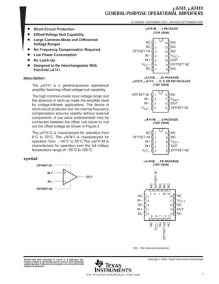
SlideShare une entreprise Scribd logo
1  sur  12
Télécharger pour lire hors ligne
µA741, µA741Y
                                                                                       GENERAL-PURPOSE OPERATIONAL AMPLIFIERS
                                                                                                              SLOS094B – NOVEMBER 1970 – REVISED SEPTEMBER 2000

    D      Short-Circuit Protection                                                                                        µA741M . . . J PACKAGE

    D      Offset-Voltage Null Capability
                                                                                                                                (TOP VIEW)

    D      Large Common-Mode and Differential
                                                                                                                       NC                       NC
           Voltage Ranges                                                                                                         1       14
                                                                                                                       NC                       NC
    D      No Frequency Compensation Required                                                                   OFFSET N1
                                                                                                                                  2
                                                                                                                                  3
                                                                                                                                          13
                                                                                                                                          12    NC
    D      Low Power Consumption                                                                                      IN –        4       11    VCC +
    D      No Latch-Up                                                                                                IN +        5       10    OUT
    D      Designed to Be Interchangeable With                                                                      VCC –         6        9    OFFSET N2
           Fairchild µA741                                                                                             NC         7        8    NC

description                                                                                                           µA741M . . . JG PACKAGE
                                                                                                               µA741C, µA741I . . . D, P, OR PW PACKAGE
         The µA741 is a general-purpose operational                                                                         (TOP VIEW)
         amplifier featuring offset-voltage null capability.
                                                                                                               OFFSET N1          1        8    NC
         The high common-mode input voltage range and
         the absence of latch-up make the amplifier ideal                                                            IN –         2        7    VCC+
         for voltage-follower applications. The device is                                                            IN +         3        6    OUT
         short-circuit protected and the internal frequency                                                        VCC –          4        5    OFFSET N2
         compensation ensures stability without external
         components. A low value potentiometer may be                                                                     µA741M . . . U PACKAGE
         connected between the offset null inputs to null                                                                      (TOP VIEW)
         out the offset voltage as shown in Figure 2.
         The µA741C is characterized for operation from                                                                NC         1       10    NC
         0°C to 70°C. The µA741I is characterized for                                                           OFFSET N1         2        9    NC
         operation from – 40°C to 85°C.The µA741M is                                                                  IN –        3        8    VCC +
         characterized for operation over the full military                                                           IN +        4        7    OUT
         temperature range of – 55°C to 125°C.                                                                      VCC –         5        6    OFFSET N2

symbol
                                                                                                                          µA741M . . . FK PACKAGE
              OFFSET N1                                                                                                        (TOP VIEW)
                                                                                                                                OFFSET N1


                          IN +                +
                                                                        OUT
                           IN –               –
                                                                                                                                NC

                                                                                                                                NC
                                                                                                                                NC
                                                                                                                                NC


              OFFSET N2
                                                                                                                                3 2 1 20 19
                                                                                                                    NC      4              18        NC
                                                                                                                   IN –     5                  17    VCC +
                                                                                                                    NC      6                  16    NC
                                                                                                                   IN +     7                  15    OUT
                                                                                                                    NC      8               14       NC
                                                                                                                                9 10 11 12 13
                                                                                                                                    VCC–

                                                                                                                                OFFSET N2
                                                                                                                                      NC

                                                                                                                                      NC

                                                                                                                                      NC


                                                                                                                NC – No internal connection


PRODUCTION DATA information is current as of publication date.                                                              Copyright © 2000, Texas Instruments Incorporated
Products conform to specifications per the terms of Texas Instruments
standard warranty. Production processing does not necessarily include
testing of all parameters.


                                                                        POST OFFICE BOX 655303   • DALLAS, TEXAS 75265                                                    1
µA741, µA741Y
GENERAL-PURPOSE OPERATIONAL AMPLIFIERS
SLOS094B – NOVEMBER 1970 – REVISED SEPTEMBER 2000

                                                          AVAILABLE OPTIONS
                                                            PACKAGED DEVICES
                                                                                                                     CHIP
           TA             SMALL           CHIP        CERAMIC       CERAMIC           PLASTIC               FLAT     FORM
                                                                                                 TSSOP
                         OUTLINE        CARRIER         DIP            DIP              DIP                 PACK      (Y)
                                                                                                  (PW)
                           (D)            (FK)          (J)           (JG)              (P)                  (U)
       0°C to 70°C        µA741CD                                                     µA741CP   µA741CPW             µA741Y
     – 40°C to 85°C       µA741ID                                                     µA741IP
     – 55°C to 125°C                   µA741MFK       µA741MJ      µA741MJG                                µA741MU
    The D package is available taped and reeled. Add the suffix R (e.g., µA741CDR).


schematic
                                                                                                                       VCC+


                IN –


                                                                                                                       OUT
                IN+


      OFFSET N1
      OFFSET N2


                                                                                                                       VCC –


                                                           Component Count
                                                           Transistors         22
                                                           Resistors           11
                                                           Diode                1
                                                           Capacitor            1


2                                              POST OFFICE BOX 655303   • DALLAS, TEXAS 75265
µA741, µA741Y
                                                        GENERAL-PURPOSE OPERATIONAL AMPLIFIERS
                                                                               SLOS094B – NOVEMBER 1970 – REVISED SEPTEMBER 2000


µA741Y chip information
    This chip, when properly assembled, displays characteristics similar to the µA741C. Thermal compression or
    ultrasonic bonding may be used on the doped-aluminum bonding pads. Chips may be mounted with conductive
    epoxy or a gold-silicon preform.

                          BONDING PAD ASSIGNMENTS
                                                                                                               VCC+
                                                                                                                 (7)
                                                 (7)           (6)                           IN +
                                                                                                    (3)
                                                                                                           +           (6)
                                                                                                    (2)                      OUT
                                                                                             IN –          –
                                                                                    OFFSET N1       (1)          (4)
                    (8)
                                                                                   OFFSET N2        (5)        VCC –


        45
                                                               (5)


              (1)                                                                         CHIP THICKNESS: 15 TYPICAL
                                                               (4)
                                                                                          BONDING PADS: 4 × 4 MINIMUM
                                                                                          TJmax = 150°C.
                             (2)                         (3)                              TOLERANCES ARE ± 10%.
                                                                                          ALL DIMENSIONS ARE IN MILS.
                                    36


                                         POST OFFICE BOX 655303   • DALLAS, TEXAS 75265                                            3
µA741, µA741Y
GENERAL-PURPOSE OPERATIONAL AMPLIFIERS
SLOS094B – NOVEMBER 1970 – REVISED SEPTEMBER 2000


absolute maximum ratings over operating free-air temperature range (unless otherwise noted)†
                                                                                                     µA741C             µA741I     µA741M       UNIT
 Supply voltage, VCC+ (see Note 1)                                                                      18                22          22         V
 Supply voltage, VCC – (see Note 1)                                                                    –18              – 22        – 22         V
 Differential input voltage, VID (see Note 2)                                                          ±15               ±30         ±30         V
 Input voltage, VI any input (see Notes 1 and 3)                                                       ±15               ±15         ±15         V
 Voltage between offset null (either OFFSET N1 or OFFSET N2) and VCC –                                 ±15              ±0.5        ±0.5         V
 Duration of output short circuit (see Note 4)                                                      unlimited       unlimited      unlimited
 Continuous total power dissipation                                                                             See Dissipation Rating Table
 Operating free-air temperature range, TA                                                             0 to 70       – 40 to 85    – 55 to 125    °C
 Storage temperature range                                                                          – 65 to 150    – 65 to 150    – 65 to 150    °C
 Case temperature for 60 seconds                                       FK package                                                    260         °C
 Lead temperature 1,6 mm (1/16 inch) from case for 60 seconds          J, JG, or U package                                           300         °C
 Lead temperature 1,6 mm (1/16 inch) from case for 10 seconds         D, P, or PW package      260            260                           °C
† Stresses beyond those listed under “absolute maximum ratings” may cause permanent damage to the device. These are stress ratings only, and
  functional operation of the device at these or any other conditions beyond those indicated under “recommended operating conditions” is not
  implied. Exposure to absolute-maximum-rated conditions for extended periods may affect device reliability.
NOTES: 1. All voltage values, unless otherwise noted, are with respect to the midpoint between VCC+ and VCC – .
           2. Differential voltages are at IN+ with respect to IN –.
           3. The magnitude of the input voltage must never exceed the magnitude of the supply voltage or 15 V, whichever is less.
           4. The output may be shorted to ground or either power supply. For the µA741M only, the unlimited duration of the short circuit applies
               at (or below) 125°C case temperature or 75°C free-air temperature.

                                                          DISSIPATION RATING TABLE
                         TA ≤ 25°C              DERATING        DERATE              TA = 70°C             TA = 85°C                TA = 125°C
        PACKAGE
                       POWER RATING              FACTOR        ABOVE TA           POWER RATING          POWER RATING             POWER RATING
             D              500 mW               5.8 mW/°C        64°C                 464 mW                   377 mW                N/A
            FK              500 mW              11.0 mW/°C        105°C                500 mW                   500 mW              275 mW
             J              500 mW              11.0 mW/°C        105°C                500 mW                   500 mW              275 mW
            JG              500 mW               8.4 mW/°C          90°C               500 mW                   500 mW              210 mW
             P              500 mW                 N/A               N/A               500 mW                   500 mW                N/A
            PW              525 mW               4.2 mW/°C          25°C               336 mW                     N/A                 N/A
             U              500 mW               5.4 mW/°C          57°C               432 mW                   351 mW              135 mW


4                                                  POST OFFICE BOX 655303   • DALLAS, TEXAS 75265
µA741, µA741Y
                                                                    GENERAL-PURPOSE OPERATIONAL AMPLIFIERS
                                                                                        SLOS094B – NOVEMBER 1970 – REVISED SEPTEMBER 2000


electrical characteristics at specified free-air temperature, VCC± = ±15 V (unless otherwise noted)
                                                    TEST                                       µA741C            µA741I, µA741M
                PARAMETER                                                   TA†                                                        UNIT
                                                 CONDITIONS                            MIN         TYP    MAX    MIN    TYP    MAX
                                                                           25°C                      1      6             1       5
 VIO           Input offset voltage           VO = 0                                                                                   mV
                                                                         Full range                        7.5                    6
 ∆VIO(adj)     Offset voltage adjust range    VO = 0                       25°C                    ± 15                 ± 15           mV
                                                                           25°C                     20    200            20    200
 IIO           Input offset current           VO = 0                                                                                   nA
                                                                         Full range                       300                  500
                                                                           25°C                     80    500            80    500
 IIB           Input bias current             VO = 0                                                                                   nA
                                                                         Full range                       800                  1500
               Common-mode input                                           25°C         ± 12       ± 13          ± 12   ± 13
 VICR                                                                                                                                   V
               voltage range                                             Full range     ± 12                     ± 12
                                              RL = 10 kΩ                   25°C         ± 12       ± 14          ± 12   ± 14
               Maximum peak output            RL ≥ 10 kΩ                 Full range     ± 12                     ± 12
 VOM                                                                                                                                    V
               voltage swing                  RL = 2 kΩ                    25°C         ± 10       ± 13          ± 10   ± 13
                                              RL ≥ 2 kΩ                  Full range     ± 10                     ± 10
               Large-signal differential
                   g   g                      RL ≥ 2 kΩ                    25°C          20        200            50    200
 AVD                                                                                                                                   V/mV
               voltage amplification          VO = ±10 V                 Full range      15                       25
 ri            Input resistance                                            25°C          0.3         2           0.3      2            MΩ
 ro            Output resistance              VO = 0,     See Note 5       25°C                     75                   75             Ω
 Ci            Input capacitance                                           25°C                    1.4                  1.4             pF
               Common-mode rejection
                             j                                             25°C          70         90            70     90
 CMRR                                         VIC = VICRmin                                                                            dB
               ratio                                                     Full range      70                       70
               Supply voltage sensitivity
                    y      g            y                                  25°C                     30    150            30    150
 kSVS                                         VCC = ± 9 V to ± 15 V                                                                    µV/V
               (∆VIO /∆VCC)                                              Full range                       150                  150
 IOS           Short-circuit output current                                25°C                    ± 25   ± 40          ± 25   ± 40    mA
                                                                           25°C                    1.7     2.8          1.7     2.8
 ICC           Supply current                 VO = 0
                                                   0,     No load                                                                      mA
                                                                         Full range                        3.3                  3.3
                                                                           25°C                     50     85            50       85
 PD            Total power dissipation        VO = 0
                                                   0,     No load                                                                      mW
                                                                         Full range                       100                  100
† All characteristics are measured under open-loop conditions with zero common-mode input voltage unless otherwise specified. Full range for
  the µA741C is 0°C to 70°C, the µA741I is – 40°C to 85°C, and the µA741M is – 55°C to 125°C.
NOTE 5: This typical value applies only at frequencies above a few hundred hertz because of the effects of drift and thermal feedback.


operating characteristics, VCC± = ±15 V, TA = 25°C
                                                                                               µA741C            µA741I, µA741M
                PARAMETER                           TEST CONDITIONS                                                                    UNIT
                                                                                       MIN         TYP    MAX    MIN    TYP    MAX
 tr          Rise time                        VI = 20 mV,
                                                        ,                    ,
                                                                    RL = 2 kΩ,                     0.3                  0.3             µs
             Overshoot factor                 CL = 100 pF,          See Figure 1                   5%                   5%
                                              VI = 10 V,            RL = 2 kΩ,
 SR          Slew rate at unity gain                                                               0.5                  0.5            V/µs
                                              CL = 100 pF,          See Figure 1


                                                  POST OFFICE BOX 655303   • DALLAS, TEXAS 75265                                              5
µA741, µA741Y
GENERAL-PURPOSE OPERATIONAL AMPLIFIERS
SLOS094B – NOVEMBER 1970 – REVISED SEPTEMBER 2000


electrical characteristics at specified free-air temperature, VCC± = ±15 V, TA = 25°C (unless
otherwise noted)
                                                                                                                          µA741Y
                                  PARAMETER                                           TEST CONDITIONS                                     UNIT
                                                                                                                   MIN      TYP    MAX
 VIO           Input offset voltage                                               VO = 0                                      1      6    mV
 ∆VIO(adj)     Offset voltage adjust range                                        VO = 0                                    ± 15          mV
 IIO           Input offset current                                               VO = 0                                     20    200    nA
 IIB           Input bias current                                                 VO = 0                                     80    500    nA
 VICR          Common-mode input voltage range                                                                     ± 12     ± 13           V
                                                                                  RL = 10 kΩ                       ± 12     ± 14
 VOM           Maximum peak output voltage swing                                                                                           V
                                                                                  RL = 2 kΩ                        ± 10     ± 13
 AVD           Large-signal differential voltage amplification                    RL ≥ 2 kΩ                         20      200           V/mV
 ri            Input resistance                                                                                    0.3        2           MΩ
 ro            Output resistance                                                  VO = 0,       See Note 5                   75            Ω
 Ci            Input capacitance                                                                                             1.4           pF
 CMRR          Common-mode rejection ratio                                        VIC = VICRmin                     70       90           dB
 kSVS          Supply voltage sensitivity (∆VIO /∆VCC)                            VCC = ± 9 V to ± 15 V                      30    150    µV/V
 IOS           Short-circuit output current                                                                                 ± 25   ± 40   mA
 ICC           Supply current                                                     VO = 0,       No load                      1.7    2.8   mA
 PD           Total power dissipation                                             VO = 0,
                                                                                      No load                           50      85   mW
† All characteristics are measured under open-loop conditions with zero common-mode voltage unless otherwise specified.
NOTE 5: This typical value applies only at frequencies above a few hundred hertz because of the effects of drift and thermal feedback.


operating characteristics, VCC ± = ±15 V, TA = 25°C
                                                                                                                          µA741Y
                                  PARAMETER                                           TEST CONDITIONS                                     UNIT
                                                                                                                   MIN      TYP    MAX
 tr          Rise time                                                            VI = 20 mV,
                                                                                            ,                ,
                                                                                                    RL = 2 kΩ,               0.3           µs
             Overshoot factor                                                     CL = 100 pF,      See Figure 1            5%
                                                                                  VI = 10 V,        RL = 2 kΩ,
 SR          Slew rate at unity gain                                                                                         0.5          V/µs
                                                                                  CL = 100 pF,      See Figure 1


6                                                  POST OFFICE BOX 655303   • DALLAS, TEXAS 75265
µA741, µA741Y
                                                   GENERAL-PURPOSE OPERATIONAL AMPLIFIERS
                                                                          SLOS094B – NOVEMBER 1970 – REVISED SEPTEMBER 2000


                         PARAMETER MEASUREMENT INFORMATION


                           VI
                                                                –                              OUT
                                        IN
                                                                +
                           0V

              INPUT VOLTAGE
                WAVEFDORM
                                                         CL = 100 pF                          RL = 2 kΩ


                                                                               TEST CIRCUIT

                           Figure 1. Rise Time, Overshoot, and Slew Rate


                                    APPLICATION INFORMATION

Figure 2 shows a diagram for an input offset voltage null circuit.

                                       IN +          +
                                                                            OUT
                                       IN –          –              OFFSET N2

                                        OFFSET N1
                                                         10 kΩ


                                                         To VCC –

                                Figure 2. Input Offset Voltage Null Circuit


                                    POST OFFICE BOX 655303   • DALLAS, TEXAS 75265                                        7
µA741, µA741Y
GENERAL-PURPOSE OPERATIONAL AMPLIFIERS
SLOS094B – NOVEMBER 1970 – REVISED SEPTEMBER 2000


                                                                                                              TYPICAL CHARACTERISTICS†

                                                INPUT OFFSET CURRENT                                                                                                                         INPUT BIAS CURRENT
                                                          vs                                                                                                                                          vs
                                                FREE-AIR TEMPERATURE                                                                                                                        FREE-AIR TEMPERATURE
                                    ÏÏÏÏÏ
                                   100

                                    ÏÏÏÏÏVCC+ = 15 V
                                                                                                                                                                          400
                                                                                                                                                                                    VCC+ = 15 V
                                                                                                                                                                                ÏÏÏÏÏ
                                                                                                                                                                                ÏÏÏÏÏ
                                    ÏÏÏÏÏ
                                   90    VCC – = –15 V                                                                                                                    350       VCC – = –15 V
I IO – Input Offset Current – nA


                                    ÏÏÏÏÏ                                                                                                                                       ÏÏÏÏÏ


                                                                                                                                         I IB – Input Bias Current – nA
                                   80
                                                                                                                                                                          300
                                   70

                                   60                                                                                                                                     250

                                   50                                                                                                                                     200

                                   40
                                                                                                                                                                          150
                                   30
                                                                                                                                                                          100
                                   20

                                   10                                                                                                                                     50

                                    0                                                                                                                                      0
                                    – 60 – 40 – 20   0    20   40                                   60       80 100 120 140                                                 – 60 – 40 – 20    0     20   40   60   80 100 120 140
                                              TA – Free-Air Temperature – °C                                                                                                             TA – Free-Air Temperature – °C

                                                         Figure 3                                                                                                                                 Figure 4

                                                                                                                     MAXIMUM PEAK OUTPUT VOLTAGE
                                                                                                                                  vs
                                                                                                                           LOAD RESISTANCE
                                                                                                            ± 14
                                                                                                                   VCC+ = 15 V
                                                                                                            ± 13
                                                                    VOM – Maximum Peak Output Voltage – V


                                                                                                                   VCC – = –15 V
                                                                                                                   TA = 25°C
                                                                                                            ± 12

                                                                                                            ± 11

                                                                                                            ± 10

                                                                                                             ±9

                                                                                                             ±8

                                                                                                             ±7

                                                                                                             ±6

                                                                                                             ±5

                                                                                                             ±4
                                                                                                               0.1     0.2     0.4      0.7 1                                   2       4     7     10
                                                                                                                             RL – Load Resistance – kΩ

                                                                                                                                Figure 5


† Data at high and low temperatures are applicable only within the rated operating free-air temperature ranges of the various devices.


8                                                                                                             POST OFFICE BOX 655303   • DALLAS, TEXAS 75265
µA741, µA741Y
                                                                                                                                   GENERAL-PURPOSE OPERATIONAL AMPLIFIERS
                                                                                                                                                                                          SLOS094B – NOVEMBER 1970 – REVISED SEPTEMBER 2000


                                                                                                                    TYPICAL CHARACTERISTICS

                                                                                                                                                                                                OPEN-LOOP SIGNAL DIFFERENTIAL
                                                 MAXIMUM PEAK OUTPUT VOLTAGE                                                                                                                       VOLTAGE AMPLIFICATION
                                                              vs                                                                                                                                             vs
                                                          FREQUENCY                                                                                                                                    SUPPLY VOLTAGE
                                        ± 20                                                                                                                                        400
                                                VCC+ = 15 V                                                                                                                                   VO = ±10 V
                                        ± 18                                                                                                                                                  RL = 2 kΩ
VOM – Maximum Peak Output Voltage – V


                                                VCC – = –15 V
                                                                                                                                                                                              TA = 25°C


                                                                                                                                              AVD – Open-Loop Signal Differential
                                                RL = 10 kΩ
                                        ± 16                                                                                                                                        200
                                                TA = 25°C


                                                                                                                                                 Voltage Amplification – V/mV
                                        ± 14
                                                                                                                                                                                    100
                                        ± 12

                                        ± 10

                                         ±8                                                                                                                                          40

                                         ±6

                                         ±4                                                                                                                                          20

                                         ±2

                                          0                                                                                                                                          10
                                          100           1k           10k                                       100k             1M                                                        0      2    4     6    8   10   12   14      16   18   20
                                                             f – Frequency – Hz                                                                                                                           VCC ± – Supply Voltage – V

                                                                 Figure 6                                                                                                                                   Figure 7

                                                                                                                   OPEN-LOOP LARGE-SIGNAL DIFFERENTIAL
                                                                                                                          VOLTAGE AMPLIFICATION
                                                                                                                                   vs
                                                                                                                               FREQUENCY
                                                                                                             110

                                                                                                             100                                                                      VCC+ = 15 V
                                                                                                                                                                                      VCC – = –15 V
                                                                       AVD – Open-Loop Signal Differential


                                                                                                              90                                                                      VO = ±10 V
                                                                                                              80                                                                      RL = 2 kΩ
                                                                            Voltage Amplification – dB


                                                                                                                                                                                      TA = 25°C
                                                                                                              70
                                                                                                              60

                                                                                                              50
                                                                                                              40
                                                                                                              30
                                                                                                              20

                                                                                                              10
                                                                                                               0
                                                                                                             –10
                                                                                                                1       10      100      1k                            10k            100k           1M    10M
                                                                                                                                     f – Frequency – Hz


                                                                                                                    POST OFFICE BOX 655303   • DALLAS, TEXAS 75265                                                                                    9
µA741, µA741Y
GENERAL-PURPOSE OPERATIONAL AMPLIFIERS
SLOS094B – NOVEMBER 1970 – REVISED SEPTEMBER 2000


                                                                                                             TYPICAL CHARACTERISTICS

                                                     COMMON-MODE REJECTION RATIO                                                                                                         OUTPUT VOLTAGE
                                                                 vs                                                                                                                            vs
                                                             FREQUENCY                                                                                                                    ELAPSED TIME
                                           100                                                                                                                         28
 CMRR – Common-Mode Rejection Ratio – dB


                                                                                                          VCC+ = 15 V
                                            90                                                            VCC– = –15 V                                                 24
                                                                                                          BS = 10 kΩ
                                            80
                                                                                                          TA = 25°C
                                                                                                                                                                       20


                                                                                                                                            VO – Output Voltage – mV
                                            70

                                            60                                                                                                                         16
                                                                                                                                                                                   ÏÏ  90%


                                            50                                                                                                                         12

                                            40
                                                                                                                                                                        8
                                            30
                                                                                                                                                                                                                    VCC+ = 15 V
                                                                                                                                                                        4
                                            20                                                                                                                                                                      VCC– = –15 V
                                                                                                                                                                                 10%                                RL = 2 kΩ
                                                                                                                                                                        0
                                            10                                                                                                                                                                      CL = 100 pF
                                                                                                                                                                                                   tr               TA = 25°C
                                             0                                                                                                                         –4
                                                 1       100           10k                                   1M             100M                                                   0         0.5        1          1.5     2       2.5
                                                               f – Frequency – Hz                                                                                                                  t – Time − µs

                                                                 Figure 8                                                                                                                    Figure 9

                                                                                                                 VOLTAGE-FOLLOWER
                                                                                                             LARGE-SIGNAL PULSE RESPONSE
                                                                                                      8
                                                                                                                                                                       VCC+ = 15 V
                                                                                                      6                                                                VCC– = –15 V
                                                                                                                                                                       RL = 2 kΩ
                                                                                                                                                                       CL = 100 pF
                                                                      Input and Output Voltage – V


                                                                                                      4
                                                                                                                                                                       TA = 25°C
                                                                                                                       VO
                                                                                                      2


                                                                                                      0
                                                                                                                                  VI
                                                                                                     –2

                                                                                                     –4


                                                                                                     –6

                                                                                                     –8
                                                                                                             0    10   20    30        40   50                         60   70    80    90

                                                                                                                             t – Time – µs

                                                                                                                             Figure 10


10                                                                                                          POST OFFICE BOX 655303     • DALLAS, TEXAS 75265
IMPORTANT NOTICE

Texas Instruments and its subsidiaries (TI) reserve the right to make changes to their products or to discontinue
any product or service without notice, and advise customers to obtain the latest version of relevant information
to verify, before placing orders, that information being relied on is current and complete. All products are sold
subject to the terms and conditions of sale supplied at the time of order acknowledgment, including those
pertaining to warranty, patent infringement, and limitation of liability.

TI warrants performance of its semiconductor products to the specifications applicable at the time of sale in
accordance with TI’s standard warranty. Testing and other quality control techniques are utilized to the extent
TI deems necessary to support this warranty. Specific testing of all parameters of each device is not necessarily
performed, except those mandated by government requirements.

Customers are responsible for their applications using TI components.

In order to minimize risks associated with the customer’s applications, adequate design and operating
safeguards must be provided by the customer to minimize inherent or procedural hazards.

TI assumes no liability for applications assistance or customer product design. TI does not warrant or represent
that any license, either express or implied, is granted under any patent right, copyright, mask work right, or other
intellectual property right of TI covering or relating to any combination, machine, or process in which such
semiconductor products or services might be or are used. TI’s publication of information regarding any third
party’s products or services does not constitute TI’s approval, warranty or endorsement thereof.


                              Copyright © 2000, Texas Instruments Incorporated
This datasheet has been download from:

      www.datasheetcatalog.com

Datasheets for electronics components.

Contenu connexe

Tendances

SIGNAL SPECTRA EXPERIMENT 2 - FINALS (for PULA)
SIGNAL SPECTRA EXPERIMENT 2 - FINALS (for PULA)SIGNAL SPECTRA EXPERIMENT 2 - FINALS (for PULA)
SIGNAL SPECTRA EXPERIMENT 2 - FINALS (for PULA)
Sarah Krystelle
 
Acx502 bmu
Acx502 bmuAcx502 bmu
Acx502 bmu
Ujwal Ks
 
Tibpal16 l8 10
Tibpal16 l8 10Tibpal16 l8 10
Tibpal16 l8 10
andykaa
 
SIGNAL SPECTRA EXPERIMENT 1 - FINALS (for CAUAN)
SIGNAL SPECTRA EXPERIMENT 1 - FINALS (for CAUAN)SIGNAL SPECTRA EXPERIMENT 1 - FINALS (for CAUAN)
SIGNAL SPECTRA EXPERIMENT 1 - FINALS (for CAUAN)
Sarah Krystelle
 

Tendances (18)

Objective2
Objective2Objective2
Objective2
 
L293D
L293DL293D
L293D
 
Concept Kit:PWM Buck Converter Transients Model
Concept Kit:PWM Buck Converter Transients ModelConcept Kit:PWM Buck Converter Transients Model
Concept Kit:PWM Buck Converter Transients Model
 
SIGNAL SPECTRA EXPERIMENT 2 - FINALS (for PULA)
SIGNAL SPECTRA EXPERIMENT 2 - FINALS (for PULA)SIGNAL SPECTRA EXPERIMENT 2 - FINALS (for PULA)
SIGNAL SPECTRA EXPERIMENT 2 - FINALS (for PULA)
 
Concept Kit:PWM Buck Converter Average Model
Concept Kit:PWM Buck Converter Average ModelConcept Kit:PWM Buck Converter Average Model
Concept Kit:PWM Buck Converter Average Model
 
Objectives
ObjectivesObjectives
Objectives
 
Acx502 bmu
Acx502 bmuAcx502 bmu
Acx502 bmu
 
Comm008 e4 cauan
Comm008 e4 cauanComm008 e4 cauan
Comm008 e4 cauan
 
Exp f1 maycen
Exp f1 maycenExp f1 maycen
Exp f1 maycen
 
4057
40574057
4057
 
Tibpal16 l8 10
Tibpal16 l8 10Tibpal16 l8 10
Tibpal16 l8 10
 
Embedded System Microcontroller Interactive Course using BASCOM-AVR - Lecture...
Embedded System Microcontroller Interactive Course using BASCOM-AVR - Lecture...Embedded System Microcontroller Interactive Course using BASCOM-AVR - Lecture...
Embedded System Microcontroller Interactive Course using BASCOM-AVR - Lecture...
 
R2 R
R2 RR2 R
R2 R
 
Ed ch 9 power
Ed ch 9 powerEd ch 9 power
Ed ch 9 power
 
An 1072
An 1072An 1072
An 1072
 
Power Management for the Nokia Internet Tablets
Power Management for the Nokia Internet TabletsPower Management for the Nokia Internet Tablets
Power Management for the Nokia Internet Tablets
 
SIGNAL SPECTRA EXPERIMENT 1 - FINALS (for CAUAN)
SIGNAL SPECTRA EXPERIMENT 1 - FINALS (for CAUAN)SIGNAL SPECTRA EXPERIMENT 1 - FINALS (for CAUAN)
SIGNAL SPECTRA EXPERIMENT 1 - FINALS (for CAUAN)
 
Adi jul1311
Adi jul1311Adi jul1311
Adi jul1311
 

En vedette

Lm 741 datasheet
Lm 741 datasheetLm 741 datasheet
Lm 741 datasheet
Andy Medina
 
Datasheet 2
Datasheet 2Datasheet 2
Datasheet 2
hoat6061
 
Ic tester of 555 and 741 ICs
Ic tester of 555 and 741 ICsIc tester of 555 and 741 ICs
Ic tester of 555 and 741 ICs
Akshay Bhagwat
 
Electronica 555 timer_its_applications
Electronica 555 timer_its_applicationsElectronica 555 timer_its_applications
Electronica 555 timer_its_applications
Universidad Telesup
 

En vedette (14)

Lm 741 datasheet
Lm 741 datasheetLm 741 datasheet
Lm 741 datasheet
 
Datablad ua741 operasjonsforsterer OP-AMP OPAMP Forsterker operational amplif...
Datablad ua741 operasjonsforsterer OP-AMP OPAMP Forsterker operational amplif...Datablad ua741 operasjonsforsterer OP-AMP OPAMP Forsterker operational amplif...
Datablad ua741 operasjonsforsterer OP-AMP OPAMP Forsterker operational amplif...
 
オペアンプとアナログ計算機
オペアンプとアナログ計算機オペアンプとアナログ計算機
オペアンプとアナログ計算機
 
Operational amplifier UA741
Operational amplifier UA741Operational amplifier UA741
Operational amplifier UA741
 
Datasheet 2
Datasheet 2Datasheet 2
Datasheet 2
 
Ic tester of 555 and 741 ICs
Ic tester of 555 and 741 ICsIc tester of 555 and 741 ICs
Ic tester of 555 and 741 ICs
 
Timer 555
Timer 555Timer 555
Timer 555
 
555 TIMER IC & its APPLICATION
555 TIMER IC & its APPLICATION555 TIMER IC & its APPLICATION
555 TIMER IC & its APPLICATION
 
555 timer ppt by vishnu
555 timer ppt by vishnu555 timer ppt by vishnu
555 timer ppt by vishnu
 
Electronica 555 timer_its_applications
Electronica 555 timer_its_applicationsElectronica 555 timer_its_applications
Electronica 555 timer_its_applications
 
Operational Amplifier (OpAmp)
Operational Amplifier (OpAmp)Operational Amplifier (OpAmp)
Operational Amplifier (OpAmp)
 
IC 4017 Pin Configuration and Its Application
IC 4017 Pin Configuration and Its ApplicationIC 4017 Pin Configuration and Its Application
IC 4017 Pin Configuration and Its Application
 
555 Timer Ic
555 Timer Ic555 Timer Ic
555 Timer Ic
 
555 Timer IC
555 Timer IC555 Timer IC
555 Timer IC
 

Similaire à Ua741

Digital Speedo Meter Powered by Dynamo
Digital Speedo Meter Powered by DynamoDigital Speedo Meter Powered by Dynamo
Digital Speedo Meter Powered by Dynamo
Sai Malleswar
 
74ls290datasheet
74ls290datasheet74ls290datasheet
74ls290datasheet
neghy
 
พรรณิภา กองเกตุใหญ่ 53211822
พรรณิภา  กองเกตุใหญ่ 53211822พรรณิภา  กองเกตุใหญ่ 53211822
พรรณิภา กองเกตุใหญ่ 53211822
best Besta
 
Advanced motion controls dq111ee15a40nac
Advanced motion controls dq111ee15a40nacAdvanced motion controls dq111ee15a40nac
Advanced motion controls dq111ee15a40nac
Electromate
 
Advanced motion controls dq111ee30a40ldc
Advanced motion controls dq111ee30a40ldcAdvanced motion controls dq111ee30a40ldc
Advanced motion controls dq111ee30a40ldc
Electromate
 
Datasheet acs 30 d
Datasheet acs 30 dDatasheet acs 30 d
Datasheet acs 30 d
101conan
 
Advanced motion controls dq111ee25a20nac
Advanced motion controls dq111ee25a20nacAdvanced motion controls dq111ee25a20nac
Advanced motion controls dq111ee25a20nac
Electromate
 
(Main)astable square wave generator
(Main)astable square wave generator(Main)astable square wave generator
(Main)astable square wave generator
karan1812
 
Advanced motion controls dq112ee15a40ldc
Advanced motion controls dq112ee15a40ldcAdvanced motion controls dq112ee15a40ldc
Advanced motion controls dq112ee15a40ldc
Electromate
 
Advanced motion controls dq111ee40a8bdc
Advanced motion controls dq111ee40a8bdcAdvanced motion controls dq111ee40a8bdc
Advanced motion controls dq111ee40a8bdc
Electromate
 
Advanced motion controls dq111ee15a40ldc
Advanced motion controls dq111ee15a40ldcAdvanced motion controls dq111ee15a40ldc
Advanced motion controls dq111ee15a40ldc
Electromate
 

Similaire à Ua741 (20)

Ina114
Ina114Ina114
Ina114
 
Digital Speedo Meter Powered by Dynamo
Digital Speedo Meter Powered by DynamoDigital Speedo Meter Powered by Dynamo
Digital Speedo Meter Powered by Dynamo
 
74ls290datasheet
74ls290datasheet74ls290datasheet
74ls290datasheet
 
M62502FPのデータシート
M62502FPのデータシートM62502FPのデータシート
M62502FPのデータシート
 
Datasheet
DatasheetDatasheet
Datasheet
 
พรรณิภา กองเกตุใหญ่ 53211822
พรรณิภา  กองเกตุใหญ่ 53211822พรรณิภา  กองเกตุใหญ่ 53211822
พรรณิภา กองเกตุใหญ่ 53211822
 
Lm741
Lm741Lm741
Lm741
 
Dvd D204
Dvd D204Dvd D204
Dvd D204
 
TDA7293
TDA7293 TDA7293
TDA7293
 
74 f08
74 f0874 f08
74 f08
 
SPICE MODEL of LM111J/883 in SPICE PARK
SPICE MODEL of LM111J/883 in SPICE PARKSPICE MODEL of LM111J/883 in SPICE PARK
SPICE MODEL of LM111J/883 in SPICE PARK
 
Advanced motion controls dq111ee15a40nac
Advanced motion controls dq111ee15a40nacAdvanced motion controls dq111ee15a40nac
Advanced motion controls dq111ee15a40nac
 
L293d
L293dL293d
L293d
 
Advanced motion controls dq111ee30a40ldc
Advanced motion controls dq111ee30a40ldcAdvanced motion controls dq111ee30a40ldc
Advanced motion controls dq111ee30a40ldc
 
Datasheet acs 30 d
Datasheet acs 30 dDatasheet acs 30 d
Datasheet acs 30 d
 
Advanced motion controls dq111ee25a20nac
Advanced motion controls dq111ee25a20nacAdvanced motion controls dq111ee25a20nac
Advanced motion controls dq111ee25a20nac
 
(Main)astable square wave generator
(Main)astable square wave generator(Main)astable square wave generator
(Main)astable square wave generator
 
Advanced motion controls dq112ee15a40ldc
Advanced motion controls dq112ee15a40ldcAdvanced motion controls dq112ee15a40ldc
Advanced motion controls dq112ee15a40ldc
 
Advanced motion controls dq111ee40a8bdc
Advanced motion controls dq111ee40a8bdcAdvanced motion controls dq111ee40a8bdc
Advanced motion controls dq111ee40a8bdc
 
Advanced motion controls dq111ee15a40ldc
Advanced motion controls dq111ee15a40ldcAdvanced motion controls dq111ee15a40ldc
Advanced motion controls dq111ee15a40ldc
 

Dernier

Quick Doctor In Kuwait +2773`7758`557 Kuwait Doha Qatar Dubai Abu Dhabi Sharj...
Quick Doctor In Kuwait +2773`7758`557 Kuwait Doha Qatar Dubai Abu Dhabi Sharj...Quick Doctor In Kuwait +2773`7758`557 Kuwait Doha Qatar Dubai Abu Dhabi Sharj...
Quick Doctor In Kuwait +2773`7758`557 Kuwait Doha Qatar Dubai Abu Dhabi Sharj...
daisycvs
 
unwanted pregnancy Kit [+918133066128] Abortion Pills IN Dubai UAE Abudhabi
unwanted pregnancy Kit [+918133066128] Abortion Pills IN Dubai UAE Abudhabiunwanted pregnancy Kit [+918133066128] Abortion Pills IN Dubai UAE Abudhabi
unwanted pregnancy Kit [+918133066128] Abortion Pills IN Dubai UAE Abudhabi
Abortion pills in Kuwait Cytotec pills in Kuwait
 
Mifepristone Available in Muscat +918761049707^^ €€ Buy Abortion Pills in Oman
Mifepristone Available in Muscat +918761049707^^ €€ Buy Abortion Pills in OmanMifepristone Available in Muscat +918761049707^^ €€ Buy Abortion Pills in Oman
Mifepristone Available in Muscat +918761049707^^ €€ Buy Abortion Pills in Oman
instagramfab782445
 
Mckinsey foundation level Handbook for Viewing
Mckinsey foundation level Handbook for ViewingMckinsey foundation level Handbook for Viewing
Mckinsey foundation level Handbook for Viewing
Nauman Safdar
 
Al Mizhar Dubai Escorts +971561403006 Escorts Service In Al Mizhar
Al Mizhar Dubai Escorts +971561403006 Escorts Service In Al MizharAl Mizhar Dubai Escorts +971561403006 Escorts Service In Al Mizhar
Al Mizhar Dubai Escorts +971561403006 Escorts Service In Al Mizhar
allensay1
 

Dernier (20)

Lundin Gold - Q1 2024 Conference Call Presentation (Revised)
Lundin Gold - Q1 2024 Conference Call Presentation (Revised)Lundin Gold - Q1 2024 Conference Call Presentation (Revised)
Lundin Gold - Q1 2024 Conference Call Presentation (Revised)
 
Lucknow Housewife Escorts by Sexy Bhabhi Service 8250092165
Lucknow Housewife Escorts  by Sexy Bhabhi Service 8250092165Lucknow Housewife Escorts  by Sexy Bhabhi Service 8250092165
Lucknow Housewife Escorts by Sexy Bhabhi Service 8250092165
 
HomeRoots Pitch Deck | Investor Insights | April 2024
HomeRoots Pitch Deck | Investor Insights | April 2024HomeRoots Pitch Deck | Investor Insights | April 2024
HomeRoots Pitch Deck | Investor Insights | April 2024
 
Buy gmail accounts.pdf buy Old Gmail Accounts
Buy gmail accounts.pdf buy Old Gmail AccountsBuy gmail accounts.pdf buy Old Gmail Accounts
Buy gmail accounts.pdf buy Old Gmail Accounts
 
Buy Verified TransferWise Accounts From Seosmmearth
Buy Verified TransferWise Accounts From SeosmmearthBuy Verified TransferWise Accounts From Seosmmearth
Buy Verified TransferWise Accounts From Seosmmearth
 
Rice Manufacturers in India | Shree Krishna Exports
Rice Manufacturers in India | Shree Krishna ExportsRice Manufacturers in India | Shree Krishna Exports
Rice Manufacturers in India | Shree Krishna Exports
 
Quick Doctor In Kuwait +2773`7758`557 Kuwait Doha Qatar Dubai Abu Dhabi Sharj...
Quick Doctor In Kuwait +2773`7758`557 Kuwait Doha Qatar Dubai Abu Dhabi Sharj...Quick Doctor In Kuwait +2773`7758`557 Kuwait Doha Qatar Dubai Abu Dhabi Sharj...
Quick Doctor In Kuwait +2773`7758`557 Kuwait Doha Qatar Dubai Abu Dhabi Sharj...
 
SEO Case Study: How I Increased SEO Traffic & Ranking by 50-60% in 6 Months
SEO Case Study: How I Increased SEO Traffic & Ranking by 50-60%  in 6 MonthsSEO Case Study: How I Increased SEO Traffic & Ranking by 50-60%  in 6 Months
SEO Case Study: How I Increased SEO Traffic & Ranking by 50-60% in 6 Months
 
unwanted pregnancy Kit [+918133066128] Abortion Pills IN Dubai UAE Abudhabi
unwanted pregnancy Kit [+918133066128] Abortion Pills IN Dubai UAE Abudhabiunwanted pregnancy Kit [+918133066128] Abortion Pills IN Dubai UAE Abudhabi
unwanted pregnancy Kit [+918133066128] Abortion Pills IN Dubai UAE Abudhabi
 
Mifepristone Available in Muscat +918761049707^^ €€ Buy Abortion Pills in Oman
Mifepristone Available in Muscat +918761049707^^ €€ Buy Abortion Pills in OmanMifepristone Available in Muscat +918761049707^^ €€ Buy Abortion Pills in Oman
Mifepristone Available in Muscat +918761049707^^ €€ Buy Abortion Pills in Oman
 
Mckinsey foundation level Handbook for Viewing
Mckinsey foundation level Handbook for ViewingMckinsey foundation level Handbook for Viewing
Mckinsey foundation level Handbook for Viewing
 
New 2024 Cannabis Edibles Investor Pitch Deck Template
New 2024 Cannabis Edibles Investor Pitch Deck TemplateNew 2024 Cannabis Edibles Investor Pitch Deck Template
New 2024 Cannabis Edibles Investor Pitch Deck Template
 
Escorts in Nungambakkam Phone 8250092165 Enjoy 24/7 Escort Service Enjoy Your...
Escorts in Nungambakkam Phone 8250092165 Enjoy 24/7 Escort Service Enjoy Your...Escorts in Nungambakkam Phone 8250092165 Enjoy 24/7 Escort Service Enjoy Your...
Escorts in Nungambakkam Phone 8250092165 Enjoy 24/7 Escort Service Enjoy Your...
 
How to Get Started in Social Media for Art League City
How to Get Started in Social Media for Art League CityHow to Get Started in Social Media for Art League City
How to Get Started in Social Media for Art League City
 
Falcon Invoice Discounting: The best investment platform in india for investors
Falcon Invoice Discounting: The best investment platform in india for investorsFalcon Invoice Discounting: The best investment platform in india for investors
Falcon Invoice Discounting: The best investment platform in india for investors
 
Dr. Admir Softic_ presentation_Green Club_ENG.pdf
Dr. Admir Softic_ presentation_Green Club_ENG.pdfDr. Admir Softic_ presentation_Green Club_ENG.pdf
Dr. Admir Softic_ presentation_Green Club_ENG.pdf
 
Cannabis Legalization World Map: 2024 Updated
Cannabis Legalization World Map: 2024 UpdatedCannabis Legalization World Map: 2024 Updated
Cannabis Legalization World Map: 2024 Updated
 
Katrina Personal Brand Project and portfolio 1
Katrina Personal Brand Project and portfolio 1Katrina Personal Brand Project and portfolio 1
Katrina Personal Brand Project and portfolio 1
 
Al Mizhar Dubai Escorts +971561403006 Escorts Service In Al Mizhar
Al Mizhar Dubai Escorts +971561403006 Escorts Service In Al MizharAl Mizhar Dubai Escorts +971561403006 Escorts Service In Al Mizhar
Al Mizhar Dubai Escorts +971561403006 Escorts Service In Al Mizhar
 
BeMetals Investor Presentation_May 3, 2024.pdf
BeMetals Investor Presentation_May 3, 2024.pdfBeMetals Investor Presentation_May 3, 2024.pdf
BeMetals Investor Presentation_May 3, 2024.pdf
 

Ua741

  • 1. µA741, µA741Y GENERAL-PURPOSE OPERATIONAL AMPLIFIERS SLOS094B – NOVEMBER 1970 – REVISED SEPTEMBER 2000 D Short-Circuit Protection µA741M . . . J PACKAGE D Offset-Voltage Null Capability (TOP VIEW) D Large Common-Mode and Differential NC NC Voltage Ranges 1 14 NC NC D No Frequency Compensation Required OFFSET N1 2 3 13 12 NC D Low Power Consumption IN – 4 11 VCC + D No Latch-Up IN + 5 10 OUT D Designed to Be Interchangeable With VCC – 6 9 OFFSET N2 Fairchild µA741 NC 7 8 NC description µA741M . . . JG PACKAGE µA741C, µA741I . . . D, P, OR PW PACKAGE The µA741 is a general-purpose operational (TOP VIEW) amplifier featuring offset-voltage null capability. OFFSET N1 1 8 NC The high common-mode input voltage range and the absence of latch-up make the amplifier ideal IN – 2 7 VCC+ for voltage-follower applications. The device is IN + 3 6 OUT short-circuit protected and the internal frequency VCC – 4 5 OFFSET N2 compensation ensures stability without external components. A low value potentiometer may be µA741M . . . U PACKAGE connected between the offset null inputs to null (TOP VIEW) out the offset voltage as shown in Figure 2. The µA741C is characterized for operation from NC 1 10 NC 0°C to 70°C. The µA741I is characterized for OFFSET N1 2 9 NC operation from – 40°C to 85°C.The µA741M is IN – 3 8 VCC + characterized for operation over the full military IN + 4 7 OUT temperature range of – 55°C to 125°C. VCC – 5 6 OFFSET N2 symbol µA741M . . . FK PACKAGE OFFSET N1 (TOP VIEW) OFFSET N1 IN + + OUT IN – – NC NC NC NC OFFSET N2 3 2 1 20 19 NC 4 18 NC IN – 5 17 VCC + NC 6 16 NC IN + 7 15 OUT NC 8 14 NC 9 10 11 12 13 VCC– OFFSET N2 NC NC NC NC – No internal connection PRODUCTION DATA information is current as of publication date. Copyright © 2000, Texas Instruments Incorporated Products conform to specifications per the terms of Texas Instruments standard warranty. Production processing does not necessarily include testing of all parameters. POST OFFICE BOX 655303 • DALLAS, TEXAS 75265 1
  • 2. µA741, µA741Y GENERAL-PURPOSE OPERATIONAL AMPLIFIERS SLOS094B – NOVEMBER 1970 – REVISED SEPTEMBER 2000 AVAILABLE OPTIONS PACKAGED DEVICES CHIP TA SMALL CHIP CERAMIC CERAMIC PLASTIC FLAT FORM TSSOP OUTLINE CARRIER DIP DIP DIP PACK (Y) (PW) (D) (FK) (J) (JG) (P) (U) 0°C to 70°C µA741CD µA741CP µA741CPW µA741Y – 40°C to 85°C µA741ID µA741IP – 55°C to 125°C µA741MFK µA741MJ µA741MJG µA741MU The D package is available taped and reeled. Add the suffix R (e.g., µA741CDR). schematic VCC+ IN – OUT IN+ OFFSET N1 OFFSET N2 VCC – Component Count Transistors 22 Resistors 11 Diode 1 Capacitor 1 2 POST OFFICE BOX 655303 • DALLAS, TEXAS 75265
  • 3. µA741, µA741Y GENERAL-PURPOSE OPERATIONAL AMPLIFIERS SLOS094B – NOVEMBER 1970 – REVISED SEPTEMBER 2000 µA741Y chip information This chip, when properly assembled, displays characteristics similar to the µA741C. Thermal compression or ultrasonic bonding may be used on the doped-aluminum bonding pads. Chips may be mounted with conductive epoxy or a gold-silicon preform. BONDING PAD ASSIGNMENTS VCC+ (7) (7) (6) IN + (3) + (6) (2) OUT IN – – OFFSET N1 (1) (4) (8) OFFSET N2 (5) VCC – 45 (5) (1) CHIP THICKNESS: 15 TYPICAL (4) BONDING PADS: 4 × 4 MINIMUM TJmax = 150°C. (2) (3) TOLERANCES ARE ± 10%. ALL DIMENSIONS ARE IN MILS. 36 POST OFFICE BOX 655303 • DALLAS, TEXAS 75265 3
  • 4. µA741, µA741Y GENERAL-PURPOSE OPERATIONAL AMPLIFIERS SLOS094B – NOVEMBER 1970 – REVISED SEPTEMBER 2000 absolute maximum ratings over operating free-air temperature range (unless otherwise noted)† µA741C µA741I µA741M UNIT Supply voltage, VCC+ (see Note 1) 18 22 22 V Supply voltage, VCC – (see Note 1) –18 – 22 – 22 V Differential input voltage, VID (see Note 2) ±15 ±30 ±30 V Input voltage, VI any input (see Notes 1 and 3) ±15 ±15 ±15 V Voltage between offset null (either OFFSET N1 or OFFSET N2) and VCC – ±15 ±0.5 ±0.5 V Duration of output short circuit (see Note 4) unlimited unlimited unlimited Continuous total power dissipation See Dissipation Rating Table Operating free-air temperature range, TA 0 to 70 – 40 to 85 – 55 to 125 °C Storage temperature range – 65 to 150 – 65 to 150 – 65 to 150 °C Case temperature for 60 seconds FK package 260 °C Lead temperature 1,6 mm (1/16 inch) from case for 60 seconds J, JG, or U package 300 °C Lead temperature 1,6 mm (1/16 inch) from case for 10 seconds D, P, or PW package 260 260 °C † Stresses beyond those listed under “absolute maximum ratings” may cause permanent damage to the device. These are stress ratings only, and functional operation of the device at these or any other conditions beyond those indicated under “recommended operating conditions” is not implied. Exposure to absolute-maximum-rated conditions for extended periods may affect device reliability. NOTES: 1. All voltage values, unless otherwise noted, are with respect to the midpoint between VCC+ and VCC – . 2. Differential voltages are at IN+ with respect to IN –. 3. The magnitude of the input voltage must never exceed the magnitude of the supply voltage or 15 V, whichever is less. 4. The output may be shorted to ground or either power supply. For the µA741M only, the unlimited duration of the short circuit applies at (or below) 125°C case temperature or 75°C free-air temperature. DISSIPATION RATING TABLE TA ≤ 25°C DERATING DERATE TA = 70°C TA = 85°C TA = 125°C PACKAGE POWER RATING FACTOR ABOVE TA POWER RATING POWER RATING POWER RATING D 500 mW 5.8 mW/°C 64°C 464 mW 377 mW N/A FK 500 mW 11.0 mW/°C 105°C 500 mW 500 mW 275 mW J 500 mW 11.0 mW/°C 105°C 500 mW 500 mW 275 mW JG 500 mW 8.4 mW/°C 90°C 500 mW 500 mW 210 mW P 500 mW N/A N/A 500 mW 500 mW N/A PW 525 mW 4.2 mW/°C 25°C 336 mW N/A N/A U 500 mW 5.4 mW/°C 57°C 432 mW 351 mW 135 mW 4 POST OFFICE BOX 655303 • DALLAS, TEXAS 75265
  • 5. µA741, µA741Y GENERAL-PURPOSE OPERATIONAL AMPLIFIERS SLOS094B – NOVEMBER 1970 – REVISED SEPTEMBER 2000 electrical characteristics at specified free-air temperature, VCC± = ±15 V (unless otherwise noted) TEST µA741C µA741I, µA741M PARAMETER TA† UNIT CONDITIONS MIN TYP MAX MIN TYP MAX 25°C 1 6 1 5 VIO Input offset voltage VO = 0 mV Full range 7.5 6 ∆VIO(adj) Offset voltage adjust range VO = 0 25°C ± 15 ± 15 mV 25°C 20 200 20 200 IIO Input offset current VO = 0 nA Full range 300 500 25°C 80 500 80 500 IIB Input bias current VO = 0 nA Full range 800 1500 Common-mode input 25°C ± 12 ± 13 ± 12 ± 13 VICR V voltage range Full range ± 12 ± 12 RL = 10 kΩ 25°C ± 12 ± 14 ± 12 ± 14 Maximum peak output RL ≥ 10 kΩ Full range ± 12 ± 12 VOM V voltage swing RL = 2 kΩ 25°C ± 10 ± 13 ± 10 ± 13 RL ≥ 2 kΩ Full range ± 10 ± 10 Large-signal differential g g RL ≥ 2 kΩ 25°C 20 200 50 200 AVD V/mV voltage amplification VO = ±10 V Full range 15 25 ri Input resistance 25°C 0.3 2 0.3 2 MΩ ro Output resistance VO = 0, See Note 5 25°C 75 75 Ω Ci Input capacitance 25°C 1.4 1.4 pF Common-mode rejection j 25°C 70 90 70 90 CMRR VIC = VICRmin dB ratio Full range 70 70 Supply voltage sensitivity y g y 25°C 30 150 30 150 kSVS VCC = ± 9 V to ± 15 V µV/V (∆VIO /∆VCC) Full range 150 150 IOS Short-circuit output current 25°C ± 25 ± 40 ± 25 ± 40 mA 25°C 1.7 2.8 1.7 2.8 ICC Supply current VO = 0 0, No load mA Full range 3.3 3.3 25°C 50 85 50 85 PD Total power dissipation VO = 0 0, No load mW Full range 100 100 † All characteristics are measured under open-loop conditions with zero common-mode input voltage unless otherwise specified. Full range for the µA741C is 0°C to 70°C, the µA741I is – 40°C to 85°C, and the µA741M is – 55°C to 125°C. NOTE 5: This typical value applies only at frequencies above a few hundred hertz because of the effects of drift and thermal feedback. operating characteristics, VCC± = ±15 V, TA = 25°C µA741C µA741I, µA741M PARAMETER TEST CONDITIONS UNIT MIN TYP MAX MIN TYP MAX tr Rise time VI = 20 mV, , , RL = 2 kΩ, 0.3 0.3 µs Overshoot factor CL = 100 pF, See Figure 1 5% 5% VI = 10 V, RL = 2 kΩ, SR Slew rate at unity gain 0.5 0.5 V/µs CL = 100 pF, See Figure 1 POST OFFICE BOX 655303 • DALLAS, TEXAS 75265 5
  • 6. µA741, µA741Y GENERAL-PURPOSE OPERATIONAL AMPLIFIERS SLOS094B – NOVEMBER 1970 – REVISED SEPTEMBER 2000 electrical characteristics at specified free-air temperature, VCC± = ±15 V, TA = 25°C (unless otherwise noted) µA741Y PARAMETER TEST CONDITIONS UNIT MIN TYP MAX VIO Input offset voltage VO = 0 1 6 mV ∆VIO(adj) Offset voltage adjust range VO = 0 ± 15 mV IIO Input offset current VO = 0 20 200 nA IIB Input bias current VO = 0 80 500 nA VICR Common-mode input voltage range ± 12 ± 13 V RL = 10 kΩ ± 12 ± 14 VOM Maximum peak output voltage swing V RL = 2 kΩ ± 10 ± 13 AVD Large-signal differential voltage amplification RL ≥ 2 kΩ 20 200 V/mV ri Input resistance 0.3 2 MΩ ro Output resistance VO = 0, See Note 5 75 Ω Ci Input capacitance 1.4 pF CMRR Common-mode rejection ratio VIC = VICRmin 70 90 dB kSVS Supply voltage sensitivity (∆VIO /∆VCC) VCC = ± 9 V to ± 15 V 30 150 µV/V IOS Short-circuit output current ± 25 ± 40 mA ICC Supply current VO = 0, No load 1.7 2.8 mA PD Total power dissipation VO = 0, No load 50 85 mW † All characteristics are measured under open-loop conditions with zero common-mode voltage unless otherwise specified. NOTE 5: This typical value applies only at frequencies above a few hundred hertz because of the effects of drift and thermal feedback. operating characteristics, VCC ± = ±15 V, TA = 25°C µA741Y PARAMETER TEST CONDITIONS UNIT MIN TYP MAX tr Rise time VI = 20 mV, , , RL = 2 kΩ, 0.3 µs Overshoot factor CL = 100 pF, See Figure 1 5% VI = 10 V, RL = 2 kΩ, SR Slew rate at unity gain 0.5 V/µs CL = 100 pF, See Figure 1 6 POST OFFICE BOX 655303 • DALLAS, TEXAS 75265
  • 7. µA741, µA741Y GENERAL-PURPOSE OPERATIONAL AMPLIFIERS SLOS094B – NOVEMBER 1970 – REVISED SEPTEMBER 2000 PARAMETER MEASUREMENT INFORMATION VI – OUT IN + 0V INPUT VOLTAGE WAVEFDORM CL = 100 pF RL = 2 kΩ TEST CIRCUIT Figure 1. Rise Time, Overshoot, and Slew Rate APPLICATION INFORMATION Figure 2 shows a diagram for an input offset voltage null circuit. IN + + OUT IN – – OFFSET N2 OFFSET N1 10 kΩ To VCC – Figure 2. Input Offset Voltage Null Circuit POST OFFICE BOX 655303 • DALLAS, TEXAS 75265 7
  • 8. µA741, µA741Y GENERAL-PURPOSE OPERATIONAL AMPLIFIERS SLOS094B – NOVEMBER 1970 – REVISED SEPTEMBER 2000 TYPICAL CHARACTERISTICS† INPUT OFFSET CURRENT INPUT BIAS CURRENT vs vs FREE-AIR TEMPERATURE FREE-AIR TEMPERATURE ÏÏÏÏÏ 100 ÏÏÏÏÏVCC+ = 15 V 400 VCC+ = 15 V ÏÏÏÏÏ ÏÏÏÏÏ ÏÏÏÏÏ 90 VCC – = –15 V 350 VCC – = –15 V I IO – Input Offset Current – nA ÏÏÏÏÏ ÏÏÏÏÏ I IB – Input Bias Current – nA 80 300 70 60 250 50 200 40 150 30 100 20 10 50 0 0 – 60 – 40 – 20 0 20 40 60 80 100 120 140 – 60 – 40 – 20 0 20 40 60 80 100 120 140 TA – Free-Air Temperature – °C TA – Free-Air Temperature – °C Figure 3 Figure 4 MAXIMUM PEAK OUTPUT VOLTAGE vs LOAD RESISTANCE ± 14 VCC+ = 15 V ± 13 VOM – Maximum Peak Output Voltage – V VCC – = –15 V TA = 25°C ± 12 ± 11 ± 10 ±9 ±8 ±7 ±6 ±5 ±4 0.1 0.2 0.4 0.7 1 2 4 7 10 RL – Load Resistance – kΩ Figure 5 † Data at high and low temperatures are applicable only within the rated operating free-air temperature ranges of the various devices. 8 POST OFFICE BOX 655303 • DALLAS, TEXAS 75265
  • 9. µA741, µA741Y GENERAL-PURPOSE OPERATIONAL AMPLIFIERS SLOS094B – NOVEMBER 1970 – REVISED SEPTEMBER 2000 TYPICAL CHARACTERISTICS OPEN-LOOP SIGNAL DIFFERENTIAL MAXIMUM PEAK OUTPUT VOLTAGE VOLTAGE AMPLIFICATION vs vs FREQUENCY SUPPLY VOLTAGE ± 20 400 VCC+ = 15 V VO = ±10 V ± 18 RL = 2 kΩ VOM – Maximum Peak Output Voltage – V VCC – = –15 V TA = 25°C AVD – Open-Loop Signal Differential RL = 10 kΩ ± 16 200 TA = 25°C Voltage Amplification – V/mV ± 14 100 ± 12 ± 10 ±8 40 ±6 ±4 20 ±2 0 10 100 1k 10k 100k 1M 0 2 4 6 8 10 12 14 16 18 20 f – Frequency – Hz VCC ± – Supply Voltage – V Figure 6 Figure 7 OPEN-LOOP LARGE-SIGNAL DIFFERENTIAL VOLTAGE AMPLIFICATION vs FREQUENCY 110 100 VCC+ = 15 V VCC – = –15 V AVD – Open-Loop Signal Differential 90 VO = ±10 V 80 RL = 2 kΩ Voltage Amplification – dB TA = 25°C 70 60 50 40 30 20 10 0 –10 1 10 100 1k 10k 100k 1M 10M f – Frequency – Hz POST OFFICE BOX 655303 • DALLAS, TEXAS 75265 9
  • 10. µA741, µA741Y GENERAL-PURPOSE OPERATIONAL AMPLIFIERS SLOS094B – NOVEMBER 1970 – REVISED SEPTEMBER 2000 TYPICAL CHARACTERISTICS COMMON-MODE REJECTION RATIO OUTPUT VOLTAGE vs vs FREQUENCY ELAPSED TIME 100 28 CMRR – Common-Mode Rejection Ratio – dB VCC+ = 15 V 90 VCC– = –15 V 24 BS = 10 kΩ 80 TA = 25°C 20 VO – Output Voltage – mV 70 60 16 ÏÏ 90% 50 12 40 8 30 VCC+ = 15 V 4 20 VCC– = –15 V 10% RL = 2 kΩ 0 10 CL = 100 pF tr TA = 25°C 0 –4 1 100 10k 1M 100M 0 0.5 1 1.5 2 2.5 f – Frequency – Hz t – Time − µs Figure 8 Figure 9 VOLTAGE-FOLLOWER LARGE-SIGNAL PULSE RESPONSE 8 VCC+ = 15 V 6 VCC– = –15 V RL = 2 kΩ CL = 100 pF Input and Output Voltage – V 4 TA = 25°C VO 2 0 VI –2 –4 –6 –8 0 10 20 30 40 50 60 70 80 90 t – Time – µs Figure 10 10 POST OFFICE BOX 655303 • DALLAS, TEXAS 75265
  • 11. IMPORTANT NOTICE Texas Instruments and its subsidiaries (TI) reserve the right to make changes to their products or to discontinue any product or service without notice, and advise customers to obtain the latest version of relevant information to verify, before placing orders, that information being relied on is current and complete. All products are sold subject to the terms and conditions of sale supplied at the time of order acknowledgment, including those pertaining to warranty, patent infringement, and limitation of liability. TI warrants performance of its semiconductor products to the specifications applicable at the time of sale in accordance with TI’s standard warranty. Testing and other quality control techniques are utilized to the extent TI deems necessary to support this warranty. Specific testing of all parameters of each device is not necessarily performed, except those mandated by government requirements. Customers are responsible for their applications using TI components. In order to minimize risks associated with the customer’s applications, adequate design and operating safeguards must be provided by the customer to minimize inherent or procedural hazards. TI assumes no liability for applications assistance or customer product design. TI does not warrant or represent that any license, either express or implied, is granted under any patent right, copyright, mask work right, or other intellectual property right of TI covering or relating to any combination, machine, or process in which such semiconductor products or services might be or are used. TI’s publication of information regarding any third party’s products or services does not constitute TI’s approval, warranty or endorsement thereof. Copyright © 2000, Texas Instruments Incorporated
  • 12. This datasheet has been download from: www.datasheetcatalog.com Datasheets for electronics components.