Powerful Google developer tools for immediate impact! (2023-24 C)
C1031118
1. International Journal of Engineering Research and Development
e-ISSN: 2278-067X, p-ISSN: 2278-800X, www.ijerd.com
Volume 10, Issue 3 (March 2014), PP.11-18
11
A Survey on Post-Placement Techniques of Multibit Flip-Flops
S.Krishna priya1
, P.Muthu Krishnammal2
, B.Sivaranjini3
1
Department of ECE, M.Tech VLSI Design, Sathyabama University, Tamilnadu , India.
2
Department of ECE, Assistant professor, Sathyabama University, Tamilnadu, India.
3
Department of ECE, M.Tech VLSI Design, sathyabama university, Tamilnadu, India.
Abstract:- Power reduction has become a vital design goal for sophisticated design applications, whether
mobile or not. Researchers have shown that multi-bit flip-flop is an effective method for clock power
consumption reduction .The underlying idea behind multi-bit flip-flop method is to eliminate total inverter
number by sharing the inverters in the flip-flops. The locations of some flip-flops would be changed after this
replacement, and thus the wire lengths of nets connecting pins to a flip-flop are also changed. To avoid violating
the timing constraints, we restrict that the wire lengths of nets connecting pins to a flip-flop cannot be longer
than specified values after this process.The identification of merge able flip-flops, we transform the coordinate
system of cells. In this way, the memory used to record the feasible placement region can also be reduced.
Then, we will show how to implement multi-bit flip-flop methodology by XILINX Design Compiler.
Experimental results indicate that multi-bit flip-flop is very effective and efficient method in lower-power
designs
Keywords:- Power consumption, clock network, multi-bit flip-flops, Post- placement
I. INTRODUCTION
Portable multimedia and communication devices have experienced explosive growth recently. Longer
battery life is one of the crucial factors in the widespread success of these products. As such, low-power circuit
design for multimedia and wireless communication applications has become very important. In many such
products, multi-bit flipflops and delay buffers (line buffers, delay lines) make up a significant portion of their
circuits . Reducing the power consumption not only can enhance battery life but also can avoid the overheating
problem, which would increase the difficulty of packaging or cooling . Therefore, the consideration of power
consumption in complex SOCs has become a big challenge to designers. Moreover, in modern VLSI
designs,power consumed by clocking has taken a major part of the whole design especially for those designs
using deeply scaled CMOS technologies . Thus, several methodologies have been proposed to reduce the power
consumption of clocking. Besides, for a design when considering power consumption, smaller flip-flops are
replaced by larger multi-bit flip-flops, device variations in the corresponding circuit can be effectively reduced.
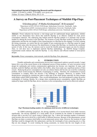
Fig.1 Maximum loading number of a minimum-sized inverter of different technologies
As CMOS technology progresses, the driving capability of an inverter-based clock buffer increases
significantly. The driving capability of a clock buffer can be evaluated by the number of minimum-sized
inverters that it can drive on a given rising or falling time. Fig. 1 shows the maximum number of minimum-
sized inverters that can be driven by a clock buffer in different processes. Because of this phenomenon, several
flip-flops can share a common clock buffer to avoid unnecessary power waste. However, the locations of some
flip-flops would be changed after this replacement, and thus the wirelengths of nets connecting pins to a flip-
flop are also changed. To avoid violating the timing constraints, we restrict that the wire lengths of nets
2. A Survey on post-placement techniques of Multibit flip-flops
12
connecting pins to a flip-flop cannot be longer than specified values after this process. Besides, to guarantee that
a new flipflop can be placed within the desired region, we also need to consider the area capacity of the region.
II. MULTI BIT FLIP-FLOP CONCEPT
In this section, we will introduce multi-bit flip-flop conception. Before that, we will review single-bit
flip-flop. Figure 2 shows an example of single-bit flip-flop. A single-bit flip-flop has two latches (Master latch
and slave latch). The latches need “Clk” and “Clk’ ” signal to perform operations, such as Figure2 shows.
Fig 2: Single-Bit Flip-Flop
In order to have better delay from Clk-> Q, we will regenerate “Clk” from “Clk’”. Hence we will have
two inverters in the clock path. Figure 3 shows an example of merging two 1-bit flip-flops into one 2-bit flip-
flop. Each 1- bit flip-flop contains two inverters, master-latch and slave-latch.
Fig 3: An example of merging two 1-bit flip-flops into one 2-bit flip-flop.
Due to the manufacturing rules, inverters in flip-flops tend to be oversized. As the process technology
advances into smaller geometry nodes like 65nm and beyond, the minimum size of clock drivers can drive more
than one flip-flop.
Merging single-bit flip-flops into one multi-bit flip-flop can avoid duplicate inverters, and lower the total
clock dynamic power consumption. The total area contributing to flip-flops can be reduced as well. By using
multi-bit flip-flop to implement ASIC design, users can enjoy the following benefits:
Lower power consumption by the clock in sequential banked components
Smaller area and delay, due to shared transistors and optimized transistor-level layout.
III. MULTI BIT FLIP-FLOP METHODOLOGY
In the section, we will introduce that how to use Design Compiler and Faraday’s multi-bit flip-flop to
implement ASIC design.
3. A Survey on post-placement techniques of Multibit flip-flops
13
A) The criteria of using multi-bit flip-flop
Multi-bit flip-flop cells are capable of decreasing the power consumption because they have shared
Inverter inside the flip-flop. Meanwhile, they can minimize clock skew at the same time. To obtain these
benefits, the ASIC design must meet the following requirements. The single-bit flip-flops we
want to replace with multi-bit flip-flop must have same clock condition and same set/reset condition.
For post-placement optimization with MBFFs, the previous works separated “MBFF Gen. &
Placement” in Fig. 2(c) into two steps: 1) flip-flop merging, and 2) MBFF placement, based on different design
objectives. During flipflop merging, both tried to minimize total flipflop power consumption, while proposed to
minimize the number of clock sinks (i.e., the total flip-flop number) and net switching power (i.e., the total
weighted wirelength). During MBFF placement, proposed to minimize total wirelength, and considered the
minimization of net switching power.
In this paper, we address the problem of power optimization with MBFFs at the post-placement stage.
We present a new problem formulation for the application of multi-bit flipflops, which simultaneously minimize
total flip-flop power consumption and interconnecting wirelength such that both placement density and timing
slack constraints are satisfied. Based on the problem formulation, we propose a novel postplacement power
optimization flow together with the flip-flop grouping and MBFF placement algorithms to solve the addressed
problem. We formulate the flip-flop grouping problem as the m-clique finding and maximum-independent-set
subproblems. Finally, we introduce the progressive window-based optimization technique to reduce placement
deviation and improve runtime efficiency of our algorithms. Experimental results show that our approach is very
effective in reducing not only flip-flop power consumption but also clock tree and signal net wirelength when
applying multi-bit flip-flops to a design at the post-placement stage.
IV. PROPOSED ALGORITHMS
we propose our algorithms to simultaneously reduce total flipflop power consumption and
interconnecting wirelength at the post-placement stage.First of all, the MBFF consumption of an MBFF cell
divided by its bit number,PfmOnce the MBFF cells in the cell library are sorted, the most power-efficient MBFF
cell is then iteratively extracted. Our algorithms always replace a group of flip-flops with the most power-
efficient MBFF cell during the optimization. After an m-bit flip-flop cell is extracted, two major steps, including
flip-flop grouping and MBFF creation and placement , in the flow will be performed based on the technique of
progressive window based optimization. The first step finds a set of m-bit flip-flop groups in the design while
the second step determines the position of each m-bit flip-flop group and verifies the legality of the position. A
legal position of an m bit flip-flop group means that placing an m-bit flip-flop cell at the position does not
violate any aforementioned design constraints. If the position for an m-bit flip-flop group is legal, an m-bit flip-
flop cell is then created to merge all the flipflops in the m-bit flip-flop group. Otherwise, the flip-flops in the m-
bit flip-flop group cannot be merged.
A. Grouping of Flip-Flops
When grouping a set of flip-flips, the timing slacking constraints between any flip-flop and all its
connected pins should be first considered. According to the timing slacking constraints, we explore all possible
combinations of flip-flop groups for flip-flop merging. Finally, we try to select maximal cells in the cell library
are sorted in ascending order with respect to the flip-flop power consumption per bit non-conflicted flip-flop
groups from all the combinations.
1) Consideration of Timing Slack Constraints:
Based on every flip-flop should be placed in the timing-slack-freeregion which is defined as follows.
Definition 1: A timing-slack-free region (TSFR) of a flipflop is a region where the flip-flop is placed within the
maximum allowable distance from its connected pins such that the timing slack constraints are satisfied.
Fig. 5(a) illustrates the TSFR of f2 which is a tilted rectangular region intersected by the Manhattan rings of p1
and p2. Every point on the Manhattan ring of p1 (p2) has the same Manhattan distance from p1 (p2), which is
equal
4. A Survey on post-placement techniques of Multibit flip-flops
14
Fig. 5. (a) Timing-slack-free region of the flip-flop, f2.
(b) Timing-slackfree regions of the flip-flops, f1, f2, . . . , and f6.
to dmax(p1, f2) (dmax(p2, f2)). Fig. 5(b) further shows all the TSFRs of f1, f2, . . . , and f6 in the same design.
According to the definition of the TSFR, a set of flip-flops can be grouped and replaced by an MBFF if there
exists an intersection region of the TSFRs of all the flip-flops. In Fig. 5(b), f2 and f5 cannot be grouped and
merged by an MBFF since the TSFRs of f2 and f5 are independent without any intersection. On the contrary, f1
and f2 can be grouped and merged by an MBFF because the merged MBFF can be placed in the intersection of
the TSFRs of f1 and f2 such that the timing slack constraint of the merged MBFF is met. Such flip-flop group of
f1 and f2 is called a timing-slack-free group which is defined in the following.
Definition 2: A timing-slack-free group (TSFG) is a flipflop group in which all the flip-flops can be merged by
an MBFF such that the timing slack constraints between the MBFF and all its connected pin are satisfied.
2) Exploration of m-Bit Flip-Flop Groups:
Before exploring the m-bit TSFGs in a design, we construct the TSFR intersection graph which is
defined in Definition 3. Fig. 6(a) shows The TSFR intersection graph representing the relationship of the TSFRs
in Fig. 5(b). The vertices, v1, v2, . . . , v6, represent the six flip-flops, f1, f2, . . . , f6, respectively. If there is an
intersection between the TSFRs of two flip-flops, there is an edge between the corresponding vertices. G(V, E),
where each vertex, vi, corresponds to a flip-flop, fi, in the design, and an edge, eij , between vi and vj exists if
there is an intersection between the TSFRs of fi and fj . Once the TSFR intersection graph of a design is
constructed, we can explore all the m-bit TSFGs in the design by finding all the m-cliques in the TSFR
intersection graph. Each m-clique in The graph corresponds to an m-bit TSFG. The problem of finding all m-
cliques in the graph can be well solved by applying the branch-and-bound and backtracking algorithms using a
search tree as shown in Fig. 6. From the example, we can find all 4-cliques, including {n1, n2, n3, n4} and {n1,
n3, n4, n6}, in the graph. Consequently, the set of 4-bit TSFGs, G4, of the design in Fig. 5(b) contains two
TSFGs, {g41, g42}, where g4
g1 = {f1, f2, f3, f4} and g4
g2 = {f1, f3, f4, f6}.
3) Selection of Flip-Flop Groups:
After exploring theset of m-bit TSFGs of a design denoted by Gm =
{gm1 , gm2 , . . . , gmk}, the next problem is how to select the maximum number of non-conflict m-bit TSFGs
for more
Fig. 6. (a) TSFR intersection graph representing the relationship among the TSFRs in
Fig. 5(b). (b) Branch-and-bound and backtracking algorithms which find all 4-vertex cliques in (a).
5. A Survey on post-placement techniques of Multibit flip-flops
15
Power saving and wirelength reduction. The selection of nonconflict TSFGs can be formulated by
finding the maximum independent set (MIS) in Gm. In the previous example, the MIS in G4 is either {g41} or
{g42} since f1, f3, and f4 belong to both g41 and g42. The independent set of TSFGs is defined as follows.
B. Placement of Flip-Flop Groups
Once the IS of TSFGs is obtained, a proper location for the MBFF corresponding to a TSFG should be
searched.
Fig. 7. (a) Original coordinate system. (b) Transformed coordinate system.
Fig. 8. Example of converting the design in
Fig. 5(b) from the original coordinate system into the transformed coordinate system.
The intersection denotes the valid placement region of the TSFG, g42 = {f1, f3, f4, f6}.
Fig. 9. Placement area of an MBFF with the consideration of interconnecting wire length.
(a) Placement area bounded by the median coordinates of the eight pins.
(b) Enlarged placement area when placing an MBFF in the area in (a) is not feasible.
This sub section, the transformation of the coordinate system is first introduced to improve the
computational efficiency when calculating the intersection of several TSFRs. The placement bins and grids are
then searched for each MBFF corresponding to a TSFG according to the intersection of TSFRs. When finding a
placement bin or a placement grid for each MBFF, we try to minimize the interconnecting wirelength while
satisfying the placement density constraint.
1) Transformation of Coordinate System:
According to Definitions 1 and 2, the MBFF corresponding to a TSFG should be placed within the
intersection of the TSFRs of all the flip-flops in the TSFG. Since all the TSFRs are tilted in 45° with respect to
the placement coordinate system, the intersection of the TSFRs is also tilted in 45°. To efficiently calculated the
coordinates of the intersection from the coordinates of the TSFRs, we transform the coordinate system based on
the transfer functions defined in (4). The difference between the original and the transformed coordinate systems
6. A Survey on post-placement techniques of Multibit flip-flops
16
is demonstrated in Fig. 7. Both coordinate systems can be transformed back and forth based on the transfer and
inverse transfer functions in
_Xtrans = Xorig − Yorig
Ytrans = Yorig + Xorig
_
Xorig = (Xtrans + Ytrans)/2
Yorig = (Ytrans − Xtrans)/2.
Fig. 8 further shows an example of converting the design in Fig. 5(b) into the transformed coordinate system.
After the transformation, all the tilted rectangular regions of the TSFRs become non-tilted. Consequently, it
becomes much
Fig. 10. Placement area of an MBFF with the consideration of interconnecting wirelength.
(a) Placement area bounded by the median coordinates of the eight pins. (b) Enlarged placement area
when placing an MBFF in the area in (a) is not feasible
Easier to calculate the coordinates of the intersection of the TSFRs of all flip-flops in the TSFG, g42 = {f1, f3,
f4,, f6}. Once the coordinates of the intersection region in Fig. 8 are calculated in the transformed coordinate
system, they should be transformed back to the original coordinate system such that the coordinates of the tilted
rectangular placement region in the original coordinate system can be obtained.
2) Consideration of Placement Density:
To find a legal placement for an MBFF corresponding to a TSFG within the tilted rectangular
placement region, or the TSFR of the MBFF, only the placement bins covered by the tilted rectangular
placement region should be considered. To collect all the placement bins, the bins intersected by each boundary
of the tilted rectangular placement region should be first identified as shown in Fig. 9(a) and (b). The bins
surrounded by these intersected bins can be found and collected accordingly. To better consider the placement
density during MBFF placement, the bin with the lowest placement density is chosen to accommodate the
MBFF corresponding to a TSFG. If there is no valid placement grid within the bin, the bin with the second
lowest placement density is then chosen. The grid searching process is repeated until a valid placement grid for
the MBFF is found.
3) Consideration of Interconnecting Wire length:
In addition to considering the placement densities of the bins within the TSFR of an MBFF
corresponding to a TSFG, it is also required to minimize the interconnecting wirelength when placing the MBFF.
To find a position for the MBFF with shorter wirelength, the area bounded by the median coordinates of all pins
connected to the MBFF is first considered as shown in Fig. 10(a). In this example, the median coordinates of the
eight pins are xp4 , xp5 , yp4 , and yp8 in both axes. Once the area bounded by the median coordinates of all
pins is obtained, a grid-searching process is performed to find a valid placement grid. During the grid-searching
process, the bin with the lowest placement density, which contains grids inside the TSFR and the bounded area
of the median coordinates of all pins, is first chosen. For example, in Fig. 11(a), the bin, b22, is
7. A Survey on post-placement techniques of Multibit flip-flops
17
Fig. 11. Example of finding valid placement grids during grid-searching process.
(a) Bins containing placement grids inside both the TSFR of the MBFF and the area bounded by the
median coordinates of all pins connected to the MBFF. (b) All possible placement grids in the bin, b22.
The one with the lowest placement density. A valid placement grid is then searched among all possible
placement grids in b22 as shown in Fig. 11(b).
If there is no valid placement grid in the bin intersected by both the area bounded by the coordinates of
the pins and the TSFR, or the tilted rectangular placement region, the area bounded by the coordinates of the
pins is enlarged to the next pitch which is the closest one from the current pitches. In Fig. 10(b), yp1 is the
closest pitch from yp8 compared with all the other neighboring pitches. The enlarged area for wirelength
minimization is then surrounded by xp4 , xp5 , yp4 , and yp1 . The process is continued until a valid placement
grid for the MBFF is found.
V. CONCLUSION
In this paper, we presented a new problem formulation of post-placement optimization with MBFFs to
optimize the power consumption of the clock network. Based on the problem formulation, we proposed flip-flop
grouping and MBFF placement algorithms to simultaneously minimize flip-flop power consumption and
interconnecting wirelength such that both placement density and timing slack constraints are satisfied. Using
Multi-Bit Flip-flop in combination with gated tree drive is an effective and efficient implementation
methodology to reduce the power consumption by merging single-bit flip-flop. In this paper, we have
implemented design with XILINX Design Compiler and Faraday’s multi-bit flip-flop.
Experimental results indicate that multi-bit flip-flop is very effective and efficient method in lower-
power designs. We will use this methodology to implement real ASIC project in the future
REFERENCES
[1]. Cheon.Y, P.H. Ho, A.B. Kahng, S. Reda, andQ. Wang. Power-aware placement. In Design Automation
Conference, pages 227–232, 2008.
[2]. Donno. M, A. Ivaldi, L. Benini, and E. Macii. Clock-tree power optimization based on RTL clock-
gating. In Design Automation Conference, pages 622–627, 2003.
[3]. Gronowski.P, W. J. Bowhill, R. P. Preston, M. K. Gowan, and R. L.Allmon, “High-performance
microprocessor design,” IEEE J. Solid- StateCircuits, vol. 33, no. 5, pp. 676–686, May 1998
[4]. GaneshBabu .C and P.T.Vanathi, “Performance Analysis of Voice Activity Detection Algorithm
for Robust Speech Recognition System under Different Noisy Environment”, Journal of Scientific &
Industrial Research, Vol.69, PP.515-522, July 2010.
[5]. Hou.W, D. Liu, and P.H. Ho. Automatic register banking for low-power clock trees. In International
Symposium on Quality Electronic Design, pages 647–652, 2009.
[6]. Liu.D and C. Svensson, “Power consumption estimation in CMOS VLSI chips,” IEEE J. Solid-State
Circuits, vol. 29, no. 6, pp. 663–670, Jun. 1994.
[7]. Lalith Kumar.T and R.SundarRajan, “Speech Enhancement using Adaptive Filters”, VSRD-JJEEE,
Vol.2 (2), PP.92-99, 2012.
[8]. Lua.Y, C.N. Sze, X. Hong, Q. Zhou, Y. Cai,L. Huang, and J. Hu. Navigating registers in placement for
clock network minimization. In Design Automation Conference, pages 176–181, 2005.
[9]. Naik.S and R. Chandel. Design of a low power flip-flop using cmos deep sub micron technology. In
International Conference on Recent Trends in Information, Telecommunication and Computing, pages
253–256, 2010.
[10]. Poblinger.G, “Computationally Efficient Speech Enhancement by Spectral Minima Tracking in
Subbands”, Proc. Euro Speech 2, PP.1513-1516, 1995.
8. A Survey on post-placement techniques of Multibit flip-flops
18
[11]. Seyedi A.S, S.H. Rasouli, A. Amirabadi, and A. Afzali-Kusha. Low power low leakage clock gated
static pulsed flip-flop. In IEEE International Symposium on Circuits and Systems, pages 3658–3611,
2006.
[12]. Stan.M.R and W. P. Burleson, “Coding a terminated bus for low power,” in Proc. 5th
GLSVLSI, 1995,
pp. 70–73.
[13]. Stan.M.R and W. P. Burleson, “Bus-invert coding for low-power I/O,” IEEE Trans. Very Large Scale
Integr . (VLSI) Syst. , vol. 3, no. 1, pp.49– 58, Mar. 1995.
[14]. SundarRajan .R and C.L.Philipos, “A Noise Estimation Algorithm for Highly Non-stationary
environments,” speech communication, Vol.48, PP.220-231, 2006.
[15]. Teng .S.K and N. Soin. Low power clock gates optimization for clock tree distribution. In International
Symposium on Quality Electronic Design, pages 488–492, 2010.