SlideShare une entreprise Scribd logo
1  sur  4
Télécharger pour lire hors ligne
The MultiView 2000™
F o r m e r l y       T h e      N S O M / S P M - 2 0 0 0 ™
The First Tip and Sample Scanning Probe Microscope


                                                         ZE
                                                    AL SI
                                                ACTU


Using Two Award Winning Nanonics 3D Micro/Nano Flat Scanners™

• Top plate tip scanner

• Bottom plate sample
  scanner

• Unobstructed optical axis

• Transparent integration with
  any optical microscope,
  including dual microscopes

• Complete freedom of
  optical microscope nose
  piece rotation

• Odd size and large samples
  including hanging samples
  (shown inside)

• Confocal imaging provided
Mechanical Design & Scanning
                                           • Double the z scanning breakthrough achieved with one 3D Flat Scanner™ in
                                             the MultiView 1000™
                                           • Up to 0.120 mm z scanning for ease of approach
                                           • Samples with surface roughness from nanometers to more than one hundred microns
                                           • Hundreds of microns deep imaging with Nanonics Deep Trench™ probes
                                             and 3D Flat Scanners™
                                           • Complete integration with confocal microscopic 3D optical sectioning
                                           • Laser tweezers applications
                                           • Roughly scan samples in x-y over millimeters
                                           • Double the conventional x-y fine motion with two scanning stages - one for
                                             tip and one for sample
                                           • Extreme compactness and closed loop mechanical design for sample stability
                                           • Noise floor < 1nm
MultiView 2000™ Tip Mount                  • Flexible mounting geometries for all near-field optical elements


                                           Breakthrough in Tuning Fork Feedback
                                           • High resonance frequencies
                                           • High Q factors
                                           Tuning forks were pioneered in scanned probe microscopy by K. Karrai and M.
                                           Haines US Patent Number 5,641,896. The work of Karrai and coworkers was
                                           patented for straight near-field optical/AFM elements with highly restricted
                                           geometries of tip attachment and movement. Nanonics extends this technology
                            The Nanonics
                            Proprietary    in two directions: First, the use of proprietary, simple, mounting techniques that
                            Tip Mount      maintain resonance frequencies and Q factors and resolve problems with tuning
                            Viewed from    fork feedback, as noted previously [D. N. Davydov, K. B. Shelimov, T. L. Haslett
                            the Tip Side   and M. Moskovits, Appl. Phys. Lett. 75, 1796 (1999)]; and second, applying these
                                           mounting techniques to cantilevered near-field optical and AFM elements to
                                           provide performance at the limits attainable with scanned probe techniques.


                                           Tip Scanning
                                           Waveguide characterization highlights the utility of having tip and sample scanning
                                           available in a single system. The distribution of light emanating from the edge
                                           of a waveguide can be best imaged by collection mode tip scanning. In this case,
                                           the light is injected into the bottom of the waveguide through an inverted microscope
                                           objective or an input fiber. The geometry of the light source and waveguide must
                                           be kept stationary throughout the measurement, and sample scanning would
                                           disturb the injection of light into the waveguide. Thus, tip scanning collection
                                           mode is preferred in this case and in similar experiments.

                                           Using an on-line optical microscope allows simultaneous viewing of the edge of
                                           a hanging planar waveguide and the NSOM/AFM cantilevered tip as it is positioned
                                           to inject light into the waveguide (top left image). The waveguide is hung on
                                           the bottom plate of the sample scanner while the tip is mounted on the top plate,
                                           the tip scanner (bottom left image).
Sample Scanning
Many experiments are performed best using sample scanning.
For example, one might want to monitor, with ultra high resolution,
index of refraction variations along the edge of the waveguide together
with AFM topography. Light emitted from the NSOM tip and reflected
off the edge of a waveguide is collected by a high numerical aperture
(NA) microscope objective. In such an optical measurement, tip
scanning relative to a high NA objective destroys the axial symmetry
of the optical system and can result in image artifacts. Tip artifacts
have to be avoided to reach the ultimate in these super resolution
reflection measurements of index of refraction that can monitor
alterations of <1/1000.

The MultiView 2000™ Series also includes the LT Low Temperature
systems that Nanonics provides.                                           Soft Sample Imaging of a Fibril
                                                                          of Associated Protein Molecules
The MultiView 2000™ Series builds on the standards of modularity,
flexibility, and full system performance that were established by the
MultiView 1000™. Present owners of a Nanonics MultiView 1000™
can upgrade to the Nanonics MultiView 2000™ Series.


The MultiView 2000™ L (Large Samples)
• Integrate Alpha Step, AFM, and optical information
• Tip scanning
• Large sample stage
• Customer specified stage sizes and accuracy


The MultiView 2000™ C (Confocal Imaging)
• Tip scanning
• Add to any existing optical microscope, including UV confocal
  microscopes
• On-line viewing with lens and tip for imaging and callibration
• Resolve optical image and AFM registration in semiconductor
  applications
• Ultra-high resolution thin film measurements


Accessories for liquid and electrochemical cells, odd-shaped
sample mounts, and environmental control systems
With the MultiView 2000™ Series, Nanonics Imaging has reaffirmed its position
as the complete supplier in this unique interface between scanned probe and
optical microscopy. At Nanonics Imaging, both the optical microscope and the
scanned probe imaging system are given equal importance. No other manufacturer
of scanned probe or optical microscopes can provide for such effective solutions
in both these growing areas of imaging. The result is the ultimate degree of
integration in imaging methodologies.
MultiView 2000™ Technical Specifications
Modes of Operation
Near-field Optical Microscopy   Transmission, reflection, collection, fluorescence
Atomic Force Microscopy         Tuning fork
Feedback Mechanism              Tuning fork (resonance frequency approximately 32 kHz)
Confocal Microscopy             Transmission, reflection, fluorescence


Sample or Tip Scanning
Scanner                         Two piezoelectric flat scanners (both 7 mm thick)
                                Sample scanning or tip scanning
                                Scan Range: 120 µ Z-range, 70 µ XY-range (30 and 10 µ on request)
                                Maximum Load: 75 g
Resolution                      < 5 nm in XY, < 1 nm in Z
Sample Positioning              Inertial piezo motion (6 mm range, accuracy 1 µ)
Maximum Sample Size             16 mm diameter, custom mounts for larger samples available upon request


Probes
NSOM Probes                     Cantilevered or straight, pulled optical fiber probes
AFM Probes                      Cantilevered, pulled glass probes or any commercially available AFM probes
Specialized Probes              Cantilevered probes for electrical or thermal measurements
Custom Probes                   Available upon request


Optics
Viewing/Detection Optics        Free optical access to the sample from top and bottom for optical observation
                                of the sample (all conventional far-field modes of operation are available)
                                and for detection of the NSOM signals with any optical microscope (upright,
                                inverted, dual) or other optics
Detectors                       Photomultiplier Tube (PMT), Avalanche Photodiode Detector (APD), InGaAs
                                Detector for IR, CCD
Lasers                          A large variety of laser systems can be used (UV, VIS, IR)
Video System                    Optional CCD camera


Optical Resolution
Confocal Microscopy             Diffraction limited
Near-field Microscopy           From 50 nm upwards, depending on the aperture size of the NSOM probe used
Controller                      Nanonics/Topaz (Digital Instruments, RHK, Park Scientific and Topometrix
                                controllers can also be used to control the MultiView 2000™ microscope)
Software                        Quartz software for Nanonics/Topaz controller (Win 95/98 and NT)
                                Real time image display, image acquisition (up to 8 channels) and analysis,
                                3D rendering


Options
Environmental Chamber           Control the measurement environment (humidity, gas composition, vacuum)
Electrical Measurements         Options for resistance, thermal measurements
Nanochemical/Gas Delivery       Deliver a chemical via the nanopipette/AFM tip to the sample surface

                                                                                                                Manhat Technology Park, Malcha
                                                                                                                    Jerusalem 91487, Israel
                                                                                                                      Tel: +972-2-6789573
                                                                                                                     Fax: +972-2-6480827
                                                                                                                  US Toll-free: 1-866-220-6828
                                                                                                                      www.nanonics.co.il
                                                                                                                   email: info@nanonics.co.il

Contenu connexe

Tendances

EUV Lithography Final
EUV Lithography FinalEUV Lithography Final
EUV Lithography Final
Ehud Ben Ari
 
Flouroscopic imging
Flouroscopic imgingFlouroscopic imging
Flouroscopic imging
Sahith Reddy
 
Spm And Sicm Lecture
Spm And Sicm LectureSpm And Sicm Lecture
Spm And Sicm Lecture
sschraml
 
Principle Of A F S
Principle Of  A F SPrinciple Of  A F S
Principle Of A F S
guestc5e21a
 
tomography tomography - Presentation Transcript 1. PRINCIPLE OFTOMOGRAPHY...
tomography tomography - Presentation Transcript     1. PRINCIPLE OFTOMOGRAPHY...tomography tomography - Presentation Transcript     1. PRINCIPLE OFTOMOGRAPHY...
tomography tomography - Presentation Transcript 1. PRINCIPLE OFTOMOGRAPHY...
Prem Murti
 
afm by anam rana
afm by anam ranaafm by anam rana
afm by anam rana
PAKISTAN041
 

Tendances (19)

EUV Lithography Final
EUV Lithography FinalEUV Lithography Final
EUV Lithography Final
 
Fluoroscopy presentation1
Fluoroscopy presentation1Fluoroscopy presentation1
Fluoroscopy presentation1
 
Atomic Force Microscope
Atomic Force MicroscopeAtomic Force Microscope
Atomic Force Microscope
 
Atomic Force Microscope: Fundamental Principles
Atomic Force Microscope: Fundamental PrinciplesAtomic Force Microscope: Fundamental Principles
Atomic Force Microscope: Fundamental Principles
 
LLTech Light-CT comparison vs OCT and confocal microscopy
LLTech Light-CT comparison vs OCT and confocal microscopyLLTech Light-CT comparison vs OCT and confocal microscopy
LLTech Light-CT comparison vs OCT and confocal microscopy
 
Viewing and recording the fluoroscopic image
Viewing and recording the fluoroscopic imageViewing and recording the fluoroscopic image
Viewing and recording the fluoroscopic image
 
Flouroscopic imging
Flouroscopic imgingFlouroscopic imging
Flouroscopic imging
 
Flat Panel Digital Fluoroscopy by Akash Das
Flat Panel Digital Fluoroscopy by Akash Das Flat Panel Digital Fluoroscopy by Akash Das
Flat Panel Digital Fluoroscopy by Akash Das
 
Cameras artical11
Cameras artical11Cameras artical11
Cameras artical11
 
Spm And Sicm Lecture
Spm And Sicm LectureSpm And Sicm Lecture
Spm And Sicm Lecture
 
Near field scanning optical microscopy
Near field scanning optical microscopyNear field scanning optical microscopy
Near field scanning optical microscopy
 
Principle Of A F S
Principle Of  A F SPrinciple Of  A F S
Principle Of A F S
 
Applications of atomic force microscope(by kanupriya)
Applications of atomic force microscope(by kanupriya)Applications of atomic force microscope(by kanupriya)
Applications of atomic force microscope(by kanupriya)
 
atomic force microscopy AFM
atomic force microscopy AFMatomic force microscopy AFM
atomic force microscopy AFM
 
ATOMIC FORCE MICROSCOPE MITHILESH CHOUDHARY
ATOMIC FORCE MICROSCOPE MITHILESH CHOUDHARYATOMIC FORCE MICROSCOPE MITHILESH CHOUDHARY
ATOMIC FORCE MICROSCOPE MITHILESH CHOUDHARY
 
tomography tomography - Presentation Transcript 1. PRINCIPLE OFTOMOGRAPHY...
tomography tomography - Presentation Transcript     1. PRINCIPLE OFTOMOGRAPHY...tomography tomography - Presentation Transcript     1. PRINCIPLE OFTOMOGRAPHY...
tomography tomography - Presentation Transcript 1. PRINCIPLE OFTOMOGRAPHY...
 
Atomic Force Microscopy
Atomic Force MicroscopyAtomic Force Microscopy
Atomic Force Microscopy
 
afm by anam rana
afm by anam ranaafm by anam rana
afm by anam rana
 
Rad 206 p05 Fundamentals of Imaging - Fluoroscopy
Rad 206 p05 Fundamentals of Imaging - FluoroscopyRad 206 p05 Fundamentals of Imaging - Fluoroscopy
Rad 206 p05 Fundamentals of Imaging - Fluoroscopy
 

Similaire à Nanonics - Raman MultiProbe

Samer najjar fiber optic leak detection
Samer najjar   fiber optic leak detectionSamer najjar   fiber optic leak detection
Samer najjar fiber optic leak detection
Ramy Saboungui
 
Hamby-Research-SREU Abstract
Hamby-Research-SREU AbstractHamby-Research-SREU Abstract
Hamby-Research-SREU Abstract
Robert Hamby
 
ETE444-lec2-atomic_scale_characterization_techniques.pdf
ETE444-lec2-atomic_scale_characterization_techniques.pdfETE444-lec2-atomic_scale_characterization_techniques.pdf
ETE444-lec2-atomic_scale_characterization_techniques.pdf
mashiur
 

Similaire à Nanonics - Raman MultiProbe (20)

20120927 台科大 oct原理及在眼科的應用 (1)
20120927 台科大 oct原理及在眼科的應用 (1)20120927 台科大 oct原理及在眼科的應用 (1)
20120927 台科大 oct原理及在眼科的應用 (1)
 
Static force curve activity in nanofluidic channels
Static force curve activity in nanofluidic channelsStatic force curve activity in nanofluidic channels
Static force curve activity in nanofluidic channels
 
Near Field Scattering Optical Microscopy (NSOM)
Near Field Scattering Optical Microscopy (NSOM)Near Field Scattering Optical Microscopy (NSOM)
Near Field Scattering Optical Microscopy (NSOM)
 
Cbct
CbctCbct
Cbct
 
OCT MACULA INTERPRETATION.
OCT MACULA  INTERPRETATION.OCT MACULA  INTERPRETATION.
OCT MACULA INTERPRETATION.
 
Introduction of SG-O CIS / ALS / Light-Sensor Wafer Tester
Introduction of SG-O CIS / ALS / Light-Sensor Wafer TesterIntroduction of SG-O CIS / ALS / Light-Sensor Wafer Tester
Introduction of SG-O CIS / ALS / Light-Sensor Wafer Tester
 
LEXT OLS4100 3D Measuring Laser Microscope
LEXT OLS4100 3D Measuring Laser MicroscopeLEXT OLS4100 3D Measuring Laser Microscope
LEXT OLS4100 3D Measuring Laser Microscope
 
Mar Surf Ws 1 Flyer
Mar Surf Ws 1 FlyerMar Surf Ws 1 Flyer
Mar Surf Ws 1 Flyer
 
Nanophotonic Characterization in the Century of Photonics
Nanophotonic Characterization in the Century of PhotonicsNanophotonic Characterization in the Century of Photonics
Nanophotonic Characterization in the Century of Photonics
 
Measurement techniques in micro machining PDF by badebhau4@gmail.com
Measurement techniques in micro machining PDF by badebhau4@gmail.comMeasurement techniques in micro machining PDF by badebhau4@gmail.com
Measurement techniques in micro machining PDF by badebhau4@gmail.com
 
Samer najjar fiber optic leak detection
Samer najjar   fiber optic leak detectionSamer najjar   fiber optic leak detection
Samer najjar fiber optic leak detection
 
Fully 3D-Integrated Pixel Detectors for X-Rays
Fully 3D-Integrated Pixel Detectors for X-RaysFully 3D-Integrated Pixel Detectors for X-Rays
Fully 3D-Integrated Pixel Detectors for X-Rays
 
UNIT 4.pptx
UNIT 4.pptxUNIT 4.pptx
UNIT 4.pptx
 
AFM and STM (Scanning probe microscopy)
AFM and STM (Scanning probe microscopy)AFM and STM (Scanning probe microscopy)
AFM and STM (Scanning probe microscopy)
 
Fona xdg brochure
Fona xdg brochureFona xdg brochure
Fona xdg brochure
 
Fona XDG
Fona XDGFona XDG
Fona XDG
 
Hamby-Research-SREU Abstract
Hamby-Research-SREU AbstractHamby-Research-SREU Abstract
Hamby-Research-SREU Abstract
 
ETE444-lec2-atomic_scale_characterization_techniques.pdf
ETE444-lec2-atomic_scale_characterization_techniques.pdfETE444-lec2-atomic_scale_characterization_techniques.pdf
ETE444-lec2-atomic_scale_characterization_techniques.pdf
 
Atomic Force Microscope
Atomic Force MicroscopeAtomic Force Microscope
Atomic Force Microscope
 
Cbct
CbctCbct
Cbct
 

Dernier

Russian Call Girls Lucknow Just Call 👉👉7877925207 Top Class Call Girl Service...
Russian Call Girls Lucknow Just Call 👉👉7877925207 Top Class Call Girl Service...Russian Call Girls Lucknow Just Call 👉👉7877925207 Top Class Call Girl Service...
Russian Call Girls Lucknow Just Call 👉👉7877925207 Top Class Call Girl Service...
adilkhan87451
 

Dernier (20)

Russian Call Girls Lucknow Just Call 👉👉7877925207 Top Class Call Girl Service...
Russian Call Girls Lucknow Just Call 👉👉7877925207 Top Class Call Girl Service...Russian Call Girls Lucknow Just Call 👉👉7877925207 Top Class Call Girl Service...
Russian Call Girls Lucknow Just Call 👉👉7877925207 Top Class Call Girl Service...
 
Call Girls Vasai Virar Just Call 9630942363 Top Class Call Girl Service Avail...
Call Girls Vasai Virar Just Call 9630942363 Top Class Call Girl Service Avail...Call Girls Vasai Virar Just Call 9630942363 Top Class Call Girl Service Avail...
Call Girls Vasai Virar Just Call 9630942363 Top Class Call Girl Service Avail...
 
Night 7k to 12k Navi Mumbai Call Girl Photo 👉 BOOK NOW 9833363713 👈 ♀️ night ...
Night 7k to 12k Navi Mumbai Call Girl Photo 👉 BOOK NOW 9833363713 👈 ♀️ night ...Night 7k to 12k Navi Mumbai Call Girl Photo 👉 BOOK NOW 9833363713 👈 ♀️ night ...
Night 7k to 12k Navi Mumbai Call Girl Photo 👉 BOOK NOW 9833363713 👈 ♀️ night ...
 
Pondicherry Call Girls Book Now 9630942363 Top Class Pondicherry Escort Servi...
Pondicherry Call Girls Book Now 9630942363 Top Class Pondicherry Escort Servi...Pondicherry Call Girls Book Now 9630942363 Top Class Pondicherry Escort Servi...
Pondicherry Call Girls Book Now 9630942363 Top Class Pondicherry Escort Servi...
 
(Low Rate RASHMI ) Rate Of Call Girls Jaipur ❣ 8445551418 ❣ Elite Models & Ce...
(Low Rate RASHMI ) Rate Of Call Girls Jaipur ❣ 8445551418 ❣ Elite Models & Ce...(Low Rate RASHMI ) Rate Of Call Girls Jaipur ❣ 8445551418 ❣ Elite Models & Ce...
(Low Rate RASHMI ) Rate Of Call Girls Jaipur ❣ 8445551418 ❣ Elite Models & Ce...
 
Saket * Call Girls in Delhi - Phone 9711199012 Escorts Service at 6k to 50k a...
Saket * Call Girls in Delhi - Phone 9711199012 Escorts Service at 6k to 50k a...Saket * Call Girls in Delhi - Phone 9711199012 Escorts Service at 6k to 50k a...
Saket * Call Girls in Delhi - Phone 9711199012 Escorts Service at 6k to 50k a...
 
💕SONAM KUMAR💕Premium Call Girls Jaipur ↘️9257276172 ↙️One Night Stand With Lo...
💕SONAM KUMAR💕Premium Call Girls Jaipur ↘️9257276172 ↙️One Night Stand With Lo...💕SONAM KUMAR💕Premium Call Girls Jaipur ↘️9257276172 ↙️One Night Stand With Lo...
💕SONAM KUMAR💕Premium Call Girls Jaipur ↘️9257276172 ↙️One Night Stand With Lo...
 
Model Call Girls In Chennai WhatsApp Booking 7427069034 call girl service 24 ...
Model Call Girls In Chennai WhatsApp Booking 7427069034 call girl service 24 ...Model Call Girls In Chennai WhatsApp Booking 7427069034 call girl service 24 ...
Model Call Girls In Chennai WhatsApp Booking 7427069034 call girl service 24 ...
 
Call Girls Hosur Just Call 9630942363 Top Class Call Girl Service Available
Call Girls Hosur Just Call 9630942363 Top Class Call Girl Service AvailableCall Girls Hosur Just Call 9630942363 Top Class Call Girl Service Available
Call Girls Hosur Just Call 9630942363 Top Class Call Girl Service Available
 
Premium Call Girls In Jaipur {8445551418} ❤️VVIP SEEMA Call Girl in Jaipur Ra...
Premium Call Girls In Jaipur {8445551418} ❤️VVIP SEEMA Call Girl in Jaipur Ra...Premium Call Girls In Jaipur {8445551418} ❤️VVIP SEEMA Call Girl in Jaipur Ra...
Premium Call Girls In Jaipur {8445551418} ❤️VVIP SEEMA Call Girl in Jaipur Ra...
 
Independent Call Girls In Jaipur { 8445551418 } ✔ ANIKA MEHTA ✔ Get High Prof...
Independent Call Girls In Jaipur { 8445551418 } ✔ ANIKA MEHTA ✔ Get High Prof...Independent Call Girls In Jaipur { 8445551418 } ✔ ANIKA MEHTA ✔ Get High Prof...
Independent Call Girls In Jaipur { 8445551418 } ✔ ANIKA MEHTA ✔ Get High Prof...
 
Call Girls Ahmedabad Just Call 9630942363 Top Class Call Girl Service Available
Call Girls Ahmedabad Just Call 9630942363 Top Class Call Girl Service AvailableCall Girls Ahmedabad Just Call 9630942363 Top Class Call Girl Service Available
Call Girls Ahmedabad Just Call 9630942363 Top Class Call Girl Service Available
 
Independent Call Girls Service Mohali Sector 116 | 6367187148 | Call Girl Ser...
Independent Call Girls Service Mohali Sector 116 | 6367187148 | Call Girl Ser...Independent Call Girls Service Mohali Sector 116 | 6367187148 | Call Girl Ser...
Independent Call Girls Service Mohali Sector 116 | 6367187148 | Call Girl Ser...
 
All Time Service Available Call Girls Marine Drive 📳 9820252231 For 18+ VIP C...
All Time Service Available Call Girls Marine Drive 📳 9820252231 For 18+ VIP C...All Time Service Available Call Girls Marine Drive 📳 9820252231 For 18+ VIP C...
All Time Service Available Call Girls Marine Drive 📳 9820252231 For 18+ VIP C...
 
VIP Hyderabad Call Girls Bahadurpally 7877925207 ₹5000 To 25K With AC Room 💚😋
VIP Hyderabad Call Girls Bahadurpally 7877925207 ₹5000 To 25K With AC Room 💚😋VIP Hyderabad Call Girls Bahadurpally 7877925207 ₹5000 To 25K With AC Room 💚😋
VIP Hyderabad Call Girls Bahadurpally 7877925207 ₹5000 To 25K With AC Room 💚😋
 
Premium Bangalore Call Girls Jigani Dail 6378878445 Escort Service For Hot Ma...
Premium Bangalore Call Girls Jigani Dail 6378878445 Escort Service For Hot Ma...Premium Bangalore Call Girls Jigani Dail 6378878445 Escort Service For Hot Ma...
Premium Bangalore Call Girls Jigani Dail 6378878445 Escort Service For Hot Ma...
 
Manyata Tech Park ( Call Girls ) Bangalore ✔ 6297143586 ✔ Hot Model With Sexy...
Manyata Tech Park ( Call Girls ) Bangalore ✔ 6297143586 ✔ Hot Model With Sexy...Manyata Tech Park ( Call Girls ) Bangalore ✔ 6297143586 ✔ Hot Model With Sexy...
Manyata Tech Park ( Call Girls ) Bangalore ✔ 6297143586 ✔ Hot Model With Sexy...
 
Most Beautiful Call Girl in Bangalore Contact on Whatsapp
Most Beautiful Call Girl in Bangalore Contact on WhatsappMost Beautiful Call Girl in Bangalore Contact on Whatsapp
Most Beautiful Call Girl in Bangalore Contact on Whatsapp
 
Call Girls Madurai Just Call 9630942363 Top Class Call Girl Service Available
Call Girls Madurai Just Call 9630942363 Top Class Call Girl Service AvailableCall Girls Madurai Just Call 9630942363 Top Class Call Girl Service Available
Call Girls Madurai Just Call 9630942363 Top Class Call Girl Service Available
 
Andheri East ) Call Girls in Mumbai Phone No 9004268417 Elite Escort Service ...
Andheri East ) Call Girls in Mumbai Phone No 9004268417 Elite Escort Service ...Andheri East ) Call Girls in Mumbai Phone No 9004268417 Elite Escort Service ...
Andheri East ) Call Girls in Mumbai Phone No 9004268417 Elite Escort Service ...
 

Nanonics - Raman MultiProbe

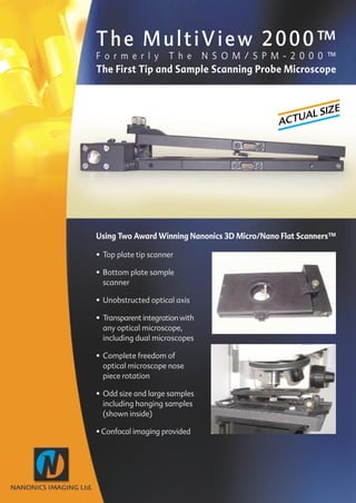
  • 1. The MultiView 2000™ F o r m e r l y T h e N S O M / S P M - 2 0 0 0 ™ The First Tip and Sample Scanning Probe Microscope ZE AL SI ACTU Using Two Award Winning Nanonics 3D Micro/Nano Flat Scanners™ • Top plate tip scanner • Bottom plate sample scanner • Unobstructed optical axis • Transparent integration with any optical microscope, including dual microscopes • Complete freedom of optical microscope nose piece rotation • Odd size and large samples including hanging samples (shown inside) • Confocal imaging provided
  • 2. Mechanical Design & Scanning • Double the z scanning breakthrough achieved with one 3D Flat Scanner™ in the MultiView 1000™ • Up to 0.120 mm z scanning for ease of approach • Samples with surface roughness from nanometers to more than one hundred microns • Hundreds of microns deep imaging with Nanonics Deep Trench™ probes and 3D Flat Scanners™ • Complete integration with confocal microscopic 3D optical sectioning • Laser tweezers applications • Roughly scan samples in x-y over millimeters • Double the conventional x-y fine motion with two scanning stages - one for tip and one for sample • Extreme compactness and closed loop mechanical design for sample stability • Noise floor < 1nm MultiView 2000™ Tip Mount • Flexible mounting geometries for all near-field optical elements Breakthrough in Tuning Fork Feedback • High resonance frequencies • High Q factors Tuning forks were pioneered in scanned probe microscopy by K. Karrai and M. Haines US Patent Number 5,641,896. The work of Karrai and coworkers was patented for straight near-field optical/AFM elements with highly restricted geometries of tip attachment and movement. Nanonics extends this technology The Nanonics Proprietary in two directions: First, the use of proprietary, simple, mounting techniques that Tip Mount maintain resonance frequencies and Q factors and resolve problems with tuning Viewed from fork feedback, as noted previously [D. N. Davydov, K. B. Shelimov, T. L. Haslett the Tip Side and M. Moskovits, Appl. Phys. Lett. 75, 1796 (1999)]; and second, applying these mounting techniques to cantilevered near-field optical and AFM elements to provide performance at the limits attainable with scanned probe techniques. Tip Scanning Waveguide characterization highlights the utility of having tip and sample scanning available in a single system. The distribution of light emanating from the edge of a waveguide can be best imaged by collection mode tip scanning. In this case, the light is injected into the bottom of the waveguide through an inverted microscope objective or an input fiber. The geometry of the light source and waveguide must be kept stationary throughout the measurement, and sample scanning would disturb the injection of light into the waveguide. Thus, tip scanning collection mode is preferred in this case and in similar experiments. Using an on-line optical microscope allows simultaneous viewing of the edge of a hanging planar waveguide and the NSOM/AFM cantilevered tip as it is positioned to inject light into the waveguide (top left image). The waveguide is hung on the bottom plate of the sample scanner while the tip is mounted on the top plate, the tip scanner (bottom left image).
  • 3. Sample Scanning Many experiments are performed best using sample scanning. For example, one might want to monitor, with ultra high resolution, index of refraction variations along the edge of the waveguide together with AFM topography. Light emitted from the NSOM tip and reflected off the edge of a waveguide is collected by a high numerical aperture (NA) microscope objective. In such an optical measurement, tip scanning relative to a high NA objective destroys the axial symmetry of the optical system and can result in image artifacts. Tip artifacts have to be avoided to reach the ultimate in these super resolution reflection measurements of index of refraction that can monitor alterations of <1/1000. The MultiView 2000™ Series also includes the LT Low Temperature systems that Nanonics provides. Soft Sample Imaging of a Fibril of Associated Protein Molecules The MultiView 2000™ Series builds on the standards of modularity, flexibility, and full system performance that were established by the MultiView 1000™. Present owners of a Nanonics MultiView 1000™ can upgrade to the Nanonics MultiView 2000™ Series. The MultiView 2000™ L (Large Samples) • Integrate Alpha Step, AFM, and optical information • Tip scanning • Large sample stage • Customer specified stage sizes and accuracy The MultiView 2000™ C (Confocal Imaging) • Tip scanning • Add to any existing optical microscope, including UV confocal microscopes • On-line viewing with lens and tip for imaging and callibration • Resolve optical image and AFM registration in semiconductor applications • Ultra-high resolution thin film measurements Accessories for liquid and electrochemical cells, odd-shaped sample mounts, and environmental control systems With the MultiView 2000™ Series, Nanonics Imaging has reaffirmed its position as the complete supplier in this unique interface between scanned probe and optical microscopy. At Nanonics Imaging, both the optical microscope and the scanned probe imaging system are given equal importance. No other manufacturer of scanned probe or optical microscopes can provide for such effective solutions in both these growing areas of imaging. The result is the ultimate degree of integration in imaging methodologies.
  • 4. MultiView 2000™ Technical Specifications Modes of Operation Near-field Optical Microscopy Transmission, reflection, collection, fluorescence Atomic Force Microscopy Tuning fork Feedback Mechanism Tuning fork (resonance frequency approximately 32 kHz) Confocal Microscopy Transmission, reflection, fluorescence Sample or Tip Scanning Scanner Two piezoelectric flat scanners (both 7 mm thick) Sample scanning or tip scanning Scan Range: 120 µ Z-range, 70 µ XY-range (30 and 10 µ on request) Maximum Load: 75 g Resolution < 5 nm in XY, < 1 nm in Z Sample Positioning Inertial piezo motion (6 mm range, accuracy 1 µ) Maximum Sample Size 16 mm diameter, custom mounts for larger samples available upon request Probes NSOM Probes Cantilevered or straight, pulled optical fiber probes AFM Probes Cantilevered, pulled glass probes or any commercially available AFM probes Specialized Probes Cantilevered probes for electrical or thermal measurements Custom Probes Available upon request Optics Viewing/Detection Optics Free optical access to the sample from top and bottom for optical observation of the sample (all conventional far-field modes of operation are available) and for detection of the NSOM signals with any optical microscope (upright, inverted, dual) or other optics Detectors Photomultiplier Tube (PMT), Avalanche Photodiode Detector (APD), InGaAs Detector for IR, CCD Lasers A large variety of laser systems can be used (UV, VIS, IR) Video System Optional CCD camera Optical Resolution Confocal Microscopy Diffraction limited Near-field Microscopy From 50 nm upwards, depending on the aperture size of the NSOM probe used Controller Nanonics/Topaz (Digital Instruments, RHK, Park Scientific and Topometrix controllers can also be used to control the MultiView 2000™ microscope) Software Quartz software for Nanonics/Topaz controller (Win 95/98 and NT) Real time image display, image acquisition (up to 8 channels) and analysis, 3D rendering Options Environmental Chamber Control the measurement environment (humidity, gas composition, vacuum) Electrical Measurements Options for resistance, thermal measurements Nanochemical/Gas Delivery Deliver a chemical via the nanopipette/AFM tip to the sample surface Manhat Technology Park, Malcha Jerusalem 91487, Israel Tel: +972-2-6789573 Fax: +972-2-6480827 US Toll-free: 1-866-220-6828 www.nanonics.co.il email: info@nanonics.co.il