1. L293B
L293E
PUSH-PULL FOUR CHANNEL DRIVERS
.
. OUTPUT CURRENT 1A PER CHANNEL
PEAK OUTPUT CURRENT 2A PER CHANNEL
.
.
(non repetitive)
INHIBIT FACILITY
.
.
HIGH NOISE IMMUNITY
SEPARATE LOGIC SUPPLY
OVERTEMPERATURE PROTECTION
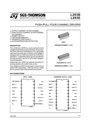
DIP16
DESCRIPTION ORDERING NUMBER : L293B
The L293B and L293E are quad push-pull drivers
capableof delivering output currents to 1A per chan-
nel. Each channel is controlledby a TTL-compatible
logic input and each pair of drivers (a full bridge) is
equipped with an inhibit input which turns off all four
transistors. A separate supply input is provided for
the logic so that it may be run off a lower voltage to
reduce dissipation.
Additionally, the L293E has external connection of POWERDIP (16 + 2+ 2)
sensing resistors, for switchmode control.
The L293Band L293E are package in 16 and 20-pin ORDERING NUMBER : L293E
plastic DIPs respectively ; both use the four center
pins to conduct heat to the printed circuit board.
PIN CONNECTIONS
DIP16 - L293B POWERDIP (16+2+2) - L293E
April 1993 1/12
3. L293B - L293E
SCHEMATIC DIAGRAM
(*) In the L293 these points are not externally available. They are internally connected to the ground (substrate).
O Pins of L293 () Pins of L293E.
3/12
4. L293B - L293E
ABSOLUTE MAXIMUM RATINGS
Symbol Parameter Value Unit
Vs Supply Voltage 36 V
Vss Logic Supply Voltage 36 V
Vi Input Voltage 7 V
Vinh Inhibit Voltage 7 V
Iout Peak Output Current (non repetitive t = 5ms) 2 A
o
Ptot Total Power Dissipation at Tground-pins = 80 C 5 W
o
Tstg, Tj Storage and Junction Temperature –40 to +150 C
THERMAL DATA
Symbol Parameter Value Unit
o
Rth j-case Thermal Resistance Junction-case Max. 14 C/W
o
R th j-amb Thermal Resistance Junction-ambient Max. 80 C/W
ELECTRICAL CHARACTERISTICS
For each channel, VS = 24V, VSS = 5V, Tamb = 25oC, unless otherwise specified
Symbol Parameter Test Conditions Min. TYp. Max. Unit
Vs Supply Voltage Vss 36 V
Vss Logic Supply Voltage 4.5 36 V
Is Total Quiescent Supply Current Vi = L Io = 0 Vinh = H 2 6 mA
Vi = H Io = 0 Vinh = H 16 24
Vinh = L 4
Iss Total Quiescent Logic Supply Current Vi = L Io = 0 Vinh = H 44 60 mA
Vi = H Io = 0 Vinh = H 16 22
Vinh = L 16 24
ViL Input Low Voltage -03. 1.5 V
ViH Input High Voltage VSS ≤ 7V 2.3 Vss V
Vss > 7V 2.3 7
IiL Low Voltage Input Current Vil = 1.5V -10 µA
IiH High Voltage Input Current 2.3V ≤ VIH ≤ Vss - 0.6V 30 100 µA
VinhL Inhibit Low Voltage -0.3 1.5 V
VinhH Inhibit High Voltage VSS ≤ 7V 2.3 Vss V
Vss > 7V 2.3 7
IinhL Low Voltage Inhibit Current VinhL = 1.5V -30 -100 µA
IinhH High Voltage Inhibit Current 2.3V ≤ Vinh H ≤ Vss - 0.6V ±10 µA
VCEsatH Source Output Saturation Voltage Io = -1A 1.4 1.8 V
VCEsatL Sink Output Saturation Voltage Io = 1A 1.2 1.8 V
VSENS Sensing Voltage (pins 4, 7, 14, 17) (**) 2 V
tr Rise Time 0.1 to 0.9 Vo (*) 250 ns
tf Fall Time 0.9 to 0.1 Vo (*) 250 ns
ton Turn-on Delay 0.5 Vi to 0.5 Vo (*) 750 ns
toff Turn-off Delay 0.5 Vi to 0.5 Vo (*) 200 ns
* See figure 1
** Referred to L293E
TRUTH TABLE
Vi (each channel) Vo Vinh (∞)
H H H
L L H
o
H X() L
o
L X() L
(*) High output impedance
(**) Relative to the considerate channel
4/12
5. L293B - L293E
Figure 1 : Switching Timers
Figure 2 : Saturation voltage versus Output Figure 3 : Source Saturation Voltage versus
Current Ambient Temperature
Figure 4 : Sink Saturation Voltage versus Figure 5 : Quiescent Logic Supply Current
Ambient Temperature versus Logic Supply Voltage
5/12
6. L293B - L293E
Figure 6 : Output Voltage versus Figure 7 : Output Voltage versus
Input Voltage Inhibit Voltage
APPLICATION INFORMATION
Figure 8 : DC Motor Controls Figure 9 : Bidirectional DC Motor Control
(with connection to ground and
to the supply voltage)
Vinh A M1 B M2 Inputs Function
H H Fast Motor Stop H Run Vinh = H C= H;D=L Turn Right
H L Run L Fast Motor Stop C = L; D =H Turn Left
L X Free Running X Free Running C=D Fast Motor Stop
Motor Stop Motor Stop
Vinh = L C = X; D =X Free Running
L = Low H = High X = Don’t Care Motor Stop
L = Low H = High X = Don’t Care
6/12
8. L293B - L293E
Figure 11 :Stepping Motor Driver with Phase Current Control and Short Circuit Protection
8/12
9. L293B - L293E
MOUNTING INSTRUCTIONS During soldering the pins temperature must not ex-
The Rth j-amb of the L293B and the L293E can be re- ceed 260oC and the soldering time must not be
duced by soldering the GND pins to a suitable cop- longer than 12 seconds.
per area of the printed circuit board as shown in fig- The external heatsink or printed circuit copper area
ure 12 or to an external heatsink (figure 13). must be connected to electrical ground.
Figure 12 :Example of P.C. Board Copper Figure 13 :External Heatsink Mounting Ex-
Area which is Used as Heatsink ample (Rth = 30oC/W)
9/12
10. L293B - L293E
DIP16 PACKAGE MECHANICAL DATA
Millimeters Inches
Dimensions
Min. Typ. Max. Min. Typ. Max.
a1 0.51 0.020
B 0.77 1.65 0.030 0.065
b 0.5 0.020
b1 0.25 0.010
DIP16PW.TBL
D 20 0.787
E 8.5 0.335
e 2.54 0.100
e3 17.78 0.700
F 7.1 0.280
i 5.1 0.201
L 3.3 0.130
Z 1.27 0.050
a1
I
b1
L
b B e E
Z
e3
D
PMDIP16W.EPS
16 9
F
1 8
10/12
11. L293B - L293E
POWERDIP (16+2+2) PACKAGE MECHANICAL DATA
Millimeters Inches
Dimensions
Min. Typ. Max. Min. Typ. Max.
a1 0.51 0.020
B 0.85 1.4 0.033 0.055
b 0.5 0.020
b1 0.38 0.5 0.015 0.020
DIP20PW.TBL
D 24.8 0.976
E 8.8 0.346
e 2.54 0.100
e3 22.86 0.900
F 7.1 0.280
i 5.1 0.201
L 3.3 0.130
Z 1.27 0.050
a1
I
b1
L
b B e E
Z
e3 Z
D
PMDIP20WEPS
20 11
F
1 10
11/12