
Recommandé
Contenu connexe
Tendances
Tendances (20)
Similaire à MEI 2015 Technology Roadmap
Similaire à MEI 2015 Technology Roadmap (20)
Dernier
Dernier (20)
MEI 2015 Technology Roadmap
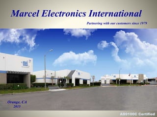
- 1. Marcel Electronics International Orange, CA 2015 Partnering with our customers since 1979
- 2. 42,000 Sq. Ft. Facility Privately Owned 150 Employees AS9100C ISO-9001:2008 IPC-6012 Class 3 & 3A IPC-6016 (HDI) IPC-6018 (RF) ITAR Small Business Listing
- 3. Communications RF MicrowaveSatellite Weapons Systems Defense and Aerospace Lockheed Martin BAE Electronics Exelis Inc Ball Aerospace Sandia Labs L-3 Communications DRS Cubic Defense MIT Lincoln Laboratory Boeing Cobham Draper Labs General Dynamics Harris Corp. Defense & Aerospace represents 53% MEI’s revenues
- 4. Commercial Segments Commercial represents 47% of MEI’s revenues Wireless ATE Medical Storage Networking Broadcom LSI Analog Devices Motorola Texas Instruments General Electric Micron Intel Maxim Fujitsu Teradyne Cisco
- 5. Phase 2 • 25:1 Aspect Ratio • Precision Back Drilling • Panasonic Laminates • Copper Filled µVias • Heat Sink Application • Ticer Resistor Material Phase 3 • RF Focused • Multiple “Z Wrap” • Teflon/Duroid Materials • 10 Stacked u Vias • .004 Mech. Drill thru .093 • IST Testing Phase 4 • Z-Axis Interconnect Ormet/Rogers 2929 • Zeta Laminates • High Speed Digital materials • Precision CNC – Routing/Milling to etched features • RF Cavity Structures Phase 5 • LDI • Sintering Technology 2009 2010 2011 2012 2013 2014 2015…. MEI Technology Curve
- 6. IPC Wrap DFM Review Impedance Modeling HDI Packaging Signal Integrity Embedded Passives Material Selection Thermal Management Power Distribution RF Featured Designs Engineering Partnership Cost Avoidance
- 7. Technology Roadmap Parameters Standard Advanced R&D Comments IL line and space 0.5 oz. copper 4/4 3/3 2/2 OL line and space 0.375 oz. copper 4/4 3/3 2/2.5 OL line and space 0.5 oz. base copper 5/5 4/4 3/3 Smallest drilled thru via - .062” brd. thickness .008” .005” .004” Smallest drilled thru via - .093” brd. thickness .010” .006” .004” Smallest drilled thru via - .115” brd. thickness .012” .010” .005” Smallest drilled thru via - .250” brd. thickness .020” .014” .012” Class 2 design annular ring (over drill size) .005” .004” .002” Class 3 design annular ring (over drill size) .007” .006” See Eng. Antipad (over drill size) .018” .012” .009” Maximum aspect ratio – w/ .010” drilled hole - Class 2 12:1 18:1 30:1 Maximum aspect ratio-w/.010” drilled hole-Class 3 10:1 15:1 20:1 Microvia laser drill size .006” .004” .003” Pad size over microvia drill size .005” .003” .002” Stacked Micro Vias 2 3 *4+ *Need to discuss reliability Maximum aspect ratio - microvias 0.8:1 0.8:1 See Eng. Not recommended to go higher than 1:1 MEI is proud to announce our submittal to PCQR² and listings as CAT Code “G16”, “F27”, “H34”, “I20”, “I45”, “J20”, “K37”. “L11”, “N10”
- 8. Technology Roadmap Parameters Standard Advanced R&D Comments Press fit hole tolerance +/- .002” +/- .002” +/- .002” SMD soldermask web width - mils .004” .003” See Eng. SMD soldermask clearance – mils (over pad) .005” .002” .001” Soldermask registration tolerance .003” .0015” See Eng. Impedance control – single ended +/- % +/-10% +/- 5% See Eng. Impedance control – edge coupled diff. +/- % +/- 10% +/- 7% See Eng. Impedance control – broad side differential +/- % +/ 10% +/- 7% See Eng. Board thickness – Min./Max. .020” / .240” .016” / .300” .010” / .300” Maximum layer count 32 48 50+ Layer count is only limited by total thickness Average layer count 16 Maximum panel size 18 x24 & 21x24 20”X 26” N/A Maximum bow and twist - % (balanced construction) <0.75% <0.75% <0.5% Minimum copper to edge clearance .012” .018” .005” Min. positional tol. – feature to feature +/- .005” +/- .003” +/- .001” Layer to layer registration tolerance +/- .005” +/- .003” +/- .001” Minimum core thickness .002” .001” .001”
- 9. Technology Roadmap Parameters Standard Advanced R&D Comments Surface Finishes Offered Immersion Silver In House ENIG (Electroless NI / Immersion Au) In House ENEPIG (Electroless Nickel / Electroless Palladium / Immersion Gold Outside Superior Processing OSP – Entek Plus HT In House Immersion Tin In House HASL (Tin / Lead) & Tin Lead Reflow Outside Full Body & Selective Electrolytic Ni / Au In House Soft Gold Outside Gold Edge Connector In House Other Capabilities Laser Direct Imaging (LDI) Yes Sequential Lamination 3 Sublams 5 Sublams See Eng. Any Layer Any Via Ormet Conductive Paste Yes Copper Filled Vias Yes Epoxy Filled Vias Yes Embedded Capacitance & Resistance Yes Yes Yes ZBC2000, HK 04, Ticer & Ohmega-Ply Mixed Dielectric Construction Yes Yes Yes Back-Drilling Depth Tolerances +/- .006” .004” .002”
- 10. Technology Roadmap Parameters Standard Other Capabilities Cavity & Heat Sink Designs Yes Yes See Eng Pigmented Soldermask (Red, Blue, Black, Purple, Clear, White) Yes Photo Imageable Legend Yes Jump Scoring Yes Edge Milling Yes Plated Edge Launch Capabilities Yes Counter Bores / Slot Milling Yes Edge Plating Yes Valor ODB++ Yes Industry Certifications UL 94V-0 Yes ISO 9001:2008 Yes IPC-6012C Class 2, 3, 3/A, -6016, -6018 Yes IPC-9151 / PCQR² Benchmark Data CAT CODE F27, G16, H34, I20, I45, J20, K37, L11, N10 AS9100C Yes Cert # 10000386 ASH09 ITAR Registered Yes Cert # M20467 RoHS & Conflict Minerals Compliant Yes
- 11. Supplier Construction Td (°C) Dk Df CTE (X/Y/Z,ppm°C) Typ. Tg Rogers RO4003C Hydrocarbon Ceramic Woven Glass 425 3.38 +/- 0.05 @ 10 GHz 0.0027 @ 10 GHz 11/14/46 Rogers RO4003C LoPro Thermoset Hydrocarbon 425 3.38 +/- 0.05 @ 10 GHz 0.0027 @ 10 GHz 11/14/46 Rogers RO4350B Hydrocarbon Ceramic Woven Glass 390 3.48 +/- 0.05 @ 10 GHz 0.0037 @ 10 GHz 10/12/32 Rogers RO4350B LoPro Thermoset Hydrocarbon 390 3.48 +/- 0.05 @ 10 GHz 0.0037 @ 10 GHz 14/16/35 Rogers RO4360G2 Hydrocarbon Ceramic Woven Glass 407 6.15 +/-0.15 @ 10 GHz 0.0038 @ 10 GHz 13/14/28 Isola FR408HR Modified Filled Epoxy 360 3.65 @ 10 GHz 0.0095 @ 10 GHz 16/16/55 Isola 408HRIS Modified Filled Epoxy 360 3.37 @ 10 GHz 0.0092 @ 10 GHz 16/16/55 Isola I-Speed Modified Filled Epoxy 360 3.63 @ 10 GHz 0.0071 @ 10 GHz 16/16/60 Isola I-Speed IS Modified Filled Epoxy 360 3.27 @ 10 GHz 0.0064 @ 10 GHz 16/16/60 Isola GigaSync Modified Filled Epoxy 360 4.13 @ 10 GHz 0.0066 @ 10 GHz 16/16/60 Isola I-Tera MT Modified Filled Epoxy 360 3.45 +/-0.05 @ 10 GHz 0.0031 @ 10 GHz 12/12 X/Y Isola Tachyon Advanced Modified Filled Epoxy 380 3.02 @ 10 GHz 0.0021 @ 10 GHz 15/15/55 Isola Tachyon-100G Advanced Epoxy for 100 Gbps+ 380 3.02 @ 10 GHz 0.0021 @ 10 GHz 15/15/45 Panasonic Megtron 7 Advanced Epoxy 400 3.35 @ 12 GHz Low Dk glass 0.002 @ 12 GHz Low Dk glass 14-16 (X/Y). 42 (Z) Panasonic Megtron 6 Enhanced Epoxy 410 3.61 @ 10 GHz 0.0054@ 10 GHz 14-16 (X/Y). 45 (Z) Panasonic Megtron 4 Enhanced Epoxy 360 3.8 @ 1 GHz 0.005 @ 1 GHz 12-14 (X/Y). 35 (Z) Hitachi MCL-HE-679 FG(S) Previously called Rogers Theta 370-390 4.3 – 4.5 @ 1 GHz 0.006-0.008 @ 1 GHz Nelco N4000-13EP Enhanced Epoxy 350 3.6 @ 10 GHz 0.009 @ 10 GHz 10-14 (X/Y), 65 (Z) Nelco N4000 13EPSI Enhanced Epoxy 350 3.2 @ 10 GHz 0.008 @ 10 GHz 9-13 (X/Y), 65 (Z) Signal Integrity Laminates
- 12. Supplier Construction Td (°C) Dk Df CTE (X/Y/Z,ppm°C) Typ. Tg Rogers RO3003 PTFE Ceramic 500 3.0 +/- 0.04 @ 10GHz 0.0011 @ 10 GHz 17/16/25 Rogers RO3006 PTFE Ceramic 500 6.15 +/- 0.15 @ 10 GHz 0.0020 @ 10 GHz 17/17/24 Rogers RO3010 PTFE Ceramic 500 10.2 +/- .030 @ 10 GHz 0.0022 @ 10 GHz 13/11/16 Rogers RO3203 PTFE Ceramic Woven Glass Reinforced 500 3.02 +/-0.04 @ 10 GHz 0.0016 @ 10 GHz 13/13/58 Rogers RO3206 PTFE Ceramic Woven Glass Reinforced 500 6.15 +/- 0.15 @ 10 GHz 0.0027 @ 10 GHz 13/13/34 Rogers RO3210 PTFE Ceramic Woven Glass Reinforced 500 10.2 +/- 0.50 @ 10 GHz 0.0027 @ 10 GHz 13/13/34 Rogers Ultralam 3850 Liquid Crystalline Polymer (LCP) 2.9 @ 10 GHz 0.0025 @ 10 GHz 17/17/150 Rogers RO4835 Hydrocarbon Ceramic Woven Glass 390 3.48 +/-0.05@ 10 GHz 0.0037 @ 10 GHz 10/12/31 Rogers RO4835 LoPro Hydrocarbon Ceramic 390 3.48 +/-0.05@ 10 GHz 0.0037 @ 10 GHz 11/14/24 Rogers RT/duroid 5870 PTFE Random Glass Fiber 500 2.33 +/- 0.002 @ 10 GHz 0.0012 @ 10 GHz 22/28/173 Rogers RT/duroid 5880 PTFE Random Glass Fiber 500 2.20 +/- 0.02 @ 10 GHz 0.0009 @ 10 GHz 31/48/237 Rogers RT/duroid 5880LZ Filled PTFE Composite 1.96 +/- 0.04 @ 10 GHz 0.0019 @ 10 GHz 44/43/42 Rogers RT/duroid 6002 PTFE Ceramic 500 2.94 +/- 0.04 @ 10 GHz 0.0012 @ 10 GHz 16/16/24 Rogers RT/duroid 6006 Ceramic PTFE Composite 500 6.15 +/- 0.15 @ 10 GHz 0.0027 @ 10 GHz 47/34/117 Rogers RT/duroid 6010.2LM Ceramic PTFE Composite 500 10.2 +/- 0.25 @ 10 GHz 0.0023@ 10 GHz 24/24/47 Rogers RT/duroid 6202 PTFE Ceramic Woven Glass Reinforced 500 2.90 - 3.06 +/- 0.04 @ 10 GHz 0.0015 @ 10 GHz 15/15/30 Rogers RT/duroid 6035HTC PTFE Ceramic 3.50 +/- 0.05 @ 10 GHz 0.0013 @ 10 GHz 19/19/39 RF / Microwave Laminates
- 13. Supplier Construction Td (°C) Dk Df CTE (X/Y/Z,ppm°C) Typ. Tg Rogers TTM (Variable Dk Values) Hydrocarbon Ceramic 425 3.27 – 12.85 (see Rogers Data Sheets) 0.0019 – 0.0023 (see Rogers Data Sheets) (see Rogers Data Sheets) Rogers XT/duroid 8000 Thermoplastic 3.23 +/- 0.05 @ 10GHz 0.0035 @ 10 GHz 18/23/68 Rogers XT/duroid 8100 Woven Glass Reinforced Thermoplastic 3.32 +/- 0.05 @ 10 GHz 0.004” thickness 0.0038 @ 10 GHz 0.004” thickness 19/21/76 Rogers RO4500 Series Rogers RO4700 Series Cost Performance Antenna Grade Laminates 3.3 – 3.5 2.55 – 3.0 0.0025 – 0.0037 0.0026 – 0.0027 See Rogers Data Sheets for Product Specifics Isola I-Tera MT RF Modified Filled Epoxy 360 3.50 - 3.56 @ 10 GHz (based on core thickness) 0.0032 – 0.0035 @ 10 GHz (based on core thickness) 12/12 X/Y Isola IS680 (Variable Dk Values) Advanced Modified Filled Epoxy 2.8 – 3.45 (see Isola Data Sheets) 0.0025 – 0.0035 (see Isola Data Sheets) (see Isola Data Sheets) Isola Astra MT Advanced Modified Filled Epoxy 360 3.0 +/- 0.05 @ 2 GHz 0.0017 @ 2 GHz 12/12/44.7 Arlon TC600 Glass, PTFE, Micro dispersed ceramic 512 6.15 @ 10 GHz 0.0020 @ 10 GHz 9/9/35 Arlon TC350 Glass, PTFE, Micro dispersed ceramic 520 3.50 @ 10 GHz 0.0020 @ 10 GHz 7/7/23 Arlon CLTE Ceramic/PTFE Composite 493 2.98 @ 10 GHz 0.0023 @ 10 GHz 10/12/34 Arlon CLTE-XT Ceramic/PTFE Microwave Composite 501 2.94 @ 10 GHz 0.0012 @ 10 GHz 8/8/20 Arlon CLTE-AT Ceramic/PTFE Microwave Composite 487 3.0 @ 10 GHz 0.0013 @ 10 GHz 8/8/20 Arlon 25FR Ceramic Hydrocarbon 3.58 @ 10 GHz 0.0035 @ 10 GHZ 16/18/59 Arlon CuClad Series Woven Fiberglass, PTFE See data sheets, Available in 3 different Dk values. CuClad 217, CuClad 233 and CuClad 250 Arlon DiClad 880 Woven Fiberglass Reinforced PTFE See Data Sheets. Available in 4 different versions. DiClad 522/527, DiClad 870, DiCLad 880 RF / Microwave Laminates
- 14. Supplier Construction Td (°C) Dk Df CTE (X/Y/Z,ppm°C) Typ. Tg Rogers 4450B Bond-ply Hydrocarbon/Ceramic/ Woven Glass/Prepreg 390 3.30 +/- 0.05 0.004 Film Adhesive System for multi layer boards using RO4003C, RO4350B and RO4000 LoPro laminates Rogers 4450F Bond-ply Hydrocarbon/Ceramic/ Woven Glass/Prepreg 390 3.54 +/- 0.05 0.004 Film Adhesive System for multi layer boards using RO4003C, RO4350B and RO4000 LoPro laminates Rogers 2929 Bond-ply Unreinforced Thermoset Hydrocarbon Film 400 2.94 +/-0.05 @ 10 GHz 0.003 @ 10 GHz Film Adhesive System for multi layer boards using RT/duroid 6000, RO4000 and RO3000 laminates Zeta Lam Polyimide Film Based 500 3.0 @ 2 GHz 0.010 @ 2 GHz High performance Copper/Dielectric for laser via formation and “Any Layer” HDI Rogers 3001 Bonding Film Thermoplastic Bonding Film 2.28 0.003 @ 10 GHz Bonding film for low Dk / low Df laminates, including PTFE Rogers RO3003 Bond-ply Ceramic PTFE Bondply 3.0 +/- 0.04 0.0013 17/16/25 Rogers RO3006 Bond-ply Ceramic PTFE Bondply 6.15 +/- 0.15 0.0020 17/17/24 Rogers RO3010 Bond-ply Ceramic PTFE Bondply 10.2 +/- 0.30 0.0022 13/11/16 Rogers RT/duroid 6002 Bond- ply Ceramic PTFE Bondply 2.94 +/- 0.04 0.0012 16/16/24 Rogers Ultralam 3980 Bond- ply LCP Bonding Film 2.9 0.0025 @ 10 GHz Can be used with Ultralam 3850 Liquid Crystalline Polymer (LCP) Arlon GenClad 280 Thermoset Bond-Ply 420 2.8 @ 10 GHz 0.0020 @ 10 GHz 26/26/50 Arlon CLTE-P Pre-Preg Bonding Layer 2.94 @ 10 GHz 0.0025 @ 10 GHz 10/12/35 CuClad 6250 Bonding Film 2.32 @ 10 GHz 0.0013 @ 10 GHz Film Adhesive used with CuClad and other PTFE based laminates CuClad 6700 Bonding FIlm 2.35 @ 10 GHz 0.0025 @ 10 GHz Film Adhesive used with CuClad and other PTFE based laminates DuPont Teflon FEP Thermoplastic Film 255 2.0 @ 1 MHz 0.0005 @ 1 MHz Fluoroplastic (Thermoset) Film Adhesive used for bonding dissimilar laminates Rogers Coolspan TECA Silver Filled Adhesive Film Non FR N/A N/A Thermally and Electrically Conductive Adhesive film used to bond circuit boards to metal backplanes, heat sinks, coins and RF module housings Pre-Pregs & Bonding Films
- 15. Supplier Construction Td (°C) Dk Df CTE (X/Y/Z,ppm°C) Typ. Tg Isola FR406 Epoxy 300 3.92 @ 10 GHZ 0.0172 @ 10 GHZ 13/13/60 Isola FR408 Epoxy 360 3.65 @ 10 GHz 0.0125 @ 10 GHz 13/13/60 Isola FR370HR Epoxy 340 3.92 @ 10 GHz 0.025 @ 10 GHz 13/14/45 Grace GA-170-LL Epoxy 340 4.38 @ 1 GHz 0.0154 @ 1 GHz 14/16/240 Nan Ya NP-175FTL Epoxy 351 3.9-4.1 @ 1 GHz 0.012-0.014 @ 1 GHz 250-270 (Z) Nelco N4000-6 Epoxy 325 4.0 @ 2.5 GHZ 0.022 @ 2.5 GHz 12/15 X/Y Thermal Reliable Laminates Polyimide Supplier Construction Td (°C) Dk Df CTE (X/Y/Z,ppm°C) Typ. Tg Isola P96 (V-0) Polyimide 396 3.73 @ 10 GHz 0.021 @ 10 GHz 13/14/55 Nelco N7000-2V0 Polyimide 390 3.8 @ 10 GHz 0.010 @ 10 GHz 10/12 X/Y Nelco N7000-2HT Polyimide 376 3.5 @ 10 GHz 0.015 @ 10 GHz 9-12 X/Y Halogen Free Laminates Supplier Construction Td (°C) Dk Df CTE (X/Y/Z,ppm°C) Typ. Tg Hitachi MCL-HE-679 FG(S) 370-390 3.6-3.8 @ 10 GHz 0.007-0.09 @ 10 GHz 12-15 (X) 30-40 (Z) Nan Ya NPG-170TL 3.9-4.1 @ 1 GHZ 0.012-0.014 @ 1 GHZ 9/13/200-230 Mitsubishi CCL-HL832NS BT Resin 4.3 @ 10 GHz 0.008 @ 10 GHz 10/3 (X/Y)
- 16. A Time Critical PCB Manufacturer Thank You! speed | vision | attitude Marcel Electronics International 130 W. Bristol Lane Orange, CA 92865 Tel. (714) 974-8590 www.mei4pcbs.com