1. Course Name: Electronics Engineering Group
Course Code: EE/EP/ET/EJ/EN/EX/IE/IS/IC/DE/MU IU ED/EI
Semester: Third
Subject Title: Basic Electronics Subject Code: 9034
Teaching and Examination Scheme:
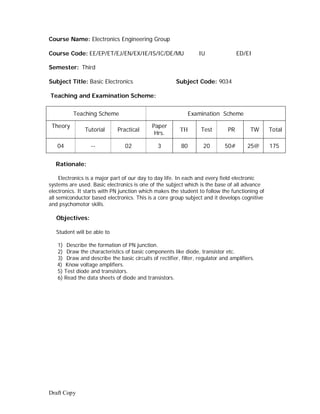
Teaching Scheme Examination Scheme
Theory Paper
Tutorial Practical TH
Th
TH Test PR TW Total
Hrs.
04 -- 02 3 80 20 50# 25@ 175
Rationale:
Electronics is a major part of our day to day life. In each and every field electronic
systems are used. Basic electronics is one of the subject which is the base of all advance
electronics. It starts with PN junction which makes the student to follow the functioning of
all semiconductor based electronics. This is a core group subject and it develops cognitive
and psychomotor skills.
Objectives:
Student will be able to
1) Describe the formation of PN junction.
2) Draw the characteristics of basic components like diode, transistor etc.
3) Draw and describe the basic circuits of rectifier, filter, regulator and amplifiers.
4) Know voltage amplifiers.
5) Test diode and transistors.
6) Read the data sheets of diode and transistors.
Draft Copy
2. Learning Structure
Use of principle and working of rectifier, filters, amplifiers using
Application semiconductor Diode and Transistors
Small
Dc signal
Power Transistor
supply amplifier
Procedures
Filter Biasing of
circuits transistors
Zener
Regulator
Rectifiers
HWR & FWR
PN junction BJT
Special Semiconductor JFET
Concept Diodes diode UJT
Active Devices
P-type and N-type
Facts Passive Devices Semiconductor
Physics
Draft Copy
3. Contents: Theory
Chapter Name of the Topic Hours Marks
1 Semiconductor diode 12 16
Rectifying diode
Review of P-type and N-type semiconductor
Junction of P-type & N-type i.e. PN junction
Barrier voltage , depletion region ,Junction Capacitance
Forward biased & reversed biased junction
Diode symbol , circuit diagram for characteristics
(forward
& reversed )
Characteristics of PN junction diode
Specifications:-
Forward voltage drop , Reversed saturation current,
maximum forward current , power dissipation
Package view of diodes of different power ratings (to
be shown during practical hours)
Zener diode
construction ( reference to doping level )
Symbol , circuit diagram for characteristics ( forward &
reversed )
Avalanche & zener breakdown
Specifications:-
Zener voltage , power dissipation , break over current,
dynamic resistance & maximum reverse current
Special diodes
Point contact diode , Schottky diode
Optical Diodes
LED, IRLED, photo diode, and laser diode.
Symbol, operating principle & applications of each.
2 Rectifiers & Filters 10 12
Need of rectifier , definition
Types of rectifier – Half wave rectifier, Full wave
rectifier,
(Bridge & centre tapped )
Circuit operation
Input/output waveforms for voltage & current
Average (dc) value of current & voltage ( no
derivation)
Ripple , ripple factor , ripple frequency , PIV of diode
used , transformer utilization factor , efficiency of
rectifier.
Comparison of three types of rectifier
Need of filters
Types of filters
A] shunt capacitor B] Series inductor C] LC filter
D] π filter
Draft Copy
4. Circuit operation, dc output voltage , ripple factor
( formula) , ripple frequency , Dependence of ripple
factor on load .
Input/output waveforms , limitations & advantages
3 Transistors 12 16
1] Bipolar junction transistor(BJT)
Introduction , Basic concept
Types of transistors , structure & symbols
Transistor operation
Conventional current flow , relation between different
currents in transistor
Transistor amplifying action
Transistor configurations:- CB , CE & CC
Circuit diagram to find the characteristics
Input/output characteristics
Transistor parameters- input resistance, output
resistance,
α , β & relation between them.
Comparison between three configurations
Transistor specifications:-
VCE Sat ,IC Max , VCEO , ICEO, α , β VCE Breakdown , Power
dissipation ( to be explained during practical using
data sheets)
Testing of transistor using multimeter( To be shown
during practical)
Construction, working principle, characteristics of
Photo transistor
Introduction to opto-coupler
2] Unipolar transistor (JFET)
Construction, working principle & characteristics.
3] Unijunction Transistor(UJT)
Construction, working principle& characteristics.
4 Biasing of BJT 10 12
Introduction , need of biasing , concept of dc load line
, selection of operating point (Q point) , need of
stabilization of Q point, ( thermal run away concept)
Types of biasing circuits
A] Fixed biased circuit
B] Base biased with emitter feed back
C] Base biased with collector feed back
D] Voltage divider
E] Emitter biased
Circuit operation of each circuit.
Introduction to two port n/w
Hybrid model for CE.
Draft Copy
5. 5 Regulated power supply 08 08
What is regulator?
Need of regulators , voltage regulation factor
Concept of load regulation & line regulation
Basic zener diode voltage regulator
Linear Regulators
Basic block diagram of dc power supply
Transistorised series & shunt regulator – circuit diagram
& operation.
Regulator IC’s – 78xx, 79xx, 723 as fixed, variable &
dual regulator.
6 Small signal amplifiers 12 16
Concept of amplification
Small signal amplifier using BJT
Graphical analysis
Determination of current , voltage & power gain ,
Input & output resistance , phase shift between input
& output.
AC Load Line
Function of input & output coupling capacitors &
criteria
for the value selection.
Function of emitter bypass capacitor & its value
selection.
AC equivalent circuit of transistor CE amplifier.
Single stage CE amplifier with voltage divider bias.
Its explanation.
Frequency response of single stage CE Amplifier, Bell,
Decibel unit. Bandwidth & its significance. Effect of
coupling & emitter bypass capacitor on bandwidth.
Introduction to CB & CC amplifier & List of
applications.
Cascade Amplifiers ( Multistage Amplifier)
Need of Multistage Amplifiers, Gain of amplifier.
Types of amplifier coupling – RC, transformer &
Direct coupling.
Two stage amplifier circuit diagram , working,
frequency
Response , merits & demerits & applications of each.
Total 64 80
Practical:
Skills to be developed:
Draft Copy
6. Intellectual Skills:
1. Identification and selection of components
2. Interpretation of circuits
3. Understand working of Regulated dc power supply
Motor skills:
1. Ability to draw the circuits
2. Ability to measure various parameters
3. Ability to test the components using multimeter
4. Follow standard test procedures
List of Practical:
1] Forward & Reverse characteristics of diode
2] Forward & Reverse characteristics of Zener diode
3] Study of Rectifiers a] Half wave b] Full wave
4] Study of filter circuits. a] Capacitor Filter b] Inductor filter.
5] Input & output characteristics of transistor in CE mode
6] Input & output characteristics of transistor in CB mode
7] Characteristics of FET
9] Characteristics of UJT
10] Zener Diode Regulator
11] Transistor series and shunt regulator
11] Single stage common emitter amplifier
12] Two stage RC coupled amplifier [Frequency response]
Learning Resources:
1. Books:
Sr. Author Title Publisher
No.
01 N.N.Bhargava, D.C. Basic Electronics & Tata McGraw Hill
Kulashreshtha, S.C. Linear Circuits
Gupta - TTTI
Chandigharh
02 Alberrt Malvino Electronic Principles Tata McGraw Hill
David J.Bates
03 Allen. Mottershead Electronic Devices & Prentice Hall of India
Components’
04 NIIT Basic Electronics Prentice Hall of India
&Devices
05 Grob Bernard Basic Electronics Tata McGraw Hill
06 David J. Bell Electronics Devices & Prentice Hall of India
Circuits
Draft Copy