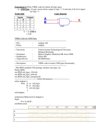
1. Experiment 1: Write VHDL code for realize all logic gates.
a) AND Gate: A Logic circuit whose output is logic ‘1’ if and only if all of its inputs
are logic ‘1’.
Truth table Logic diagram
Inputs Output
A 2
A B Y
1 Y
0 0 0 B 3
0 1 0
1 0 0 AND2
1 1 1
Y = A AND B
= A.B
VHDL Code for AND Gate:
-------------------------------------------------------------------------------
-- File : andgate.vhd
-- Entity : andgate
-------------------------------------------------------------------------------
-- University : Vishweswaraia Technological University
Belgaum,Karnataka
-- Simulators : Mentor Graphics Modelsim OR Active HDL
-- Synthesizers : Xilinx ISE
-- Target Device : XC4000 Series
-------------------------------------------------------------------------------
-- Description : VHDL code to realize AND gate functionality
-------------------------------------------------------------------------------
--The IEEE standard 1164 package, declares std_logic, etc.
library IEEE;
use IEEE.std_logic_1164.all;
use IEEE.std_logic_arith.all;
use IEEE.std_logic_unsigned.all;
---------------------------------- Entity Declarations -------------------------
entity andgate is
Port( A : in std_logic;
B : in std_logic;
Y : out std_logic
);
end andgate;
architecture Behavioral of andgate is
begin
Y<= A and B ;
end Behavioral;
500 1000 1
500 2000 2500 3000 ns
a
b
y
2. b)OR Gate: A logic gate whose output is logic ‘0’ if and only if all of its inputs are
logic ‘0’.
Truth table Logic diagram
Inputs Output
A 2
A B Y 1 Y
0 0 0 B 3
0 1 1
1 0 1 OR2
1 1 1
Y = A OR B
=A+B
VHDL Code for OR Gate:
-------------------------------------------------------------------------------
-- File : orgate.vhd
-- Entity : orgate
-------------------------------------------------------------------------------
-- University : Vishweswaraia Technological University
Belgaum,Karnataka
-- Simulators : Mentor Graphics Modelsim OR Active HDL
-- Synthesizers : Xilinx ISE
-- Target Device : XC4000 Series
-------------------------------------------------------------------------------
-- Description : VHDL code to realize OR gate functionality
-------------------------------------------------------------------------------
--The IEEE standard 1164 package, declares std_logic, etc.
library IEEE;
use IEEE.std_logic_1164.all;
use IEEE.std_logic_arith.all;
use IEEE.std_logic_unsigned.all;
---------------------------------- Entity Declarations -------------------------
entity orgate is
Port( A : in std_logic;
B : in std_logic;
Y : out std_logic
);
end orgate;
architecture Behavioral of orgate is
begin
Y<= A or B ;
end Behavioral; 500 1000 1500 2000 2500 3000 3500 4000 4500
a
b
y
3. c) NOT Gate: A logic gate whose input is complement of its input.
Truth table Logic diagram
Input Output
A Y A Y
0 1
1 0 INV
Y = NOT A
VHDL Code for NOT Gate:
-------------------------------------------------------------------------------
-- File : notgate.vhd
-- Entity : notgate
-------------------------------------------------------------------------------
-- University : Vishweswaraia Technological University
Belgaum,Karnataka
-- Simulators : Mentor Graphics Modelsim OR Active HDL
-- Synthesizers : Xilinx ISE
-- Target Device : XC4000 Series
-------------------------------------------------------------------------------
-- Description : VHDL code to realize NOT gate functionality
-------------------------------------------------------------------------------
--The IEEE standard 1164 package, declares std_logic, etc.
library IEEE;
use IEEE.std_logic_1164.all;
use IEEE.std_logic_arith.all;
use IEEE.std_logic_unsigned.all;
---------------------------------- Entity Declarations -------------------------
entity notgate is
Port( A : in std_logic;
Y : out std_logic
);
end notgate;
architecture Behavioral of notgate is
begin
Y<= not A ;
end Behavioral;
500 1
000 1
500 2000 2500 3000 3500 4000 4500 ns
a
y
4. d) NAND Gate: A logic gate which gives logic ‘0’ output if and only if all of its
inputs are logic ‘1’
Truth table Logic diagram
Inputs Output
A B Y A 2
1 Y
0 0 0 B 3
0 1 1
1 0 1 NAND2
1 1 1
Y= A NAND B
=(A. B)
VHDL Code for NAND Gate:
-------------------------------------------------------------------------------
-- File : nandgate.vhd
-- Entity : nandgate
-------------------------------------------------------------------------------
-- University : Vishweswaraia Technological University
Belgaum,Karnataka
-- Simulators : Mentor Graphics Modelsim OR Active HDL
-- Synthesizers : Xilinx ISE
-- Target Device : XC4000 Series
-------------------------------------------------------------------------------
-- Description : VHDL code to realize NAND gate functionality
-------------------------------------------------------------------------------
--The IEEE standard 1164 package, declares std_logic, etc.
library IEEE;
use IEEE.std_logic_1164.all;
use IEEE.std_logic_arith.all;
use IEEE.std_logic_unsigned.all;
---------------------------------- Entity Declarations -------------------------
entity nandgate is
Port( A : in std_logic;
B : in std_logic;
Y : out std_logic
);
end nandgate;
architecture Behavioral of nandgate is
begin
Y<= A nand B ;
end Behavioral;
500 1
000 1
500 2000 2500 3000 3500 4000 4500 ns
a
b
y
5. e) NOR Gate: A logic gate whose output logic ‘1’ if and only if all of its inputs are
logic ‘0’
Truth table Logic diagram
Inputs Output
A B Y A 2
0 0 0 1 Y
0 1 1 B 3
1 0 1 NOR2
1 1 1
Y= A NOR B
=(A+ B)
VHDL Code for NOR Gate:
-------------------------------------------------------------------------------
-- File : norgate.vhd
-- Entity : norgate
-------------------------------------------------------------------------------
-- University : Vishweswaraia Technological University
Belgaum,Karnataka
-- Simulators : Mentor Graphics Modelsim OR Active HDL
-- Synthesizers : Xilinx ISE
-- Target Device : XC4000 Series
-------------------------------------------------------------------------------
-- Description : VHDL code to realize NOR gate functionality
-------------------------------------------------------------------------------
--The IEEE standard 1164 package, declares std_logic, etc.
library IEEE;
use IEEE.std_logic_1164.all;
use IEEE.std_logic_arith.all;
use IEEE.std_logic_unsigned.all;
---------------------------------- Entity Declarations -------------------------
entity norgate is
Port( A : in std_logic;
B : in std_logic;
Y : out std_logic
);
end norgate;
architecture Behavioral of norgate is
begin
Y<= A nor B ;
end Behavioral;
2000 2500 3000 3500 4000 ns
a
b
y
6. f) EX-OR (Exclusive OR): A logic gate whose output is logic ‘0’ when all the inputs
are equal and logic ‘1’ when they are un equal.
Truth table Logic diagram
Inputs Output
A B Y A 2
0 0 0 1 Y
0 1 1 B 3
1 0 1 XOR2
1 1 0
Y= A EX-OR B
= A (+)B
= A.B + A.B
VHDL Code for EX-OR Gate:
-------------------------------------------------------------------------------
-- File : xorgate.vhd
-- Entity : xorgate
-------------------------------------------------------------------------------
-- University : Vishweswaraia Technological University
Belgaum,Karnataka
-- Simulators : Mentor Graphics Modelsim OR Active HDL
-- Synthesizers : Xilinx ISE
-- Target Device : XC4000 Series
-------------------------------------------------------------------------------
-- Description : VHDL code to realize EX-OR gate functionality
-------------------------------------------------------------------------------
--The IEEE standard 1164 package, declares std_logic, etc.
library IEEE;
use IEEE.std_logic_1164.all;
use IEEE.std_logic_arith.all;
use IEEE.std_logic_unsigned.all;
---------------------------------- Entity Declarations -------------------------
entity xorgate is
Port( A : in std_logic;
B : in std_logic;
Y : out std_logic
);
end xorgate;
architecture Behavioral of xorgate is
begin
Y<= A xor B ;
end Behavioral; ns
200 400 600 800 1000 1200 1400 1600 1800 2000 2200
a
b
y
7. g) EX-NOR (Exclusive -NOR) gate: A logic gate that prodices a logic ‘1’ only when
the two inputs are equal
Truth table Logic diagram
Inputs Output
A B Y A 2
0 0 0 1 Y
0 1 1 B 3
1 0 1
XNOR2
1 1 0
Y= A XNOR B
= (A (+)B)
= (A.B) + A.B
VHDL Code for EX-NOR Gate:
-------------------------------------------------------------------------------
-- File : xnorgate.vhd
-- Entity : xnorgate
-------------------------------------------------------------------------------
-- University : Vishweswaraia Technological University
Belgaum,Karnataka
-- Simulators : Mentor Graphics Modelsim OR Active HDL
-- Synthesizers : Xilinx ISE
-- Target Device : XC4000 Series
-------------------------------------------------------------------------------
-- Description : VHDL code to realize EX-NOR gate functionality
-------------------------------------------------------------------------------
--The IEEE standard 1164 package, declares std_logic, etc.
library IEEE;
use IEEE.std_logic_1164.all;
use IEEE.std_logic_arith.all;
use IEEE.std_logic_unsigned.all;
---------------------------------- Entity Declarations -------------------------
entity xnorgate is
Port( A : in std_logic;
B : in std_logic;
Y : out std_logic
);
end xnorgate;
architecture Behavioral of xnorgate is
begin
Y<= A xnor B ;
end Behavioral; ns
200 400 600 800 1
000 1
200 1
400 1
600 1
800 2000 2200
a
b
y
8. Experiment 2: Write a VHDL program for the following combinational designs.
a) 2 to 4 decoder: A decoder is a digital logic circuit that converts n-bits binary input
code in to M output lines. OR It is a logic circuit that decodes from binary to octal,
decimal, Hexa-decimal or any other code such as 7-segment etc.
EN SEL(1) SEL(0)
INST1 INST2
INV INV
U5
2
3
4
1 D0
NAND3
U6
2
3
4
1 D1
NAND3
Block Diagram of Decoder U7
2
3
4
1 D2
NAND3
U8
2
3
4
1 D3
NAND3
Logic Diagram of 2:4 Decoder
EN Inputs Output
Sel(1) Sel(0) D
1 X X 0
0 0 0 D0
0 0 1 D1
0 1 0 D2
0 1 1 D3
Truth table
9. -------------------------------------------------------------------------------
-- File : decoder24.vhd
-- Entity : decoder24
-------------------------------------------------------------------------------
-- University : Vishweswaraia Technological University
Belgaum,Karnataka
-- Simulators : Mentor Graphics Modelsim Or Active HDL
-- Synthesizers : Xilinx ISE
-- Target Device : XC4000 Series
-------------------------------------------------------------------------------
-- Description : 2 to 4 DECODER
-------------------------------------------------------------------------------
--The IEEE standard 1164 package, declares std_logic, etc.
library IEEE;
use IEEE.std_logic_1164.all;
use IEEE.std_logic_arith.all;
use IEEE.std_logic_unsigned.all;
---------------------------------- Entity Declarations -------------------------
entity decoder24 is
generic(
N: INTEGER :=2;
M: INTEGER :=4 );
port (
EN : in STD_LOGIC;
SEL: in STD_LOGIC_VECTOR (N-1 downto 0);
D: out STD_LOGIC_VECTOR (M-1 downto 0) );
end decoder24;
architecture decoder24_arch of decoder24 is
signal aux: INTEGER;
begin
aux<=conv_integer(SEL);
process(EN,aux)
begin
if (EN=' ) then
1'
for i in 0 to M-1 loop
if aux=i then
D(i)<=' ;
1'
else
D(i)<=' ;
0'
end if;
end loop;
else
for i in 0 to M-1 loop
D(i)<=' ;
0'
end loop;
end if;
end process;
end decoder24_arch;
10. Simulator Waveforms for 2:4 Decoder:
500 10 0 0 15 0 0 2000 2500 ns
EN
SEL 0 1 2 3 0 1 2 3 0 1 2
D 0000 0 0 10 0 10 0 10 0 0 0001 0 0 10 0 10 0 10 0 0 0001 0 0 10 0 10 0
D (3 )
D (2 )
D (1 )
D (0 )
11. b) 8 to 3 (Encoder without & with priority)
Encoder: A logic circuit that produces coded binary outputs from uncoded inputs.
Priority encoder: Whenever two or more inputs are applied at a time, internal
hardware will check this condition and if the priority is set such that higher numbered
input should be taken into account and remaining are considered as don’t care then
output code will be appear will be “higher numbered input”.
Truth table for 8-input priority encoder
EN DIN (7:0) EOUT
0 XXXXXXXX 0
1 XXXXXXX0 0
1 XXXXXX 01 1
1 XXXXX 011 2
1 XXXX 0 111 3
1 XXX 0 1 111 4
1 XX 0 1 1 111 5
1 X0 1 1 1 111 6
1 0 1 1 1 1 111 7
1 1 1 1 1 1 111 0
Block Diagram of priority encoder
12. -------------------------------------------------------------------------------
-- File : pencoder.vhd
-- Entity : pencoder
-------------------------------------------------------------------------------
-- University : Vishweswaraia Technological University
Belgaum,Karnataka
-- Simulators : Mentor Graphics Modelsim Or Active HDL
-- Synthesizers : Xilinx ISE
-- Target Device : XC4000 Series
-------------------------------------------------------------------------------
-- Description : 8-input priority encoder
-------------------------------------------------------------------------------
--The IEEE standard 1164 package, declares std_logic, etc.
library IEEE;
use IEEE.std_logic_1164.all;
use IEEE.std_logic_arith.all;
use IEEE.std_logic_unsigned.all;
---------------------------------- Entity Declarations -------------------------
entity pencoder is
port (
X: in STD_LOGIC_VECTOR (7 downto 0);
E: in STD_LOGIC;
Y: out STD_LOGIC_VECTOR (2 downto 0);
A: out STD_LOGIC
);
end pencoder;
architecture pencoder_arch of pencoder is
begin
pe: process(x,E)
variable k: integer;
begin
y <= "000";
A <= ' ;0'
if E = ' then
1'
for j in 0 to 7 loop
if x(j) = ' then
1'
y <= conv_std_logic_vector(j,3);
A <= ' ;
1'
end if;
end loop;
end if;
end process pe;
end pencoder_arch;
13. Simulator Waveforms for 8-input priority encoder:
300 400 500 600 700 800 900 1000 1 00
1 ns
E
x 05 0A 0F 14 19 1E 23 28 2D 32
x(7)
x(6)
x(5)
x(4)
x(3)
x(2)
x(1)
x(0)
y 2 3 4 5
y(2)
y(1)
y(0)
A
14. c) 8 :1 Multiplexer: The multiplexer is a combinational circuit which accepts several data
inputs and allows only one of them AT A TIME to get through to the output.
EN SEL(2) SEL(1) SEL(0)
ENABLE INV1
INV3 INV2
2 U1
3
4 1
D0
5
D0 6
AND5
D1 0 EN
2 U2
3
4 1
1
5
D1 6
D2 2 2
3
AND5
U3
D3 3 D2
4
5
6
1
O/PData Output
AND5
Data D4 4 2 U4
8:1
3 2 U9
Inputs 5 Y 4 1 3
D5
5 4
D3 6 5
Y
6 AND5 1
6
D6
2 U5 7
7
3 8
4 1 9
5
D4 6
OR8
D7 2
3
AND5
U6
4 1
5
D5 6
AND5
2 U7
3
SEL0
4 1
5
D6 6
AND5
SEL1 2
3
4
5
U8
1
D7
SEL2
6
AND5
Control Inputs
Block Diagram of 8:1 Mux Logic Diagram
EN CONTROL INPUTS OUTPUT(Y)
SEL(3) SEL(3) SEL(3) (Selected
Inputs)
0 0 0 0 D0
1 0 0 1 D1
1 0 1 0 D2
1 0 1 1 D3
1 1 0 0 D4
1 1 0 1 D5
1 1 1 0 D6
1 1 1 1 D7
15. -------------------------------------------------------------------------------
-- File : mux8_1.vhd
-- Entity : mux8_1
-------------------------------------------------------------------------------
-- University : Vishweswaraia Technological University
Belgaum,Karnataka
-- Simulators : Mentor Graphics Modelsim
-- Synthesizers : Xilinx ISE
-- Target Device : XC4000 Series
-------------------------------------------------------------------------------
-- Description : 8 TO 1 MULTIPLEXOR
-------------------------------------------------------------------------------
--The IEEE standard 1164 package, declares std_logic, etc.
library IEEE;
use IEEE.std_logic_1164.all;
use IEEE.std_logic_arith.all;
use IEEE.std_logic_unsigned.all;
---------------------------------- Entity Declarations -------------------------
entity mux8_1 is
port (
D: in STD_LOGIC_VECTOR (7 downto 0);
EN: in STD_LOGIC;
SEL: in STD_LOGIC_VECTOR (2 downto 0);
Y: out STD_LOGIC );
end mux8_1;
architecture mux8_1_arch of mux8_1 is
begin
process(EN,SEL,D)
begin
if(EN=' )then
1'
y<=' ;
0'
else
case SEL is
when "000" => y <= D(0);
when "001" => y <= D(1);
when "010" => y <= D(2);
when "011" => y <= D(3);
when "100" => y <= D(4);
when "101" => y <= D(5);
when "110" => y <= D(6);
when others=> y <= D(7);
end case;
end if;
end process;
end mux8_1_arch;
16. Simulator Waveforms for 8:1 Multiplexer:
1000 2000 3000 4000 5000 6000 7000 8000 9000 ns
D
D(7)
D(6)
D(5)
D(4)
D(3)
D(2)
D(1)
D(0)
EN
SEL 0 1 2 3 4 5 6 7
Y
17. d) 4-bit Binary to Gray converter.
Binary –It is a number system, which has only two states ‘0’ (high) and ‘1’ (low)
Gray- In Gray code “ Every new code differs from the previous interms of single
bit” only one bit changes between successive numbers.
Decimal
Binary Gray B3 G3
0 0000 0000 U3
1 0001 0001
2 0010 0011 B2
2
3
1 G2
3 0011 0010
4 0100 0110 XOR2
5 0101 0111 U2
6
7
0110
0111
0101
0100 B1
2
3
1 G1
8 1000 1100
XOR2
9 1001 1101
10 1010 1111 U1
11 1011 1110
B0
2
1 G0
12 1100 1010 3
13 1101 1011 XOR2
14 1110 1001
15 1111 1000
18. ------------------------------------------------------------------------------
-- File :b2g.vhd
-- Entity :b2g
-------------------------------------------------------------------------------
-- University :Vishweswaraia Technological University
Belgaum,Karnataka
-- Simulators :Mentor Graphics Modelsim
-- Synthesizers :Xilinx ISE
-- Target Device :XC4000 Series
-------------------------------------------------------------------------------
-- Description : 4-BIT BINARY TO GRAY CONVERTOR
-------------------------------------------------------------------------------
--The IEEE standard 1164 package, declares std_logic, etc.
library IEEE;
use IEEE.std_logic_1164.all;
use IEEE.std_logic_arith.all;
use IEEE.std_logic_unsigned.all;
---------------------------------- Entity Declarations -------------------------
entity b2g is
port (
B3,B2,B1,B0: in STD_LOGIC;
G3,G2,G1,G0: out STD_LOGIC
);
end b2g;
architecture b2g_arch of b2g is
begin
G3<=B3;
G2<=B2 xor B3;
G1<=B1 xor B2;
G0<=B0 xor B1;
end b2g_arch;
Simulator Waveforms for 4-Bit Binary to Gray Conversion:
200 400 600 800 1000 1200 1400 1600 1800 ns
B 0000 0001 001 001 01
0 1 00 0101 010
1 01 1
1 1000 1001 1 0
01 1 1
01 100
1 101
1 11
10 11
11
G 0000 0001 001 001 010
1 0 1 01 1
1 0101 0100 100
1 101
1 11
11 11
10 1 0
01 1 1
01 1001 1000
19. e) Multiplexer, Demultiplexer, comparator.
Multiplexer: Ref Exp 2(b)
Demultiplexer: Demultiplexer is a combinational circuit that accepts single input and
distributes it several outputs (Selectively distributes it to 1 of N output channels) &
Exhastly reverse of the multiplexer.
EN SEL(2) SEL(1) SEL(0)
ENABLE INV3 INV2 INV1
0 D0 2
3
4
U1
1 D0
EN 1 D1 Y 5
6
AND5
2 D2
2 U2
D1
3
4 1
5
D3
6
Data Input O/P 1:8
3 2
AND5
U3
D2
3
Demux 4 D4 4
5
1
Y
6
AND5
5 D5 2
3
4
U4
1 D3
D6
5
6 6
AND5
D7
2 U5
7 D4
3
4 1
5
6
AND5
2 U6
3
4 1 D5
Data Outputs 5
SEL0
6
AND5
2 U7
3
D6
SEL1 4
5
6
AND5
1
SEL2 2
3
4
U8
1 D7
5
Control Input 6
AND5
Block Diagram of 1:8 Demux Logic Diagram
Truth Table
EN CONTROL INPUTS OUTPUTS
SEL(3) SEL(3) SEL(3)
0 X X X 0
1 0 0 0 D0=Y
1 0 0 1 D1=Y
1 0 1 0 D2=Y
1 0 1 1 D3=Y
1 1 0 0 D4=Y
1 1 0 1 D5=Y
1 1 1 0 D6=Y
1 1 1 1 D7=Y
20. -------------------------------------------------------------------------------
-- File : demux.vhd
-- Entity : demux
-------------------------------------------------------------------------------
-- University : Vishweswaraia Technological University
Belgaum,Karnataka
-- Simulators : Mentor Graphics Modelsim
-- Synthesizers : Xilinx ISE
-- Target Device : XC4000 Series
-------------------------------------------------------------------------------
-- Description : 1:8 DEMULTIPLEXOR
-------------------------------------------------------------------------------
--The IEEE standard 1164 package, declares std_logic, etc.
library IEEE;
use IEEE.std_logic_1164.all;
use IEEE.std_logic_arith.all;
use IEEE.std_logic_unsigned.all;
---------------------------------- Entity Declarations -------------------------
entity demux8_1 is
port ( Y : in STD_LOGIC;
EN : in STD_LOGIC;
SEL : in STD_LOGIC_VECTOR (2 downto 0);
D : out STD_LOGIC_VECTOR (7 downto 0) );
end demux8_1;
architecture demux8_1_arch of demux8_1 is
begin
process(EN,SEL,Y)
begin
if(EN=' )then
1'
D<=(others=>' );
0'
else
case SEL is
when "000" => D(0)<=Y;
when "001" => D(1)<=Y;
when "010" => D(2)<=Y;
when "011" => D(3)<=Y;
when "100" => D(4)<=Y;
when "101" => D(5)<=Y;
when "110" => D(6)<=Y;
when others=> D(7)<=Y;
end case;
end if;
end process;
end demux8_1_arch;
21. Simulator Waveforms for 1: Demultiplexer:
500 1
000 1
500 2000 2500 3000 3500 ns
Y
EN
SEL 0 1 2 3 4 5 6 7
D 00 02 0A 2A AA
D(7)
D(6)
D(5)
D(4)
D(3)
D(2)
D(1)
D(0)
22. Comparator: A circuit that compares two numbers and produces an output
indicating whether they are equal. It may also indicate which number is greater if they
are unequal. Ex: ‘1’ bit comparator
Truth table:
Comparing Outputs
inputs
A B Y=(A>B) Y=(A<B) Y=(A=B)
0 0 0 0 1
0 1 0 1 0
1 0 1 0 0
1 1 0 0 1
:
A 2
U1
1
AB
Y(A<B)
3
INV1
AND2
U3
2
3
1 Y(A=B)
NOR2
U2
B
2
3
1 Y(A>B)
AND2 AB
INV2
23. -------------------------------------------------------------------------------
-- File : bitcomp.vhd
-- Entity : bitcomp
-------------------------------------------------------------------------------
-- University : Vishweswaraia Technological University
Belgaum,Karnataka
-- Simulators : Mentor Graphics Modelsim
-- Synthesizers : Xilinx ISE
-- Target Device : XC4000 Series
-------------------------------------------------------------------------------
-- Description : SINGLE BIT MAGNITUDE COMPARATOR.
-------------------------------------------------------------------------------
--The IEEE standard 1164 package, declares std_logic, etc.
library IEEE;
use IEEE.std_logic_1164.all;
use IEEE.std_logic_arith.all;
use IEEE.std_logic_unsigned.all;
---------------------------------- Entity Declarations -------------------------
entity bitcomp is
port (
A: in STD_LOGIC;
B: in STD_LOGIC;
sel: in STD_LOGIC_VECTOR(1 DOWNTO 0);
Y: out BOOLEAN
);
end bitcomp;
architecture bitcomp_arch of bitcomp is
begin
process(A,B,sel)
begin
case sel is
when "00" => y <= A=B;
when "01" => y <= A>B;
when "10" => y <= A<B;
when others => y <= FALSE ;
end case;
end process;
end bitcomp_arch;
24. Simulator Waveforms for SINGLE BIT MAGNITUDE
COMPARATOR:
500 1
000 1
500 2000 2500 3000 3500 ns
A
B
sel 0 1 2 3 0
Y true false true false true false true false true
25. Experiment 3: Write a VHDL code to describe the functions of full adder using
different modeling styles.
A logic circuit for the addition of two one bit numbers is called half adder (sum
and carry are output) and a logic circuit that accepts two one-bit signal and
Carry-in as inputs and produces their sum and carry as outputs is called full adder.
Truth table for Full adder Truth table for Half adder
INPUTS OUTPUTS INPUTS OUTPUTS
A B Cin SUM CARRY
0 0 0 0 0 A B SUM CARRY
0 0 1 1 0 0 0 0 0
0 1 0 1 0 0 1 1 0
0 1 1 0 1
1 0 0 1 0 1 0 1 0
1 0 1 0 1 1 1 0 1
1 1 0 0 1
1 1 1 1 1
U1 U10
A A
B
2
3 1 A(+)B(+)CSUM 2
1 SUM
Cin B
4 3
A(+)B
XOR3 XOR2
U2
2 U11
1 2
3 1 CARRY
3
AND2
U3 U5 AND2 A.B
2 2
1 3 1 CARRY
3 4
AND2 OR3
U4
2
1 A.B + B.Cin + A.Cin
3
AND2
Full adder using 2-Half adder
26. VHDL Code for HALF ADDER
-- File : HA.vhd
-- Entity : HA
-- Architecture : HA_arch
-------------------------------------------------------------------------------
-- University : Vishweswaraia Technological University
Belgaum,Karnataka
-- Simulators : Mentor Graphics Modelsim
-- Synthesizers : Xilinx ISE
-- Target Device : XC4000 Series
-------------------------------------------------------------------------------
-- Description : HALF ADDER.
-------------------------------------------------------------------------------
--The IEEE standard 1164 package, declares std_logic, etc.
library IEEE;
use IEEE.std_logic_1164.all;
use IEEE.std_logic_arith.all;
use IEEE.std_logic_unsigned.all;
---------------------------------- Entity Declarations -------------------------
entity HA is
port(
A,B : in STD_LOGIC;
S,CY : out STD_LOGIC
);
end HA;
architecture HA_arch of HA is
begin
S<= A XOR B;
CY<= A AND B;
end HA_arch;
27. VHDL Code for FULL ADDER
-- STRUCTURAL MODELING-A set of interconnect with different COMPONENT
-- File : FA.vhd
-- Entity : FA
-- Architecture : FA_arch
-------------------------------------------------------------------------------
-- University : Vishweswaraia Technological University
Belgaum,Karnataka
-- Simulators : Mentor Graphics Modelsim
-- Synthesizers : Xilinx ISE
-- Target Device : XC4000 Series
-------------------------------------------------------------------------------
-- Description : FULL ADDER.
-------------------------------------------------------------------------------
--The IEEE standard 1164 package, declares std_logic, etc.
library IEEE;
use IEEE.std_logic_1164.all;
use IEEE.std_logic_arith.all;
use IEEE.std_logic_unsigned.all;
---------------------------------- Entity Declarations -------------------------
entity FA is
port(
A,B,Cin : in STD_LOGIC;
SUM,CARRY : out STD_LOGIC
);
end FA;
architecture STRUCTURAL of FA is
signal sum1,cy1,cy2:std_logic;
component HA
port(
A,B : in STD_LOGIC;
S,CY : out STD_LOGIC
);
end component ;
begin
u1: HA port map(A=>A, B=>B, S=>SUM1, CY=>CY1);
u2: HA port map(A=>SUM1, B=>Cin, S=>SUM, CY=>CY2);
CARRY<= cy1 OR cy2;
end STRUCTURAL;
28. -- DATAFLOW MODELING-A set of concurrent assignment statements.
architecture DATAFLOW of FA is
begin
SUM<= A XOR B XOR Cin;
CARRY<= (A AND B) OR (Cin AND A)OR (Cin AND B);
end DATAFLOW;
-- BEHAVIORAL MODELING-A set of sequential assignment statements according to
-- the behavior of the design. (Process is single concurrent statement, which has
sequential statements.)
architecture BEHAVIOR of FA is
begin
process(A,B,Cin)
begin
SUM<= A XOR B XOR Cin;
CARRY<= (A AND B) OR (Cin AND A)OR (Cin AND B);
end process;
end BEHAVIOR;
29. Simulator waveforms of HALF ADDER
1 2 3 4 5 6 7 8 9 us
A
B
SUM
CARRY
Simulator waveforms of FULL ADDER
100 200 300 400 500 600 700 800 900 ns
A
B
Cin
SUM
CARRY
30. Experiment 4: Write a model for 32 bit ALU using the schematic diagram
Shown below example
ALU should use the combinational logic to calculate an output based on the four
bit Opcode input.
ALU should pass the result to the out bit when enable line is high and tri-state
when low enable.
ALU should decode the 4-bit op-code according to the given in example below
Opcode ALU operation
1 A+B
2 A–B
3 A Complement
4 A*B
5 A AND B
6 A OR B
7 A NAND B
8 A XOR B
Function table for ALU
Enable Mode Opcode Functional description
0 X XXXX Y<=”Z” (Tri-stated)
1 0 0001 Y<= A + B ;
1 0 0010 Y<= A – B;
1 0 0011 Y <= A(15:0)* B(15:0)* ;
1 1 0100 Y <= NOT A (Complement)
1 1 0101 Y <= A AND B (AND Operation)
1 1 0110 Y <= A OR B (OR Operation)
1 1 0111 Y <= A NAND B (NAND Operation)
1 1 1000 Y <= A XOR B (XOR Operation)
1 X 1001 Y <= Y (ALU is ideal or previous data is
latched for all other higher opcodes.
1 X 10¹⁰ “ “
1 X 10¹¹ “ “
1 X 1100 “ “
1 X 1101 “ “
1 X 1110 “ “
1 X 1111 “ “
31. ARTHAMETIC LOGIC UNIT (ALU)
ALU is logic circuit which is able to perform different arithmetic and logical
function basically ALU is the heart of central processing unit (CPU).
Cin Cin + 1 (CY)
Data One stage of
i/p 32 Arithmetic
A 32 circuit
B
4 0 32
Opcode [3:0] 0
2:1
Enabl 32 Mux
32 Y
Control
e 1
Signals 1 (Data o/p)
One stage of
Logic circuit
Mode
Mode : ‘0’____ Arthmatic operation
‘1’____Logic operation
Enable ‘0’ Y <= “ Z “
‘1’ Out put performed
Note: For A*B, A&B lower 16 bit [15:0] can be taken in to consideration.
32. VHDL Code for 8_bit ALU:
-- File : alu.vhd
-- Entity : alu
-------------------------------------------------------------------------------
-- University : Vishweswaraia Technological University
Belgaum,Karnataka
-- Simulators : Mentor Graphics Modelsim
-- Synthesizers : Xilinx ISE
-- Target Device : XC4000 Series
-------------------------------------------------------------------------------
-- Description : 8-bit ALU.
-------------------------------------------------------------------------------
--The IEEE standard 1164 package, declares std_logic, etc.
library IEEE;
use IEEE.Std_Logic_1164.all;
use IEEE.NUMERIC_STD.all;
---------------------------------- Entity Declarations -------------------------
-- NOTE : JUST BY CHANGING THE WIDTH OF INPUT AND OUTPUT
OF (31 DOWNTO O)
-- WILL BECOME 32-BIT ALU
--------------------------------------------------------------------------------
entity Alu is
port( Clk : in Std_Logic;
MODE,EN: in Std_Logic;
A,B : in Std_Logic_Vector(7 downto 0);
OPCODE : in Std_Logic_Vector(3 downto 0);
Y : out Std_Logic_Vector(7 downto 0));
end Alu;
architecture Alu_a of Alu is
signal C_s : Unsigned(7 downto 0);
begin
process (A, B,OPCODE,mode)
variable A_v : Unsigned(7 downto 0);
variable B_v : Unsigned(7 downto 0);
begin
A_v := Unsigned(A);
B_v := Unsigned(B);
if(EN=' )then
0'
C_s<=(others=>' );
Z'
if(mode=' )then
0'
case OPCODE is
when "0000" => C_s <= A_v + B_v;
when "0001" => C_s <= A_v - B_v;
when "0010" => C_s <= A_v(3 downto 0) * B_v(3 downto 0);
when others => C_s <= (others => ' );
0'
end case;
else
case opcode is
when "0011" => C_s <= not A_v;
33. when "0100" => C_s <= not B_v;
when "0101" => C_s <= A_v and B_v;
when "0110" => C_s <= A_v nand B_v;
when "0111" => C_s <= A_v or B_v;
when "1000" => C_s <= A_v nor B_v;
when "1001" => C_s <= A_v xor B_v;
when "1010" => C_s <= A_v xnor B_v;
when others => C_s <= (others => ' );
0'
end case;
end if;
end if;
end process;
process
begin
wait until Clk'
event and Clk = ' ;
1'
y <= Std_Logic_Vector(C_s);
end process ;
end Alu_a;
Simulator waveforms for 8_bit ALU:
50 100 150 200 250 300 350 ns
Clk
MODE
EN
A 08
B 04
OPCODE 0 1 2 3 4 3 4 5 6 7 8 9 A B C D
Y UU 04 20 00 F7 FB 00 FF 0C F3 0C F3 00
34. Experiment 5: Develop the VHDL code for the following flip-flops SR, D, JK & T.
Flip-flop: Flip-flop is a sequential logic circuit, which is ‘One ‘-bit memory
element. OR It is a basic memory element in digital systems (same as the bi-stable
multivibrator) It has two stable state logic ‘1’ and logic ‘0’.
Set Set
? Q ? Q
Clk o Clk
? Q ? Q
Rst Rst
o o
Positive
Edge-Triggered
-
Negative Edge Triggered
(a) S-R Flip-flop (Set-Reset)
In a memory device set and Reset is often required for synchronization of the
device in such case S-R Flip-flop is need & this is refereed as clocked set-reset.
Set-Reset Truth table
S R Q+ Action
0 0 Q No
Change
0 1 0 Reset
1 0 1 Set
1 1 - Illegal
35. VHDL Code for SR Flip-Flop:
-------------------------------------------------------------------------------
-- File : SRFF.vhd
-- Entity : SRFF
-------------------------------------------------------------------------------
-- University : Vishweswaraia Technological University
Belgaum,Karnataka
-- Simulators : Mentor Graphics Modelsim Or Active HDL
-- Synthesizers : Xilinx ISE
-- Target Device : XC4000 Series
-------------------------------------------------------------------------------
-- Description : SR Flip-Flop
-------------------------------------------------------------------------------
--The IEEE standard 1164 package, declares std_logic, etc.
library IEEE;
use IEEE.std_logic_1164.all;
use IEEE.std_logic_arith.all;
use IEEE.std_logic_unsigned.all;
---------------------------------- Entity Declarations -------------------------
entity SRFF is
port (
CLK, RST, S, R : in std_logic;
Q, Qn : out std_logic);
end SRFF;
architecture RTL of SRFF is
signal FF : std_logic;
begin
process (CLK, RST)
variable SR : std_logic_vector(1 downto 0);
begin
if (RST = ' ) then
0'
FF <= ' ;0'
elsif (CLK' event and CLK = ' ) then
1'
SR := S & R;
case SR is
when "01" => FF <= ' ; 0'
when "10" => FF <= ' ; 1'
when "11" => FF <= ' ; Z'
when others => FF <= FF;
end case;
end if;
end process;
Q <= FF ;
Qn <= not FF ;
end RTL;
36. Simulator waveforms for SR Flip-Flop:
200 400 600 800 1000 1200 1400 ns
CLK
RST
S
R
Q
Qn
(b) D- FF (Delay Flip-flop)
In D-Flip-flop the transfer of data from the input to the Output is delayed and
hence the name delay D-Flip-flop. The D-Type Flip-flop is either used as a
delay device or as a latch to store ‘1’ bit of binary information.
D input transferred to Q output when clock asserted
D-F/F Truth table
D Q+ Action
0 0 Reset
1 1 Set
Note: - D is used to avoid the possibility of race condition in SR flip flop.
- The Output = Input when clock is applied.
37. VHDL Code for D Flip-Flop:
-------------------------------------------------------------------------------
-- File : DFF.vhd
-- Entity : DFF
-------------------------------------------------------------------------------
-- University : Vishweswaraia Technological University
Belgaum,Karnataka
-- Simulators : Mentor Graphics Modelsim Or Active HDL
-- Synthesizers : Xilinx ISE
-- Target Device : XC4000 Series
-------------------------------------------------------------------------------
-- Description : D Flip-Flop
-------------------------------------------------------------------------------
--The IEEE standard 1164 package, declares std_logic, etc.
library IEEE;
use IEEE.std_logic_1164.all;
use IEEE.std_logic_arith.all;
use IEEE.std_logic_unsigned.all;
---------------------------------- Entity Declarations -------------------------
entity dff is
port (data, clk, reset : in std_logic;
Q,QB : out std_logic);
end dff;
architecture behav of dff is
begin
process (clk, reset) begin
if (reset = ' ) then
1'
Q <= ' ;0'
QB <= ' ;1'
elsif (clk'event and clk = ' ) then
1'
Q <= data;
QB<= not data;
end if;
end process;
end behav;
Simulator waveforms for D Flip-Flop
500 1000 1500 2000 ns
clk
data
reset
Q
QB
38. c) J.K Flip-flop:
The race conditions in S-R Flip-flop can be eliminated by converting it in to
J.K, the data inputs J and K are ANDed with Q and Q to obtain S & R inputs.
Here SR, T, or D depending on inputs.
S=J.Q
R=K.Q
Logic diagram:
JK-F/F Truth table
J K Q+ Action
0 0 Q No Change
0 1 0 Reset
1 0 1 Set
1 1 Q Toggle
VHDL Code for JK Flip-Flop:
-------------------------------------------------------------------------------
-- File : JKFF.vhd
-- Entity : JKFF
-------------------------------------------------------------------------------
-- University : Vishweswaraia Technological University
Belgaum,Karnataka
-- Simulators : Mentor Graphics Modelsim Or Active HDL
-- Synthesizers : Xilinx ISE
-- Target Device : XC4000 Series
-------------------------------------------------------------------------------
-- Description :JK Flip-Flop
-------------------------------------------------------------------------------
--The IEEE standard 1164 package, declares std_logic, etc.
library IEEE;
use IEEE.std_logic_1164.all;
use IEEE.std_logic_arith.all;
use IEEE.std_logic_unsigned.all;
---------------------------------- Entity Declarations -------------------------
entity JKFF is
port (
CLK, RST, J, K : in std_logic;
Q, Qn : out std_logic);
end JKFF;
architecture RTL of JKFF is
39. signal FF : std_logic;
begin
process (CLK, RST)
variable JK : std_logic_vector(1 downto 0);
begin
if (RST = ' ) then
0'
FF <= ' ;
0'
elsif (CLK'event and CLK = ' ) then
1'
JK := J & K;
case JK is
when "01" => FF <= ' ;
0'
when "10" => FF <= ' ;
1'
when "11" => FF <= not FF;
when others => FF <= FF;
end case;
end if;
end process;
Q <= FF ;
Qn <= not FF ;
end RTL;
Simulator waveforms for JK Flip-Flop
600 700 800 900 1000 1 00
1 1200 1300 1400 ns
CLK
RSTn
J
K
Q
Qn
40. d) T-Flip-flop (Toggle Flip-flop): On every change in clock pulse the output ‘Q’
changes its state (Toggle). A Flip-flop with one data input which changes state for
every clock pulse.(J=K=’1’ in JQK Flip-flop the resulting output is ‘T’ Flip-flop).
T-F/F Truth table
Q+
T Action
0 Q No Change
1 Q Toggle
VHDL Code for T Flip-Flop:
------------------------------------------------------------------------------
-- File : TFF.vhd
-- Entity : TFF
-------------------------------------------------------------------------------
-- University : Vishweswaraia Technological University
Belgaum,Karnataka
-- Simulators : Mentor Graphics Modelsim Or Active HDL
-- Synthesizers : Xilinx ISE
-- Target Device : XC4000 Series
-------------------------------------------------------------------------------
-- Description : T Flip-Flop
-------------------------------------------------------------------------------
--The IEEE standard 1164 package, declares std_logic, etc.
library IEEE;
use IEEE.std_logic_1164.all;
use IEEE.std_logic_arith.all;
use IEEE.std_logic_unsigned.all;
---------------------------------- Entity Declarations -------------------------
entity tff is
port (T, CLK, RST : in std_logic;
Q,QB : out std_logic);
end tff;
architecture behav of tff is
begin
process (clk, RST) begin
if (RST = ' ) then
1'
Q <= ' ;
1'
QB <= ' ;
0'
elsif (clk'
event and clk = ' ) then
1'
QB <= T;
Q <= not T;
end if;
end process;
end behav;
41. Simulator waveforms for D Flip-Flop:
200 400 600 800 1000 1200 ns
T
CLK
RST
Q
QB
Gate level Example:
U5
2 U3
1 S 2 U1
J 3 1 2
3 1 Q
AND2 3
INST1 NAND2
C1 NAND2
CLK
R2
R1 INV U2
U4 2
U6 2 1 Q
K 2 1 3
1 R 3
3 NAND2
NAND2
AND2
+Ve edge triggerd JK Flip-flop
42. Experiment 6: Design 4-bit binary, BCD counters and any sequence counter
(With Synchronous /Asynchronous Reset).
COUNTER: Counter is a digital circuit that can counts the member of pulse for building
the counters, Flip-flop are used.
Relation between number of Flip-flop used and number of state of counter is
(Regular/binary counter).
Synchronous Counter:
Ripple Counter/Asynchronous Counter:
43. 4-bit Binary counter (Synchronous counter)
-------------------------------------------------------------------------------
-- File : sync_rst_binary.vhd
-- Entity : sync_rst_binary
-- Architecture : sync_rst_binary_arch
-------------------------------------------------------------------------------
-- University : Vishweswaraia Technological University
Belgaum,Karnataka
-- Simulators : Mentor Graphics Modelsim Or Active HDL
-- Synthesizers : Xilinx ISE
-- Target Device : XC4000 Series
-------------------------------------------------------------------------------
-- Description : N-bit binary Up counter with synchronous reset
-------------------------------------------------------------------------------
--The IEEE standard 1164 package, declares std_logic, etc.
library IEEE;
use IEEE.std_logic_1164.all;
use IEEE.std_logic_arith.all;
use IEEE.std_logic_unsigned.all;
---------------------------------- Entity Declarations -------------------------
entity sync_rst_binary is
generic(N: INTEGER := 4);
port(
clock : in STD_LOGIC;
reset : in STD_LOGIC;
qout : out STD_LOGIC_VECTOR(N-1 downto 0)
);
end sync_rst_binary;
architecture sync_rst_binary_arch of sync_rst_binary is
signal temp_count: std_logic_vector(N-1 downto 0);
begin
process(clock,reset)
begin
if(clock=' and clock'
1' event)then
if(reset=' )then
1'
temp_count<=(others=>' );
0'
else
temp_count<= temp_count + 1;
end if;
end if;
end process;
qout<=temp_count;
end sync_rst_binary_arch;
44. 4-bit Binary up counter (Asynchronous counter)
-------------------------------------------------------------------------------
-- File : async_rst_binary.vhd
-- Entity : async_rst_binary
-- Architecture : async_rst_binary_arch
-------------------------------------------------------------------------------
-- University : Vishweswaraia Technological University
Belgaum,Karnataka
-- Simulators : Mentor Graphics Modelsim Or Active HDL
-- Synthesizers : Xilinx ISE
-- Target Device : XC4000 Series
-------------------------------------------------------------------------------
-- Description : N-bit binary Up counter with Asynchronous reset
-------------------------------------------------------------------------------
--The IEEE standard 1164 package, declares std_logic, etc.
library IEEE;
use IEEE.std_logic_1164.all;
use IEEE.std_logic_arith.all;
use IEEE.std_logic_unsigned.all;
---------------------------------- Entity Declarations -------------------------
entity async_rst_binary is
generic(N: INTEGER := 4);
port(
clock : in STD_LOGIC;
reset : in STD_LOGIC;
qout : out STD_LOGIC_VECTOR(N-1 downto 0)
);
end async_rst_binary;
architecture async_rst_binary_arch of async_rst_binary is
signal temp_count: std_logic_vector(N-1 downto 0);
begin
process(clock,reset)
begin
if(reset=' )then
1'
temp_count<=(others=>' );
0'
elsif(clock=' and clock'
1' event)then
temp_count<= temp_count + 1;
end if;
end process;
qout<=temp_count;
end async_rst_binary_arch;
45. 4-bit BCD up counter (Synchronous counter)
-------------------------------------------------------------------------------
-- File : sync_rst_BCD.vhd
-- Entity : sync_rst_BCD
-- Architecture : sync_rst_BCD_arch
-------------------------------------------------------------------------------
-- University : Vishweswaraia Technological University
Belgaum,Karnataka
-- Simulators : Mentor Graphics Modelsim Or Active HDL
-- Synthesizers : Xilinx ISE
-- Target Device : XC4000 Series
-------------------------------------------------------------------------------
-- Description : N-bit BCD UP counter with Synchronous reset
-------------------------------------------------------------------------------
--The IEEE standard 1164 package, declares std_logic, etc.
library IEEE;
use IEEE.std_logic_1164.all;
use IEEE.std_logic_arith.all;
use IEEE.std_logic_unsigned.all;
---------------------------------- Entity Declarations -------------------------
entity sync_rst_BCD4 is
generic(N: INTEGER := 4);
port(
clock : in STD_LOGIC;
reset : in STD_LOGIC;
qout : out STD_LOGIC_VECTOR(N-1 downto 0)
);
end sync_rst_BCD4;
architecture sync_rst_BCD4_arch of sync_rst_BCD4 is
signal temp_count: std_logic_vector(N-1 downto 0);
begin
process(clock,reset)
begin
if (clock=' and clock'
1' event)then
if(reset=' )then
1'
temp_count<=(others=>' );
0'
else
temp_count<= temp_count + 1;
if(temp_count="1001")then
temp_count<=(others=>' );
0'
end if;
end if;
end if;
end process;
qout<=temp_count;
end sync_rst_BCD4_arch;
46. 4-bit BCD up counter (Asynchronous Reset)
-------------------------------------------------------------------------------
-- File : async_rst_BCD.vhd
-- Entity : async_rst_BCD
-- Architecture : async_rst_BCD_arch
-------------------------------------------------------------------------------
-- University : Vishweswaraia Technological University
Belgaum,Karnataka
-- Simulators : Mentor Graphics Modelsim Or Active HDL
-- Synthesizers : Xilinx ISE
-- Target Device : XC4000 Series
-------------------------------------------------------------------------------
-- Description : N-bit BCD UP counter with Aynchronous reset
-------------------------------------------------------------------------------
--The IEEE standard 1164 package, declares std_logic, etc.
library IEEE;
use IEEE.std_logic_1164.all;
use IEEE.std_logic_arith.all;
use IEEE.std_logic_unsigned.all;
---------------------------------- Entity Declarations -------------------------
entity async_rst_BCD4 is
generic(N: INTEGER := 4);
port(
clock : in STD_LOGIC;
reset : in STD_LOGIC;
qout : out STD_LOGIC_VECTOR(N-1 downto 0)
);
end async_rst_BCD4;
architecture async_rst_BCD4_arch of async_rst_BCD4 is
signal temp_count: std_logic_vector(N-1 downto 0);
begin
process(clock,reset)
begin
if(reset=' )then
1'
temp_count<=(others=>' );
0'
elsif(clock=' and clock'
1' event)then
temp_count<= temp_count + 1;
if(temp_count="1001")then
temp_count<=(others=>' );
0'
end if;
end if;
end process;
qout<=temp_count;
end async_rst_BCD4_arch;
47. 4-bit Gray up counter (Asynchronous Reset)
-------------------------------------------------------------------------------
-- File : graycnt.vhd
-- Entity : graycnt
-- Architecture : graycnt_arch
-------------------------------------------------------------------------------
-- University : Vishweswaraia Technological University
Belgaum,Karnataka
-- Simulators : Mentor Graphics Modelsim Or Active HDL
-- Synthesizers : Xilinx ISE
-- Target Device : XC4000 Series
-------------------------------------------------------------------------------
-- Description : N-bit Gary up counter with Asynchronous reset
-------------------------------------------------------------------------------
--The IEEE standard 1164 package, declares std_logic, etc.
library IEEE;
use IEEE.std_logic_1164.all;
use IEEE.std_logic_arith.all;
use IEEE.std_logic_unsigned.all;
---------------------------------- Entity Declarations -------------------------
entity graycnt is
generic(N: INTEGER := 4);
port(
clock : in STD_LOGIC;
reset : in STD_LOGIC;
grayout,binaryout : out std_logic_vector(N-1 downto 0)
);
end graycnt;
architecture graycnt of graycnt is
signal temp_count: std_logic_vector(N-1 downto 0);
begin
process(clock,reset)
begin
if(reset=' )then
1'
temp_count<=(others=>' ); 0'
elsif(clock=' and clock'
1' event)then
temp_count<= temp_count + 1;
end if;
end process;
binaryout<=temp_count;
grayout(3)<=temp_count(3);
grayout(2)<=temp_count(3)xor temp_count(2);
grayout(1)<=temp_count(2)xor temp_count(1);
grayout(0)<=temp_count(1)xor temp_count(0);
end graycnt;
49. Experiment 7: Write VHDL code to display messages on the given seven-
segment display interface.
7-Segment display can display the digits 0-9 and the hex extension (A-F). A
signal-character displays bring out leads for 7-segments & the common elect code (Common
cathode & common anode).Here in FPGA/CPLD board to interface one 7-segment LED
display whose elements are connected to any I/O pins of the FPGA/CPLD.
Here we can consider common-anode 7-segment LED displays. The user can
then ON by driving associated signal low.
a b c d e f g
Binary
0000 0 0 0 0 0 0 1
0001 1 0 0 1 1 1 1
0010 0 0 1 0 0 1 0
0011 0 0 0 0 1 1 0
0100 1 0 0 1 1 0 0
0101 0 1 0 0 1 0 0
0110 0 1 0 0 0 0 0
0111 0 0 0 1 1 0 1
1000 0 0 0 0 0 0 0
1001 0 0 0 0 1 0 0
1010 0 0 0 1 0 0 0
1011 1 1 0 0 0 0 0
1100 0 1 1 0 0 0 1
1101 1 0 0 0 0 1 0
1110 0 1 1 0 0 0 0
1111 0 1 1 1 0 0 0
50. Interfacing Diagram:
(a) LED segments
(b) Four displays with common anode and
(c) LED connection on CPLD or FPGA Board.
Turning on an LED:
+3.3V/ No current no light
+5V
+5V GAL output pin
R 1
Common
LED
Anode Current
light
+3.3V/
+1.7V +0.2V
+5V GAL output pin
R 0
LED
voltage 5 - 1.7
R= = = 220 ohms
current 15 x 10-3
(For +5V)
Note: If your Seven-segment LED is having Digit point, Then turn on with giving Logic ‘1’ to
dig.pt permanently when particular Seven-segment is enabled.
51. VHDL Code for 7-Segment Displays:
----------------------------------------------------------------------------------
-- File : seg7dec.vhd
-- Entity : seg7dec
-------------------------------------------------------------------------------
-- University : Vishweswaraia Technological University
-- Belgaum,Karnataka
-- Simulators : Mentor Graphics Modelsim Or Active HDL
-- Synthesizers : Xilinx ISE
-- Target Device : XC4000 Series
-------------------------------------------------------------------------------
-- Description : 7-Segment Decoder
-------------------------------------------------------------------------------
--The IEEE standard 1164 package, declares std_logic, etc.
library IEEE;
use IEEE.std_logic_1164.all;
use IEEE.std_logic_arith.all;
use IEEE.std_logic_unsigned.all;
---------------------------------- Entity Declarations -------------------------
entity seg7dec is
port ( Q : in STD_LOGIC_VECTOR(3 downto 0);
AtoG : out STD_LOGIC_VECTOR(6 downto 0)
);
end seg7dec;
architecture seg7dec_arch of seg7dec is
begin
process(Q)
begin
case Q is
when "0000" => AtoG <= "0000001";
when "0001" => AtoG <= "1001111";
when "0010" => AtoG <= "0010010";
when "0011" => AtoG <= "0000110";
when "0100" => AtoG <= "1001100";
when "0101" => AtoG <= "0100100";
when "0110" => AtoG <= "0100000";
when "0111" => AtoG <= "0001101";
when "1000" => AtoG <= "0000000";
when "1001" => AtoG <= "0000100";
when "1010" => AtoG <= "0001000";
when "1011" => AtoG <= "1100000";
when "1100" => AtoG <= "0110001";
when "1101" => AtoG <= "1000010";
when "1110" => AtoG <= "0110000";
when others => AtoG <= "0111000";
end case;
end process;
end seg7dec_arch;
52. Simulator waveforms for 7-Segment Displays:
10 20 30 40 50 60 70 80 90 ns
q 0 1 2 3 4 5 6 7 8 9 A B C D E F
AtoG 01 4F 12 06 4C 24 20 0D 00 04 08 60 31 42 30 38
AtoG(6)
AtoG(5)
AtoG(4)
AtoG(3)
AtoG(2)
AtoG(1)
AtoG(0)
53. Experiment 8: Write a VHDL codes to display messages on given LCD panel.
The LCD should be initialize before displaying any characters, the initialization procedures
for my LCD driver are:
1. Function set - set 8 bit long data interface
2. Display on - set display on, cursor on, and blink on.
3. Entry mode set - set entry mode to increment the cursor after a character is displayed.
4. Display Clear - clear the LCD display.
Important things about LCD timings are:
1. The LCD should have at least 1.64ms to process clear or home instruction and 40us to
process any other instructions.
2. When the register select signal is changed, there should be a 140ns address setup time
before the enable signal is set to 1.
3. When displaying char. on the LCD, enable signal should have be 1 for at least 450ns.
4. The data setup time and data hold time should be at least 195ns and 10ns respectively.
The ASCII representations of each individual character are being entered into the program and
displayed on to the LCD screen
LCD Interface circuit Diagram: +5V/3.3V
VCC
0.1 uF
I/O RS 2 VDD
4
I/O R/W
5 C
I/O EN
3
6 R1
D0-D7 3 V0
2 POT
7-14
I/Os
1 VSS
1
7-14
CPLD/
FPGA LCD 20*4