VGST-VTU Sponsored Faculty Development Program on VLSI System on Chip Design and Validation
•
1 like•1,418 views

Will be uploading the keynote presentation soon

Recommended
More Related Content
Similar to VGST-VTU Sponsored Faculty Development Program on VLSI System on Chip Design and Validation
Similar to VGST-VTU Sponsored Faculty Development Program on VLSI System on Chip Design and Validation (20)
More from Dr. Shivananda Koteshwar
More from Dr. Shivananda Koteshwar (20)
Recently uploaded
Recently uploaded (20)
VGST-VTU Sponsored Faculty Development Program on VLSI System on Chip Design and Validation
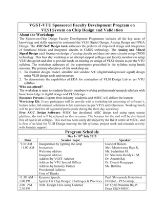
- 1. VGST-VTU Sponsored Faculty Development Program on VLSI System on Chip Design and Validation About the Workshop: The System-on-Chip Design Faculty Development Programme includes all the key areas of knowledge and skills required to command the VLSI Digital Design, Analog Design and FPGA Design. The ASIC/SoC Design track addresses the problem of chip-level design and integration of functional blocks and integrated circuits in CMOS technology. The Analog and Mixed Signal Design track focuses on design of analog circuits and data converter circuits using CMOS technology. This four day workshop is an attempt support colleges and faculty members to setup VLSI design lab and also to provide hands on training on design of VLSI circuits as per the VTU syllabus. The workshop addresses all the experiments prescribed in the syllabus using hands sessions. The primary objectives of this workshop are: 1. To illustrate design, model, simulate and validate SoC (digital/analog/mixed signal) design using VLSI design tools and resources 2. To demonstrate the capabilities of EDA for conduction of VLSI Design Lab as per VTU syllabus Who can attend? The workshop is open to students/faculty members/working professionals/research scholars with basic knowledge in digital design and VLSI design. Resource Persons: Experts from industry, academia and MSEC will deliver the lectures Workshop Kit: Every participant will be provide with a workshop kit consisting of software’s, lecture notes, lab manual, solutions to lab exercises (as per VTU) and references. Working lunch will be provided for all registered participants during the three day workshop. Free ASIC Design Software: MSEC has developed ASIC design tool using open source platform, the tool will be released on this occasion. The licenses for the tool will be distributed free of cost to all colleges. This tool has been solely developed by the R&D centre at MSEC, and is first of its kind for VLSI Design meeting the lab syllabus, project work and research activity with foundry support. Program Schedule Day 1- 10th July 2013 Time Session Topic Speaker 9.30 AM – 11.00 AM Inauguration by lighting the lamp Invocation Welcome address Inaugural address Address by VGST-Advisor Address by VTU Special Officer Address by Industry Partner Presidential Address Vote of Thanks Guest of Honors Shri. Muniswamy Raju K. Mr. Sudarshan M. Dr. Sreerama Reddy G. M. Dr. Ananth Raj Dr. Dinesh Rangappa Ms. Babitha 11.30 AM – 1.00 PM Keynote Speech: System On Chip Design: Challenges & Practices Prof. Shivananda Koteshwar Director – PES Group 2.00 PM – 2.30 PM ASIC Design Flow using Cadence Dr. Cyril Prasanna Raj P. Dean R&D-MSEC
- 2. Hands on Front End Design and Physical Design2.30 PM – 5.00 PM Digital Design of Complex Circuits using MOS Vinod Kumar Asst. Professor, MSEC Arun Alex Design Engineer, MSEC Day 2 – 11th July 2013 Sessions Topic Speaker 9.30 AM – 11.00 AM VLSI Design: Design Challenges and Road Map Dr. Bharadwaj Amrutur IISc., Bangalore 11.30 AM – 1.00 PM Design of OPAMP using 130nm/90nm CMOS Dr. Cyril Prasanna Raj P. Dean R&D-MSEC 2.00 PM – 2.30 PM Analog Circuit Design using Cadence Divya Dechamma Asst. Professor-MSEC 2.30 PM – 5.00 PM Hands on Analog Design Experiments Azrathamma Asst. Professor-MSEC Day 3 – 12th July 2013 Sessions Topic Speaker 9.30 AM – 11.00 AM Mixed Signal Design Challenges and Industry Practices Dr. Gaurab Banerjee Assistant Professor IISc., Bangalore 11.30 AM – 1.00 PM Design and Modeling of Data Converters Dr. Cyril Prasanna Raj P. Dean R&D-MSEC 2.00 PM – 2.30 PM Data Converter design using Cadence Divya Dechamma Asst. Professor-MSEC 2.30 PM – 5.00 PM Hands on session Azrathamma Asst. Professor-MSEC Day 4 – 13th July 2013 Sessions Topic Speaker 9.30 AM – 11.00 AM System On Chip Design Expert from Cadence 11.30 AM – 1.00 PM Layout Design and Verification Industry Experts 2.00 PM – 4.00 PM SoC Design and Validation Vinod Kumar Asst. Professor, MSEC Arun Alex Design Engineer, MSEC 4.00 PM – 4.30 PM Valedictory Function Theory Sessions: Seminar Hall, 2nd Floor Lab Sessions: VLSI Lab, 3rd Floor Lunch Break: 1.00 PM to 2.00 PM Tea Breaks: 11.00 AM – 11.30 AM and 3.15 PM – 3.30 PM Breakfast: 9.00 AM – 9.30 AM