
Recommended
More Related Content
What's hot
What's hot (20)
Similar to PE4MSc_Ch1_SC_devices.pptx
Similar to PE4MSc_Ch1_SC_devices.pptx (20)
Recently uploaded
Recently uploaded (20)
PE4MSc_Ch1_SC_devices.pptx
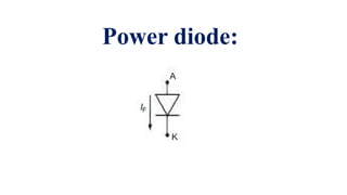
- 1. Power diode:
- 2. Symbol Power diode: is a two-terminal pn-junction device. The equivalent circuit and i-v curve are displayed as follows, where the diode conducts when a battery is connected across its terminals . P-N junction P-N junction 𝑰𝑫 = 𝑰𝒔 (𝒆 𝑽𝑫 𝒏𝑽𝒕 − 𝟏) where, VD = voltage across the diode Is = the reverse bias saturation current (or scale current), n=quality factor or emission coefficient Vt=KT/q=thermal voltage where, K =Boltzmann constant T= absolute temperature q=charged electron
- 3. • P-N junction is formed by alloying diffusion and epitaxial growth. • Modern techniques in diffusion and epitaxial processes permit desired device characteristics. • The diodes have the following advantages including: high mechanical and thermal reliability, high peak inverse voltage, low reverse current, low forward voltage drop, high efficiency and compactness. Power Diode:
- 4. Fig. static V- I characteristics of diode
- 5. Ideal diode characteristics Real diode characteristics vs
- 6. Ideal diode circuit symbol: Real diode circuit symbol: vs
- 7. Fig. Switching characteristics of diode OFF state ON state
- 8. Fig. Turn-Off Characteristics of Power Diode: a) Variation of Forward Current if ; b) Variation of Forward Voltage Drop vf ; c) Variation of Power Loss Significant power loss
- 9. Very common diode parameters are: Forward recovery time tFR is the time required for the diode voltage to drop to a particular value after the forward current starts to flow. Reverse recovery time trr is the time interval between the application of reverse voltage and the reverse current dropped to a particular value. • Parameter ta is the interval between the zero crossing of the diode current and when it becomes IRR. On the other hand, tb is the time interval from the maximum reverse recovery current to 0.25 of IRR . ta-due to storage charge in the depletion region tb- due to storage charge in the bulk resistance.
- 10. • The ratio of the two parameters ta and tb is known as the softness factor SF. • Diodes with abrupt recovery characteristics are used for high- frequency switching. • In practice, a design engineer frequently needs to calculate reverse recovery time in order to evaluate the possibility of high- frequency switching. • As a rule of thumb, the lower trr is, the faster the diode can be switched. 𝑡𝑟𝑟 = 𝑡𝑎 + 𝑡𝑏 If tb is negligible compared to ta (which commonly occurs), then the following expression is valid: 𝑡𝑟𝑟 = 2𝑄𝑟𝑟 𝑑𝑖/𝑑𝑡 how? Assignment
- 11. from which the reverse recovery current is 𝐼𝑟𝑟 = 𝑑𝑖 𝑑𝑡 2𝑄𝑟𝑟 how? Assignment where Qrr is the storage charge, and can be calculated from the area enclosed by the path of the recovery current.
- 12. During “Turn On” the instantaneous forward voltage drop across a diode may reach a level considerably higher than its steady state voltage drop for the given forward current. This is called forward recovery voltage. During “Turn Off” the diode current goes negative first before reducing to zero. This is called reverse recovery of a diode. The peak negative current flowing through a diode during Turn Off is called the “reverse recovery current” of the diode. The total time for which the diode current remains negative during Turn Off is called “the reverse recovery time” of the diode. In general
- 13. A diode can not block reverse voltage till the reverse current through the diode reaches its peak value. Both the “reverse recovery current” and the “reverse recovery time” of a diode depends on the forward current during Turn Off, rate of decrease of the forward current (di/dt) and the type of the diode. Normal or slow recovery diodes have smaller reverse recovery current but longer reverse recovery time. They are suitable for line frequency rectifier operation. Fast recovery diodes have faster switching times but comparatively lower break down voltages. They are suitable for high frequency rectifier or inverter free- wheeling operation. Fast recovery diodes need to be protected against voltage transients during Turn Off” using R-C snubber circuit.
- 14. Snubber circuit Snubber circuits are essential for diodes used in switching circuits. It can save a diode from overvoltage spikes, which may arise during the reverse recovery process. High power dissipation in the device A very common snubber circuit for a power diode consists of a capacitor and a resistor connected in parallel with the diode as shown in the fig. And the typical formulas Fig. A typical snubber circuit 𝑑𝑣 𝑑𝑡 = 0.632 ∗ 𝑉 𝑠 𝑅𝑠𝐶𝑠 𝑅𝑠 = 𝑉 𝑠 𝐼𝑅𝑅 and
- 15. Diodes Classification : Depending on the recovery characteristics, and manufacturing. 1. General - purpose diodes: they have high trr=25 µS and with frequency < 1kHz, applied in AC to DC circuits. The current rating reaches up to 1000A, and up to 5kV. 2. Fast recovery diodes: they have small trr=5 µS and with frequency < 5kHz, applied in DC to DC and DC to AC circuits. The current rating reaches up to 100A, and up to3kV. 3. Schottkey diode: they have approximately zero reverse recovery time with high frequency up to 10kHz, and applied in high current low voltage applications. The current rating reaches up to 300A and 100V circuit voltage.
- 16. Series –Connected Diodes : In high voltage DC applications (mainly), the diodes are connected in series with the purpose to increase the reverse blocking capabilities. The difference in the i-v curve in the reverse blocking condition occurs due to manufacturing errors and tolerances, therefore each diode should carry different voltage , while the leakage current is the same. The solution is to enforce equal voltage sharing across the diodes by connecting a sharing resistances as well shown below:
- 17. Rs 1 Rs 2 Rs 1 Rs 2 (Is 2 Is1) Rs1 V D 1 VD 2 VD 1 . Rs 2 Rs 1 Rs 2 VD 2 Rs 2 .(Is 2 Is1) c a se : V D 1 V D 2 Vs 2 Is1 VD 1 Is 2 VD 2 ; VD 1 VD 2 (Is 2 Is 1 ); Mathematical Modeling: Is1 Id 1 Is 2 Id 2 Vs VD 1 VD 2 VD 2 Vs VD 1
- 18. Parallel –Connected Diodes : In high power applications, diodes are connected in parallel with the purpose to increase the current carrying capability. Due to some differences in the Bulk resistances of both diodes, there is a different current will flow through the diodes. Therefore by connecting resistances in series with the diodes the diode voltage is shared equally as well shown below: The function of both Ls1 and Ls2 is to equally sharing the current under dynamic behaviors. When ID1 rises, the inductor voltage Ls1.d(Id1)/dt increases, and a corresponding voltage of opposite polarity is induced across inductor Ls2. This resulting low impedance in the circuit of D2, therefore shifting the current to flow through D2 path.
- 19. Mathematical Modeling: The following equations are derived under steady-state conditions VD1 V3 VD2 V4; VD1 Rs3.ID1 VD2 Rs4.ID2 Let Rs1 Rs2 R R(ID 2 ID1) VD1 VD2 R VD1 VD2 ID2 ID1
- 21. High forward current High reverse voltage Fast switching The three most desired characteristics of diode?
- 22. Example (R Load):-PSCAD software 100.0 [ohm] Vsource 240 kV, 50 Hz AC Source R=0 V HALF-WAVE RECTIFIER V v(t) = V*sin(theta) T LOAD V A Diode
- 23. Simulated results (half-wave rectifier):
- 24. A Simple Circuit (R-L Load) V A T v(t) = V*sin(theta) V HALF-WAVE RECTIFIER R=0 V 240 kV, 50 Hz AC Source Vsource LOAD 100 [ohm] Vd Ia Vdiode VL 1 [H]
- 25. • Current continues to flow for a while even after the input voltage has gone negative Vo,Is dependi ng on R,L Illustrated by PSCAD example! t1 t2 t3 t0
- 26. • Current continues to flow for a while even after the input voltage has gone negative For L=2H t1 t2 t3 t0
- 27. Voltage ripple reduction: V A T v(t) = V*sin(theta) V HALF-WAVE RECTIFIER R=0 V 240 kV, 50 Hz AC Source Vsource LOAD 100 [ohm] 1.0 [uF] Diode
- 28. Voltage ripple reduction: For 100 𝝁𝑭:
- 29. For 1000 𝝁𝑭:
- 30. V A v(t) = V*sin(theta) V FULL-WAVE RECTIFIER 240 kV, 50 Hz AC Source Vsource LOAD 100 [ohm] T T T T R=0 V Vlaod2
- 31. Simulated results (full-wave rectifire):
- 32. V A v(t) = V*sin(theta) V FULL-WAVE RECTIFIER 240 kV, 50 Hz AC Source Vsource THYRISTOR FIRING PULSE CONTROL CIRCUIT LOAD 100 [ohm] T T T T R=0 V Vlaod2 1000 [uF] Ia Voltage ripple reduction:
- 33. For 100 𝝁𝑭:
- 34. For 1000 𝝁𝑭:
- 35. Power Thyristor (SCR): Fig. Structure of thyristor Fig. Symbol of thyristor Fig. Equivalent circuit of thyristor Ig Ia A G K
- 36. Mode of Current Flow in a Thyristor: Reverse Blocking Mode Forward Blocking Mode Forward Conduction Mode
- 37. • The cathode is made positive with respect to anode by supplying voltage and keeping G open. • Here, Junctions J1 and J3 are reverse biased whereas the junction J2 is forward biased. • The behavior of the thyristor here is similar to that of two diodes are connected in series with reverse voltage applied across them. • As a result only a small leakage current of the order of a few μAmps flows. This is the reverse blocking mode or the off-state of the thyristor, (open circuit function). • If the reverse voltage is now increased, then at a particular voltage, known as the critical breakdown voltage VBR, an avalanche occurs at J1 and J3 and the reverse current increases rapidly. • A large current associated with VBR gives rise to more losses in the SCR, which results in heating of the thyristor. Reverse Blocking Mode :
- 38. Forward Blocking Mode: • Considering the figure:- • J1 and J3 are forward biased; but junction J2 goes into reverse biased. • The thyristor conducts currents from anode to cathode with a very small voltage drop across it. • A thyristor is brought from forward blocking mode to forward conduction mode by turning it on by exceeding the forward break over voltage or by applying a gate pulse between gate and cathode. • In this mode, thyristor is in on-state and behaves like a closed switch • Voltage drop across thyristor in the on state is of the order of 1 to 2 V depending beyond a certain point
- 39. • Considering the anode is positive with respect to the cathode, with gate kept in closed condition. • J1, J2 and J3 are forward biased • Once the thyristor is turned on, we can see from the diagram for characteristics of thyristor, it continues conduction. • In this mode of operation, the thyristor conducts maximum current with minimum voltage drop, this is known as the forward conduction or the turn-on mode of the thyristor, (closed circuit function) Forward Conduction Mode:
- 40. Forward Conduction… •The SCR can be brought back to the forward blocking state from the forward conduction state by reducing the anode or forward current below the holding current level.
- 41. Fig. static characteristics of Thyristor
- 42. Methods of Thyristor Turn-on Forward high voltage triggering Thermal triggering Light triggering Gate triggering... Very common dv/dt triggering
- 43. •An SCR is said to be ‘turned OFF’ if there is no flow of forward current and even if the SCR is once again forward biased (positive voltage at anode), the SCR will not conduct without any Gate Signal. •The reverse voltage, which causes to commutate the SCR, is called the Commutation Voltage. •The commutation methods are classified into two major types: Natural Commutation Forced Commutation Thyristor Turn-Off Methods
- 45. The transition of an SCR from forward conduction state to forward blocking state is called as turn OFF or commutation of SCR. Once the SCR starts conducting, the gate has no control over it to bring back to forward blocking or OFF state. To turn OFF the SCR, the current must be reduced to a level below the holding current of SCR. SCR turn OFF is achieved by reducing the forward current to zero. But if we apply the forward voltage immediately after the current zero of SCR, it starts conducting again even without gate triggering. This is due to the presence of charge carriers in the four layers. Therefore, it is necessary to apply the reverse voltage, over a finite time across the SCR to remove the charge carriers.
- 46. Hence the turn OFF time is defined as the time between the instant the anode current becomes zero and the instant at which the SCR retains the forward blocking capability. The excess charge carriers from the four layers must be removed to bring back the SCR to forward conduction mode. This process takes place in two stages. In a first stage excess carriers from outer layers are removed and in second stage excess carriers in the inner two layers are to be recombined. Hence, the total turn OFF time tq is divided into two intervals; reverse recovery time trr and gate recovery time tgr. • The figure above shows the switching characteristics of SCR during turn ON and OFF. • The time t1 to t3 is called as reverse recovery time; at the instant t1the anode current is zero and builds up in the reverse direction which is called as reverse recovery current.
- 47. • This current removes the excess charge carriers from outer layers during the time t1 to t3. • At instant t3, junctions J1 and J3 are able to block the reverse voltage but, the SCR is not yet able to block the forward voltage due to the presence of excess charge carriers in junction J2. • These carriers can be disappeared only by the way of recombination and this could be achieved by maintaining a reverse voltage across the SCR. Hence , during the time t3 to t4, the recombination of charges takes place and at the instant t4, junction J2 completely recovers. This time is called gate recovery time tgr. From the characteristics figure, the turn OFF time is the time interval between the t1 and t4. Generally, this time varies from 10 to 100𝜇𝑠𝑒𝑐.
- 48. This turn OFF time tq is applicable to the individual SCR. The time required by the commutation circuit to apply the reverse voltage to commutate the SCR is called the circuit turn OFF time (tc). For a safety margin or reliable commutation, this tc must be greater than the tq otherwise commutation failure occurs. The SCRs which have slow turn OFF time as in between 50 to 100𝜇𝑠𝑒𝑐 are called as converter grade SCRs. These are used in phase controlled rectifiers, cycloconverters, AC voltage regulators, etc. The SCRs which have fast turn OFF time as in between 3 to 50𝜇𝑠𝑒𝑐 are inverter grade SCRs. These are costlier compared to converter grade and are used in choppers, force commutated converters and inverters.
- 49. • Single-phase half-wave SCR controlled rectifier with a firing angle of α Firing or triggering of SCR V0
- 50. Firing angle(α) Firing angle(α): is an angle at which the SCR is triggered or fired, and measured with respect to the zero crossing point of the mains that supply the rectifier after which the SCR becomes forward bias. It is also called triggering angle.
- 51. Thyristor based halfwave rectifier _ PSCAD V A T 2 v(t) = V*sin(theta) V HALF-WAVE RECTIFIER R=0 V 240 kV, 50 Hz AC Source Vsource Diode GP 10 [ohm]
- 52. At 300 firing angle α
- 53. 300 firing angle 900 firing angle 1500 firing angle 1800 firing angle
- 54. 𝛽 α • Extinction angle(𝜸): It is the angle at which the SCR gets turned off. For AC resistive load applications normally, the commutation takes place at every zero crossings. • In RL load application it will vary irrespective of zero crossing Conduction angle (𝜷): an angle that measures the SCR period of conduction (how long it conducts in one cycle of time). This angle depends on the firing angle α and the load impedance angle φ . For purely resistive load, the conduction angle β = (π- α ).
- 55. when the load contain inductor: α 𝛽
- 56. 𝑅𝑀𝑆 𝑙𝑜𝑎𝑑 𝑣𝑜𝑙𝑡𝑎𝑔𝑒, 𝑉0 𝑉0 = 𝛼 2𝜋 𝑉𝑚𝑠𝑖𝑛 𝜔𝑡 2 𝑑(𝜔𝑡) = 𝑉𝑚 2 1 𝜋 { 2𝜋 − 𝛼 + 𝑠𝑖𝑛𝛼 2 }
- 57. SCR based three-phase rectification: PSCAD V A T 2 v(t) = V*sin(theta) 240 kV, 50 Hz AC Source Vsourcea FP1 THYRISTORs with FIRING PULSES T 2 T 2 FP2 FP3 10 [ohm] A B C Vsourceb Vsourcec Io T 2 T 2 T 2 FP1 FP2 FP3 Load Vo 1 3 5 2 6 4
- 58. 𝐅𝐢𝐫𝐢𝐧𝐠 𝐚𝐧𝐠𝐥𝐞𝐬 𝐟𝐨𝐫 𝟎 ≤ 𝜶 ≤ 𝟑𝟎0
- 61. Beyond 1200 firing angle, proper triggering of the whole valves fails; i.e., commutation failure 1300 firing angle 1750 firing angle Thus, it demands robust control system
- 62. Commutation failure • Commutation failure is a common fault of converters. • It is the failure of an incoming valve (due to insufficient extinction angle) to take the control of load current when commutating voltage reverses its polarity. • During the operation of inverters, when the time (angle γ) of applying negative voltage on the valve that has just been turned off is shorter than the time required for it to restore the blocking capability and the valve is conducted again when positive voltage is applied, commutation failure of the converter valve would occur. • The causes might be: Low AC side voltage (for example due to fault) Late of firing angle( experiences phase shift ) or the DC current increases, Thus the angle extinction angle γ would be decreased.
- 63. 𝛾 = 𝑒𝑥𝑡𝑖𝑛𝑖𝑐𝑡𝑖𝑜𝑛 𝑎𝑛𝑔𝑙𝑒 𝛽 = 𝑐𝑜𝑛𝑑𝑢𝑐𝑡𝑖𝑜𝑛 𝑎𝑛𝑔𝑙𝑒 𝜇 = 𝑜𝑣𝑒𝑟𝑙𝑎𝑝 𝑎𝑛𝑔𝑙𝑒
- 64. • Fig. 1 shows the basic equivalent circuit of line commutated six pulse bridge converter. • Under normal circumstances, commutation process between valve 1 and valve 3 is illustrated in Fig. 2, when the valve 3 is fired, valve1 is forced to a negative bias and get switched off for a certain period of time after the extinction of its current (denoted by the extinction angle 𝛾), and if the valve become positively biased before complete switch off occurs, this thyristor will regain current and it will increase the risk of commutation failure.
- 65. •Additively, in the HVDC inverter station, the firing angle is large (around 1300-1400), that's why the inverter is more prone to commutation failure compared to rectifier which is rarely fails to commutate because its firing angle is less than 900. •For proper operation of valves during commutation, extinction angle 𝛾 must be at a minimum value and it is expressed as: 𝛾 = 1800 − 𝛼 − 𝜇
- 66. Gate Turn-Off Thyristor (GTO): A gate turn-off thyristor (GTO) is a special type of thyristor. GTOs, are fully controllable switches which can be turned on and off by switching the polarity of the gate signal. • Turn on is accomplished by a "positive current" pulse between the gate and cathode terminals. • Turn off is accomplished by a "negative current" pulse between the gate and cathode terminals.
- 67. Slow switching speeds. Used at very high power levels. Requires elaborate gate control circuitry (needs a turn-off snubber circuit).
- 68. GTO… cont’d IV-Characteristics of GTO (a) Symbol of GTO (b) Equivalent circuit of GTO
- 69. Dynamics Characteristics of GTO
- 70. GTO: Characteristic Description Thyristor (1600 V, 350 A) GTO (1600 V, 350 A) VT on On-state voltage drop 1.5 V 3.4 V ton, Ig on Turn-on time, gate current 8 µs, 200 mA 2 µs, 2 A toff Turn-off time 150 µs 15 µs Comparison of an SCR and GTO of same rating GTO and SCR are pulse triggering devices
- 71. IGBT: MOSFET: BJT: These all are level triggering devices
- 72. Comparing IGBT with BJT and MOSFET: Characteristic Power BJT Power MOSFET IGBT Voltage Rating High < 1kV High < 1kV Very High > 1kV Current Rating High < 500 A Low < 200 A Very High > 500 A Input Parameter Base Current, Ib Voltage, VGS Voltage, VGE Input Drive Current gain (hfe) 20-200 Voltage, VGS 3-10V Voltage, VGE 4-8V Input Drive Power High Low Low Input Drive Circuitry Complex Simple Simple Input Impedance Low High High Output Impedance Low Medium Low Switching Loss High Low Medium Switching Speed Low Fast Medium
- 73. Bipolar Junction Transistor (BJT) A BJT is a current-controlled switch that can be considered as two diodes with a shared anode. A sufficiently large base current results in the device fully on (iB > IC/hFE, where hFE is the dc current gain). The base current must be supplied continuously to keep the switch turned on. Used commonly in the past (now used in specific applications). Being replaced by MOSFETs and IGBTs.
- 74. Metal-Oxide-Semiconductor Field Effect Transistor (MOSFET) A MOSFET (type of FET) is a voltage-controlled device - easy to control. It uses an electric field to control the shape and hence the conductivity of a channel of majority-charge- carriers in a semiconductor material. MOSFETS have gate, drain, and source terminals that correspond roughly to the base, collector, and emitter of BJTs. MOSFETs also have a fourth terminal called the body, base, bulk, or substrate. Optimal for low-voltage operation at high switching frequencies. On-state requires continuous application of gate-source voltage of appropriate magnitude
- 75. Like the BJT, the IGBT has a small on-state voltage. Similar to the GTO, IGBT can be designed to block negative voltage. Its name also implies the fusion between them. “Insulated Gate” refers to the input part of MOSFET having very high input impedance. It does not draw any input current rather it operates on the voltage at its gate terminal. IGBT Advantages over MOSFET, BJT and GTO: It is a voltage controlled device Similar to the MOSFET, the IGBT has a high impedance gate, thus requires only a small amount of energy to switch the device.
- 76. Typical switching characteristics IGBT characteristics:
- 78. Operation principle: The two terminals of IGBT collector (C) and emitter (E) are used for the conduction of current while the gate (G) is used for controlling the IGBT. Its operation is based on the biasing between Gate-Emitter terminals and Collector-Emitter terminals. The collector-emitter is connected to Vcc such that the collector is kept at a positive voltage than the emitter. The junction j1 becomes forward biased and j2 becomes reverse biased. At this point, there is no voltage at the gate. Due to reverse bias of j2, the IGBT remains switched off and no current will flow between collector and emitter.
- 79. Applying a gate voltage VG positive than the emitter, negative charges will accumulate right beneath the SiO2 layer due to capacitance. Increasing the VG elevates the number of charges which eventually form a layer when the VG exceeds the threshold voltage, in the upper P-region. This layer form N- channel that shorts N- drift region and N+ region. The electrons from the emitter flow from N+ region into N- drift region. While the holes from the collector are injected from the P+ region into the N- drift region. Due to the excess of both electrons and holes in the drift region, its conductivity increase and starts the conduction of current. Hence the IGBT switches ON. Therefore, IGBT gets turned ON and begins to conduct forward current IC.
- 80. Example: V A 2 T v(t) = V*sin(theta) V HALF-WAVE RECTIFIER R=0 V 240 kV, 50 Hz AC Source Vsource Diode GP 10 [ohm] IGBT based halfwave rectifier _ PSCAD
- 81. Triggered at 300
- 82. If the pulse duration is increased by 0.002sec
- 83. In general, once again the applications of PE devices:
Editor's Notes
- Bulk resistance is the approximate resistance across the terminals of the diode when a forward voltage and current are applied across the diode