SlideShare une entreprise Scribd logo
1  sur  6
Télécharger pour lire hors ligne
3.1.8-Electrical to Optical conversion

In the optical communication systems, the desired signal travels in an optical form. But the
source produces an electrical signal.

So, there is a need to convert this electrical signal to the optical form so the optical
communication system can handle with it.

There are some modulation techniques to make this conversation, and in our project we used
the direct intensity modulation.

3.1.8.1-Intensity Modulation (IM):

In optical communications, intensity modulation (IM) is a form of modulation in which the
optical power output of a source is varied in accordance with some characteristic of the
modulating signal.


                             Figure-3.1.8.1.1 Current & Optical Power

In intensity modulation, there are no discrete upper and lower sidebands in the usually
understood sense of these terms, because present optical sources lack sufficient coherence to
produce them.
3.1.8.2-Electrical to Optical circuit:
The circuit which is responsible to do the intensity modulation is actually composed of two
parts (buffer and driver) coupled to each other in series.


3.1.8.2.1-Common Collector (Buffer Amplifier):

Figure(3.1.8.2.1) is the schematic diagram of a buffer amplifier. This circuit is a common-
collector amplifier. A common-collector amplifier has high input impedance and low output
impedance. Since the input of summing circuit is connected to the high impedance of the
common-collector amplifier, the buffer has little effect on the operation of the summing
circuit. The output of the common-collector buffer is then connected to an external load;
therefore, the changes in the output load cannot reflect back to the oscillator circuit. Thus,
the buffer amplifier reduces interaction between the load and the summing circuit.


                                 Figure-3.1.8.2.1 Buffer Schematic
Components List:
                                   ITEM              NEEDED
                                   R3=1kΩ                    1
                                   R1=R2=5kΩ                 2
                                   Q1-2SC2570                1
                                   C1=0.1µf                  1
                                   C2=1µf                    1
                                         Table-(3.1.8.2.1)
3.1.8.2.2-Common Emitter (Driver Circuit):
In electronics, a common-emitter amplifier is one of three basic single-stage bipolar-
junction-transistor (BJT) amplifier topologies, typically used as a voltage amplifier. In this
circuit the base terminal of the transistor serves as the input, the collector is the output, and
the emitter is common to both (for example, it may be tied to ground reference or a power
supply rail), hence its name. The analogous field-effect transistor circuit is the common-
source amplifier.


                 Figure-(3.1.8.2.2.1)                              Figure-(3.1.8.2.2.2)
                     Basic NPN                                      Adding an emitter
               common-emitter circuit                               resistor decreases
             (neglecting biasing details).                          gain, but increases
                                                                       linearity and
                                                                         stability


In our project we used the common-emitter-with a resistance amplifier (Figure-3.1.8.2.2.3) to
drive the optical source and convert the signal from the electrical form into optical form
using the intensity modulation.


                               Figure-3.1.8.2.2.3 Driver Circuit Schematic
As shown in figure-(3.1.8.2.2.3), there is a coupling capacitors (C3,C4) in series between the
Buffer and the Driver circuits,


Components List:
                                  ITEM                        NEEDED
                                  R6=47Ω                           1
                                  R4=5kΩ                           1
                                  R5=4.5kΩ                         1
                                  Q2-2SC1959                       1
                                  C4=47µ                           1
                                  C3=0.1µ                          1
                                  Optical-Tx (HFBR1414)            1
                                             Table-(3.1.8.2.2)


By coupling the two circuits (Buffer & Driver) to each other in series we’ve got the electrical
to optical circuit as shown in figure-(3.1.8.2.2.4).


                                            Figure-(3.1.8.2.2.4)
                                  Electrical to Optical circuit schematic
3.1.8.2.3-DC Analysis:
From the values in table-(3.1.8.2.2),
R6=47Ω, R4=5kΩ, R5=4.5kΩ, Vcc=9volts.


                                                   Figure-(3.1.8.2.2.3)


Thevenin's resistor equivalent (Rth) and voltage equivalent (Vth) have to be found first.


Rth =         ,           Rth =                = 2.368kΩ


Vth =         =                   = 4.264 volts


Once these two values have been found, the base current (IB) can be found.


IB =      (       )
                      =              (     )
                                                   = 5 × 10⁻⁴ Ampers


IC = β.IB ,                        IE = IC + IB,
IC = 50 mA,                        IE = 50.5 mA,
3.1.8.2.4-Capacitor Coupling (CR-coupling):


Why using coupling capacitors?
Sections of electronic circuits may be linked with a capacitor because capacitors pass AC
(changing) signals but block DC (steady) signals. This is called capacitor coupling or CR-
coupling.


                                       Figure-(3.1.8.2.4)


For successful capacitor coupling, the signals must pass through with little or no distortion.
This is achieved if the time constant (RC) is larger than the time period (T) of the lowest
frequency audio signals required (typically 20Hz, T = 50ms).

Contenu connexe

Tendances

Tendances (20)

OFC
OFCOFC
OFC
 
Chapter 3b
Chapter 3bChapter 3b
Chapter 3b
 
Modulation of light
Modulation of lightModulation of light
Modulation of light
 
Electro-optic Modulator
Electro-optic ModulatorElectro-optic Modulator
Electro-optic Modulator
 
Photonic Integrated Circuit Technology
Photonic Integrated Circuit TechnologyPhotonic Integrated Circuit Technology
Photonic Integrated Circuit Technology
 
Optical switching
Optical switchingOptical switching
Optical switching
 
Optical fibres
Optical fibresOptical fibres
Optical fibres
 
Optical fiber communication || History and working principle || Yaman Shrestha
Optical fiber communication || History and working principle || Yaman ShresthaOptical fiber communication || History and working principle || Yaman Shrestha
Optical fiber communication || History and working principle || Yaman Shrestha
 
Photo detector noise
Photo detector noisePhoto detector noise
Photo detector noise
 
Photonics Metamaterials
Photonics MetamaterialsPhotonics Metamaterials
Photonics Metamaterials
 
Introduction to how fiber optics work
Introduction to how fiber optics workIntroduction to how fiber optics work
Introduction to how fiber optics work
 
A brief description of photolithography
A brief description of photolithographyA brief description of photolithography
A brief description of photolithography
 
Chapter 5b
Chapter 5bChapter 5b
Chapter 5b
 
Impedance Matching
Impedance MatchingImpedance Matching
Impedance Matching
 
Ppt
PptPpt
Ppt
 
Electro-optic modulators
Electro-optic modulatorsElectro-optic modulators
Electro-optic modulators
 
Optical Fibre Splices , Couplers and Connectors
Optical Fibre Splices , Couplers and ConnectorsOptical Fibre Splices , Couplers and Connectors
Optical Fibre Splices , Couplers and Connectors
 
Erbium Doped Fiber Amplifier (EDFA)
Erbium Doped Fiber Amplifier (EDFA)Erbium Doped Fiber Amplifier (EDFA)
Erbium Doped Fiber Amplifier (EDFA)
 
Introduction to Optical Detector
Introduction to Optical DetectorIntroduction to Optical Detector
Introduction to Optical Detector
 
Molecular electronic devices
Molecular electronic devicesMolecular electronic devices
Molecular electronic devices
 

Similaire à Electrical to optical conversion final

chapter_1_per_unit_power system_august_2011.ppt
chapter_1_per_unit_power system_august_2011.pptchapter_1_per_unit_power system_august_2011.ppt
chapter_1_per_unit_power system_august_2011.pptRachmadi8
 
Design, Simulation and Implementation of Flyback based, True Single Stage, Is...
Design, Simulation and Implementation of Flyback based, True Single Stage, Is...Design, Simulation and Implementation of Flyback based, True Single Stage, Is...
Design, Simulation and Implementation of Flyback based, True Single Stage, Is...IJMER
 
Comparative Evaluation of Three Phase Three Level Neutral Point Clamped Z-So...
Comparative Evaluation of Three Phase Three Level  Neutral Point Clamped Z-So...Comparative Evaluation of Three Phase Three Level  Neutral Point Clamped Z-So...
Comparative Evaluation of Three Phase Three Level Neutral Point Clamped Z-So...NAGARAJARAOS
 
Physica curckts
Physica curcktsPhysica curckts
Physica curckts12B-129-El
 
Modeling and analysis of pfc with appreciable voltage ripple to achieve fast ...
Modeling and analysis of pfc with appreciable voltage ripple to achieve fast ...Modeling and analysis of pfc with appreciable voltage ripple to achieve fast ...
Modeling and analysis of pfc with appreciable voltage ripple to achieve fast ...Alexander Decker
 
Iaetsd a transformerless single-stage
Iaetsd a transformerless single-stageIaetsd a transformerless single-stage
Iaetsd a transformerless single-stageIaetsd Iaetsd
 
Real Analog - Circuits 1Chapter 1 Lab WorksheetsReal Analog – .docx
Real Analog - Circuits 1Chapter 1 Lab WorksheetsReal Analog –  .docxReal Analog - Circuits 1Chapter 1 Lab WorksheetsReal Analog –  .docx
Real Analog - Circuits 1Chapter 1 Lab WorksheetsReal Analog – .docxcatheryncouper
 
Modelling of fuzzy logic controller for variable step mppt in photovoltaic sy...
Modelling of fuzzy logic controller for variable step mppt in photovoltaic sy...Modelling of fuzzy logic controller for variable step mppt in photovoltaic sy...
Modelling of fuzzy logic controller for variable step mppt in photovoltaic sy...eSAT Journals
 
Analysis of 1MHz Class-E Power Amplifier for Load and Duty Cycle Variations
Analysis of 1MHz Class-E Power Amplifier for Load and Duty Cycle VariationsAnalysis of 1MHz Class-E Power Amplifier for Load and Duty Cycle Variations
Analysis of 1MHz Class-E Power Amplifier for Load and Duty Cycle VariationsIJPEDS-IAES
 
Tutorial simulations-elec 380
Tutorial simulations-elec 380Tutorial simulations-elec 380
Tutorial simulations-elec 380Moez Ansary
 
Design and Implementation of Single Phase AC-DC Buck-Boost Converter for Powe...
Design and Implementation of Single Phase AC-DC Buck-Boost Converter for Powe...Design and Implementation of Single Phase AC-DC Buck-Boost Converter for Powe...
Design and Implementation of Single Phase AC-DC Buck-Boost Converter for Powe...IJPEDS-IAES
 
Reach and Operating Time Correction of Digital Distance Relay
Reach and Operating Time Correction of Digital Distance Relay Reach and Operating Time Correction of Digital Distance Relay
Reach and Operating Time Correction of Digital Distance Relay Yayah Zakaria
 
Reach and Operating Time Correction of Digital Distance Relay
Reach and Operating Time Correction of Digital Distance Relay Reach and Operating Time Correction of Digital Distance Relay
Reach and Operating Time Correction of Digital Distance Relay IJECEIAES
 
EE375 Electronics 1: lab 3
EE375   Electronics 1: lab 3EE375   Electronics 1: lab 3
EE375 Electronics 1: lab 3Loren Schwappach
 
IRJET- Design and Implementation of Isolated Multi-Output Flyback Converter
IRJET- Design and Implementation of Isolated Multi-Output Flyback ConverterIRJET- Design and Implementation of Isolated Multi-Output Flyback Converter
IRJET- Design and Implementation of Isolated Multi-Output Flyback ConverterIRJET Journal
 
Soft Switched Multi-Output Flyback Converter with Voltage Doubler
Soft Switched Multi-Output Flyback Converter with Voltage DoublerSoft Switched Multi-Output Flyback Converter with Voltage Doubler
Soft Switched Multi-Output Flyback Converter with Voltage DoublerIJPEDS-IAES
 
Fuzzy logic based MPPT technique for a single phase Grid connected PV system ...
Fuzzy logic based MPPT technique for a single phase Grid connected PV system ...Fuzzy logic based MPPT technique for a single phase Grid connected PV system ...
Fuzzy logic based MPPT technique for a single phase Grid connected PV system ...THOKALA SOWMYA
 

Similaire à Electrical to optical conversion final (20)

chapter_1_per_unit_power system_august_2011.ppt
chapter_1_per_unit_power system_august_2011.pptchapter_1_per_unit_power system_august_2011.ppt
chapter_1_per_unit_power system_august_2011.ppt
 
Design, Simulation and Implementation of Flyback based, True Single Stage, Is...
Design, Simulation and Implementation of Flyback based, True Single Stage, Is...Design, Simulation and Implementation of Flyback based, True Single Stage, Is...
Design, Simulation and Implementation of Flyback based, True Single Stage, Is...
 
Comparative Evaluation of Three Phase Three Level Neutral Point Clamped Z-So...
Comparative Evaluation of Three Phase Three Level  Neutral Point Clamped Z-So...Comparative Evaluation of Three Phase Three Level  Neutral Point Clamped Z-So...
Comparative Evaluation of Three Phase Three Level Neutral Point Clamped Z-So...
 
Physica curckts
Physica curcktsPhysica curckts
Physica curckts
 
Modeling and analysis of pfc with appreciable voltage ripple to achieve fast ...
Modeling and analysis of pfc with appreciable voltage ripple to achieve fast ...Modeling and analysis of pfc with appreciable voltage ripple to achieve fast ...
Modeling and analysis of pfc with appreciable voltage ripple to achieve fast ...
 
Iaetsd a transformerless single-stage
Iaetsd a transformerless single-stageIaetsd a transformerless single-stage
Iaetsd a transformerless single-stage
 
The new approach minimizes harmonics in a single-phase three-level NPC 400 Hz...
The new approach minimizes harmonics in a single-phase three-level NPC 400 Hz...The new approach minimizes harmonics in a single-phase three-level NPC 400 Hz...
The new approach minimizes harmonics in a single-phase three-level NPC 400 Hz...
 
Real Analog - Circuits 1Chapter 1 Lab WorksheetsReal Analog – .docx
Real Analog - Circuits 1Chapter 1 Lab WorksheetsReal Analog –  .docxReal Analog - Circuits 1Chapter 1 Lab WorksheetsReal Analog –  .docx
Real Analog - Circuits 1Chapter 1 Lab WorksheetsReal Analog – .docx
 
Ijetcas14 641
Ijetcas14 641Ijetcas14 641
Ijetcas14 641
 
Modelling of fuzzy logic controller for variable step mppt in photovoltaic sy...
Modelling of fuzzy logic controller for variable step mppt in photovoltaic sy...Modelling of fuzzy logic controller for variable step mppt in photovoltaic sy...
Modelling of fuzzy logic controller for variable step mppt in photovoltaic sy...
 
Analysis of 1MHz Class-E Power Amplifier for Load and Duty Cycle Variations
Analysis of 1MHz Class-E Power Amplifier for Load and Duty Cycle VariationsAnalysis of 1MHz Class-E Power Amplifier for Load and Duty Cycle Variations
Analysis of 1MHz Class-E Power Amplifier for Load and Duty Cycle Variations
 
Tutorial simulations-elec 380
Tutorial simulations-elec 380Tutorial simulations-elec 380
Tutorial simulations-elec 380
 
Design and Implementation of Single Phase AC-DC Buck-Boost Converter for Powe...
Design and Implementation of Single Phase AC-DC Buck-Boost Converter for Powe...Design and Implementation of Single Phase AC-DC Buck-Boost Converter for Powe...
Design and Implementation of Single Phase AC-DC Buck-Boost Converter for Powe...
 
Reach and Operating Time Correction of Digital Distance Relay
Reach and Operating Time Correction of Digital Distance Relay Reach and Operating Time Correction of Digital Distance Relay
Reach and Operating Time Correction of Digital Distance Relay
 
Reach and Operating Time Correction of Digital Distance Relay
Reach and Operating Time Correction of Digital Distance Relay Reach and Operating Time Correction of Digital Distance Relay
Reach and Operating Time Correction of Digital Distance Relay
 
EE375 Electronics 1: lab 3
EE375   Electronics 1: lab 3EE375   Electronics 1: lab 3
EE375 Electronics 1: lab 3
 
IRJET- Design and Implementation of Isolated Multi-Output Flyback Converter
IRJET- Design and Implementation of Isolated Multi-Output Flyback ConverterIRJET- Design and Implementation of Isolated Multi-Output Flyback Converter
IRJET- Design and Implementation of Isolated Multi-Output Flyback Converter
 
Soft Switched Multi-Output Flyback Converter with Voltage Doubler
Soft Switched Multi-Output Flyback Converter with Voltage DoublerSoft Switched Multi-Output Flyback Converter with Voltage Doubler
Soft Switched Multi-Output Flyback Converter with Voltage Doubler
 
Fuzzy logic based MPPT technique for a single phase Grid connected PV system ...
Fuzzy logic based MPPT technique for a single phase Grid connected PV system ...Fuzzy logic based MPPT technique for a single phase Grid connected PV system ...
Fuzzy logic based MPPT technique for a single phase Grid connected PV system ...
 
15 47-58
15 47-5815 47-58
15 47-58
 

Electrical to optical conversion final

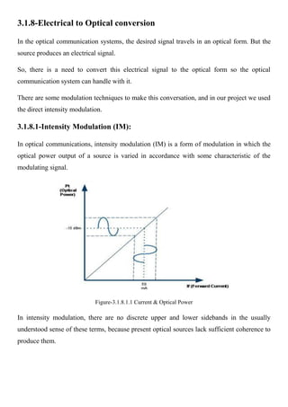
  • 1. 3.1.8-Electrical to Optical conversion In the optical communication systems, the desired signal travels in an optical form. But the source produces an electrical signal. So, there is a need to convert this electrical signal to the optical form so the optical communication system can handle with it. There are some modulation techniques to make this conversation, and in our project we used the direct intensity modulation. 3.1.8.1-Intensity Modulation (IM): In optical communications, intensity modulation (IM) is a form of modulation in which the optical power output of a source is varied in accordance with some characteristic of the modulating signal. Figure-3.1.8.1.1 Current & Optical Power In intensity modulation, there are no discrete upper and lower sidebands in the usually understood sense of these terms, because present optical sources lack sufficient coherence to produce them.
  • 2. 3.1.8.2-Electrical to Optical circuit: The circuit which is responsible to do the intensity modulation is actually composed of two parts (buffer and driver) coupled to each other in series. 3.1.8.2.1-Common Collector (Buffer Amplifier): Figure(3.1.8.2.1) is the schematic diagram of a buffer amplifier. This circuit is a common- collector amplifier. A common-collector amplifier has high input impedance and low output impedance. Since the input of summing circuit is connected to the high impedance of the common-collector amplifier, the buffer has little effect on the operation of the summing circuit. The output of the common-collector buffer is then connected to an external load; therefore, the changes in the output load cannot reflect back to the oscillator circuit. Thus, the buffer amplifier reduces interaction between the load and the summing circuit. Figure-3.1.8.2.1 Buffer Schematic Components List: ITEM NEEDED R3=1kΩ 1 R1=R2=5kΩ 2 Q1-2SC2570 1 C1=0.1µf 1 C2=1µf 1 Table-(3.1.8.2.1)
  • 3. 3.1.8.2.2-Common Emitter (Driver Circuit): In electronics, a common-emitter amplifier is one of three basic single-stage bipolar- junction-transistor (BJT) amplifier topologies, typically used as a voltage amplifier. In this circuit the base terminal of the transistor serves as the input, the collector is the output, and the emitter is common to both (for example, it may be tied to ground reference or a power supply rail), hence its name. The analogous field-effect transistor circuit is the common- source amplifier. Figure-(3.1.8.2.2.1) Figure-(3.1.8.2.2.2) Basic NPN Adding an emitter common-emitter circuit resistor decreases (neglecting biasing details). gain, but increases linearity and stability In our project we used the common-emitter-with a resistance amplifier (Figure-3.1.8.2.2.3) to drive the optical source and convert the signal from the electrical form into optical form using the intensity modulation. Figure-3.1.8.2.2.3 Driver Circuit Schematic
  • 4. As shown in figure-(3.1.8.2.2.3), there is a coupling capacitors (C3,C4) in series between the Buffer and the Driver circuits, Components List: ITEM NEEDED R6=47Ω 1 R4=5kΩ 1 R5=4.5kΩ 1 Q2-2SC1959 1 C4=47µ 1 C3=0.1µ 1 Optical-Tx (HFBR1414) 1 Table-(3.1.8.2.2) By coupling the two circuits (Buffer & Driver) to each other in series we’ve got the electrical to optical circuit as shown in figure-(3.1.8.2.2.4). Figure-(3.1.8.2.2.4) Electrical to Optical circuit schematic
  • 5. 3.1.8.2.3-DC Analysis: From the values in table-(3.1.8.2.2), R6=47Ω, R4=5kΩ, R5=4.5kΩ, Vcc=9volts. Figure-(3.1.8.2.2.3) Thevenin's resistor equivalent (Rth) and voltage equivalent (Vth) have to be found first. Rth = , Rth = = 2.368kΩ Vth = = = 4.264 volts Once these two values have been found, the base current (IB) can be found. IB = ( ) = ( ) = 5 × 10⁻⁴ Ampers IC = β.IB , IE = IC + IB, IC = 50 mA, IE = 50.5 mA,
  • 6. 3.1.8.2.4-Capacitor Coupling (CR-coupling): Why using coupling capacitors? Sections of electronic circuits may be linked with a capacitor because capacitors pass AC (changing) signals but block DC (steady) signals. This is called capacitor coupling or CR- coupling. Figure-(3.1.8.2.4) For successful capacitor coupling, the signals must pass through with little or no distortion. This is achieved if the time constant (RC) is larger than the time period (T) of the lowest frequency audio signals required (typically 20Hz, T = 50ms).