SlideShare une entreprise Scribd logo
1  sur  18
THE p-n JUNCTION

Structure of p-n Junction Diode:


p-n Junction Diode Fabrication:

   1. Ion Implantation Process
   2. Diffusion process
Figure 1 (c)Planar p-n junction diode fabrication on epitaxial substrate by diffusion,
(b) Planar p-n junction diode fabrication on epitaxial substrate by ion implantation.


Ion Implantation System
p-n Junction Diode Physics


Space Charge Region: The net positively and negatively charge region shown in
Figure 7.2 is called space charge region.
Built-in Voltage (Potential) Barrier (Vbi):

   •   Assume that no voltage bias is applied across the p-n junction barrier.

   •   So the p-n junction is in the thermal equilibrium- the Fermi level is constant
       throughout the system.

   •   The conduction band and valency band energies must bend in the space
       charge region to accommodate the carriers.

   •   The energy separation between the conduction bands in p- and n-type
       semiconductor is the built-in voltage Vbi.


   The built-in voltage can be found from the energy separation of intrinsic Fermi
   level in p- and n-regions. We can define the potentials ΦFn and ΦFp.
Electric Field: An electric field is created in the space charge region by the
separation of positive and negative charges. We will assume that the space charge
region abruptly ends in the n-region at x = +xn and abruptly ends in the p-region at
x = - xp (xp is a positive quantity).
E


Figure 7.5 is a plot of the electric field in the space charge region. The electric
field direction is from the n to the p-region or in the negative x direction for this
geometry.
Where C1 = constant of integration,

The potential is equal zero at x = -xp

The constant of integration is found as:
Space Charge Width:

The space charge region extends into the p- and n- regions from the metallurgical
junction. The space charge region can be defined using Equation (7.17) as:
Comparative Study of Space Charge for Various Bias Condition

                                F. Biasing         R. Biasing


Barrier potential Height           BPH: Vbi - Vf    BPH: Vbi+VR
(BPH): Vbi (Vo)            Vf = F. Biasing          VR = R. Biasing
Space Charge Width and Electric Field:

Figure 7.8 shows a p-n junction with an applied reverse-bias voltage VR. The
electric field in the space charge region and the applied electric field Eapp are
induced by the applied electric field.

                                       E


   •   At the edge of depletion region (space charge region) at xn and xp, the
       electric field is almost zero.

   •   Therefore, the electric field at the neutral zone is zero.

   •   The direction of the electric field from n-regions (+ve charge) to p-region
       (-ve) charge.
The total space charge width can be expressed as:
Home Work Problem:
JUNCTION CAPACITANCE:

Since a separation of positive and negative charges is existing, a capacitance is associated
in the p-n junction. The charge densities are changing with variation of R. biasing VR to
dVR. The junction capacitance can be expressed as:


       The space charge width under R. Biasing
ONE SIDED ABRUPT JUNCTION:
Home Work:

Contenu connexe

Tendances

[FULL ANIMATED(Download to view)] Unbiased diode, Forward biased , reverse bi...
[FULL ANIMATED(Download to view)] Unbiased diode, Forward biased , reverse bi...[FULL ANIMATED(Download to view)] Unbiased diode, Forward biased , reverse bi...
[FULL ANIMATED(Download to view)] Unbiased diode, Forward biased , reverse bi...Pratik Nakrani
 
P n junction characteristics
P n junction characteristicsP n junction characteristics
P n junction characteristicsAshvani Shukla
 
P n junction diode
P n junction diodeP n junction diode
P n junction diodeHarsh Vijay
 
Semiconductor diode
Semiconductor diodeSemiconductor diode
Semiconductor diodeRAMPRAKASHT1
 
Ete411 Lec11
Ete411 Lec11Ete411 Lec11
Ete411 Lec11mashiur
 
Pn diode presentation
Pn diode presentationPn diode presentation
Pn diode presentationBilawal Fiaz
 
Analog Electronics presentation on p-n junction diode
Analog Electronics presentation on p-n junction diodeAnalog Electronics presentation on p-n junction diode
Analog Electronics presentation on p-n junction diodeVipin Kumar
 
The p n Junction Diode (Basic Electronics)
The p n Junction Diode (Basic Electronics) The p n Junction Diode (Basic Electronics)
The p n Junction Diode (Basic Electronics) Ivan Saguit
 
Analog Electronics ppt on Transition & diffusion capacitance by Being topper
Analog Electronics  ppt on Transition & diffusion capacitance by Being topperAnalog Electronics  ppt on Transition & diffusion capacitance by Being topper
Analog Electronics ppt on Transition & diffusion capacitance by Being topperVipin Kumar
 
Diode and its Applications
Diode and its Applications Diode and its Applications
Diode and its Applications Prakash Rao
 
Semiconductor diodes1
Semiconductor diodes1Semiconductor diodes1
Semiconductor diodes1Sirat Mahmood
 

Tendances (20)

Semi conductor diode
Semi conductor diodeSemi conductor diode
Semi conductor diode
 
PN JUNCTION
PN JUNCTIONPN JUNCTION
PN JUNCTION
 
[FULL ANIMATED(Download to view)] Unbiased diode, Forward biased , reverse bi...
[FULL ANIMATED(Download to view)] Unbiased diode, Forward biased , reverse bi...[FULL ANIMATED(Download to view)] Unbiased diode, Forward biased , reverse bi...
[FULL ANIMATED(Download to view)] Unbiased diode, Forward biased , reverse bi...
 
P n junction characteristics
P n junction characteristicsP n junction characteristics
P n junction characteristics
 
Pn junction
Pn junctionPn junction
Pn junction
 
Pn junction
Pn junctionPn junction
Pn junction
 
P n junction diode
P n junction diodeP n junction diode
P n junction diode
 
PN JUNCTION
PN JUNCTION PN JUNCTION
PN JUNCTION
 
Semiconductor diode
Semiconductor diodeSemiconductor diode
Semiconductor diode
 
beee ppt upload
 beee ppt upload beee ppt upload
beee ppt upload
 
Ete411 Lec11
Ete411 Lec11Ete411 Lec11
Ete411 Lec11
 
Vivalab
VivalabVivalab
Vivalab
 
Pn diode presentation
Pn diode presentationPn diode presentation
Pn diode presentation
 
Analog Electronics presentation on p-n junction diode
Analog Electronics presentation on p-n junction diodeAnalog Electronics presentation on p-n junction diode
Analog Electronics presentation on p-n junction diode
 
The p n Junction Diode (Basic Electronics)
The p n Junction Diode (Basic Electronics) The p n Junction Diode (Basic Electronics)
The p n Junction Diode (Basic Electronics)
 
Ankit singh
Ankit singhAnkit singh
Ankit singh
 
Analog Electronics ppt on Transition & diffusion capacitance by Being topper
Analog Electronics  ppt on Transition & diffusion capacitance by Being topperAnalog Electronics  ppt on Transition & diffusion capacitance by Being topper
Analog Electronics ppt on Transition & diffusion capacitance by Being topper
 
P n junction diode prabhakar
P n junction diode prabhakar P n junction diode prabhakar
P n junction diode prabhakar
 
Diode and its Applications
Diode and its Applications Diode and its Applications
Diode and its Applications
 
Semiconductor diodes1
Semiconductor diodes1Semiconductor diodes1
Semiconductor diodes1
 

En vedette

Pn junction diodes (presentation)
Pn junction diodes (presentation)Pn junction diodes (presentation)
Pn junction diodes (presentation)Alan Bullard
 
Presentation on half and full wave ractifier.ppt
Presentation on half and full wave ractifier.pptPresentation on half and full wave ractifier.ppt
Presentation on half and full wave ractifier.pptKawsar Ahmed
 
Physics investigatory project on RECTIFIER
Physics investigatory project on RECTIFIERPhysics investigatory project on RECTIFIER
Physics investigatory project on RECTIFIERNaveen R
 

En vedette (8)

Diode and rectification
Diode and rectificationDiode and rectification
Diode and rectification
 
rectifiers
rectifiersrectifiers
rectifiers
 
Rectifier
RectifierRectifier
Rectifier
 
Pn junction diodes (presentation)
Pn junction diodes (presentation)Pn junction diodes (presentation)
Pn junction diodes (presentation)
 
Diode
DiodeDiode
Diode
 
Diodes
DiodesDiodes
Diodes
 
Presentation on half and full wave ractifier.ppt
Presentation on half and full wave ractifier.pptPresentation on half and full wave ractifier.ppt
Presentation on half and full wave ractifier.ppt
 
Physics investigatory project on RECTIFIER
Physics investigatory project on RECTIFIERPhysics investigatory project on RECTIFIER
Physics investigatory project on RECTIFIER
 

Similaire à P n-junc-diode1

The pn Junction Diode
The pn Junction DiodeThe pn Junction Diode
The pn Junction Diodetedoado
 
physics121_lecture03.ppt
physics121_lecture03.pptphysics121_lecture03.ppt
physics121_lecture03.pptbablivashisht
 
physics121_lecture03.ppt
physics121_lecture03.pptphysics121_lecture03.ppt
physics121_lecture03.pptJpBesa
 
Minor project report on pn junction, zener diode, led characteristics
Minor project report on pn junction, zener diode, led characteristicsMinor project report on pn junction, zener diode, led characteristics
Minor project report on pn junction, zener diode, led characteristicsom prakash bishnoi
 
PN_Junction_Diode_pn_juntion_Diode.pdf
PN_Junction_Diode_pn_juntion_Diode.pdfPN_Junction_Diode_pn_juntion_Diode.pdf
PN_Junction_Diode_pn_juntion_Diode.pdfTheKingston
 
Dc model of a large uniformly doped bulk MOSFET - lecture 46
Dc model of a large uniformly doped bulk MOSFET - lecture 46Dc model of a large uniformly doped bulk MOSFET - lecture 46
Dc model of a large uniformly doped bulk MOSFET - lecture 46Giritharan M
 
JC H2 Physics Summary(Laser, Semiconductor, Electromagnetism & Elecromagnetic...
JC H2 Physics Summary(Laser, Semiconductor, Electromagnetism & Elecromagnetic...JC H2 Physics Summary(Laser, Semiconductor, Electromagnetism & Elecromagnetic...
JC H2 Physics Summary(Laser, Semiconductor, Electromagnetism & Elecromagnetic...John Jon
 
Electromagntic fields and waves Lecture 1
Electromagntic fields and waves Lecture 1Electromagntic fields and waves Lecture 1
Electromagntic fields and waves Lecture 1MdJubayerFaisalEmon
 
Optoelectronics is a branch of physics and technology
Optoelectronics is a branch of physics and technologyOptoelectronics is a branch of physics and technology
Optoelectronics is a branch of physics and technologyakhilsaviour1
 
Chapter 03 part 6 ُEM 2015
Chapter 03 part 6 ُEM 2015Chapter 03 part 6 ُEM 2015
Chapter 03 part 6 ُEM 2015Magdi Saadawi
 
Electrostatics Class 12- Part 3
Electrostatics Class 12- Part 3Electrostatics Class 12- Part 3
Electrostatics Class 12- Part 3Self-employed
 
Capacitor.pdf
Capacitor.pdfCapacitor.pdf
Capacitor.pdfPaulBoro1
 
5 chapter 5_current density (1).pptx
5 chapter 5_current density (1).pptx5 chapter 5_current density (1).pptx
5 chapter 5_current density (1).pptx5610UmarIqbal
 

Similaire à P n-junc-diode1 (20)

Lec 45
Lec 45Lec 45
Lec 45
 
pn-diode (1).pdf
pn-diode (1).pdfpn-diode (1).pdf
pn-diode (1).pdf
 
The pn Junction Diode
The pn Junction DiodeThe pn Junction Diode
The pn Junction Diode
 
Diode.ppt
Diode.pptDiode.ppt
Diode.ppt
 
physics121_lecture03.ppt
physics121_lecture03.pptphysics121_lecture03.ppt
physics121_lecture03.ppt
 
physics121_lecture03.ppt
physics121_lecture03.pptphysics121_lecture03.ppt
physics121_lecture03.ppt
 
Chapter 4b
Chapter 4bChapter 4b
Chapter 4b
 
Minor project report on pn junction, zener diode, led characteristics
Minor project report on pn junction, zener diode, led characteristicsMinor project report on pn junction, zener diode, led characteristics
Minor project report on pn junction, zener diode, led characteristics
 
PN_Junction_Diode_pn_juntion_Diode.pdf
PN_Junction_Diode_pn_juntion_Diode.pdfPN_Junction_Diode_pn_juntion_Diode.pdf
PN_Junction_Diode_pn_juntion_Diode.pdf
 
Dc model of a large uniformly doped bulk MOSFET - lecture 46
Dc model of a large uniformly doped bulk MOSFET - lecture 46Dc model of a large uniformly doped bulk MOSFET - lecture 46
Dc model of a large uniformly doped bulk MOSFET - lecture 46
 
JC H2 Physics Summary(Laser, Semiconductor, Electromagnetism & Elecromagnetic...
JC H2 Physics Summary(Laser, Semiconductor, Electromagnetism & Elecromagnetic...JC H2 Physics Summary(Laser, Semiconductor, Electromagnetism & Elecromagnetic...
JC H2 Physics Summary(Laser, Semiconductor, Electromagnetism & Elecromagnetic...
 
Electromagntic fields and waves Lecture 1
Electromagntic fields and waves Lecture 1Electromagntic fields and waves Lecture 1
Electromagntic fields and waves Lecture 1
 
Optoelectronics is a branch of physics and technology
Optoelectronics is a branch of physics and technologyOptoelectronics is a branch of physics and technology
Optoelectronics is a branch of physics and technology
 
Chapter 03 part 6 ُEM 2015
Chapter 03 part 6 ُEM 2015Chapter 03 part 6 ُEM 2015
Chapter 03 part 6 ُEM 2015
 
Electrostatics Class 12- Part 3
Electrostatics Class 12- Part 3Electrostatics Class 12- Part 3
Electrostatics Class 12- Part 3
 
electrostatics_3.ppt
electrostatics_3.pptelectrostatics_3.ppt
electrostatics_3.ppt
 
Capacitor.pdf
Capacitor.pdfCapacitor.pdf
Capacitor.pdf
 
5 chapter 5_current density (1).pptx
5 chapter 5_current density (1).pptx5 chapter 5_current density (1).pptx
5 chapter 5_current density (1).pptx
 
Conductors
ConductorsConductors
Conductors
 
Unit 2 Electrostatics
Unit  2 ElectrostaticsUnit  2 Electrostatics
Unit 2 Electrostatics
 

P n-junc-diode1

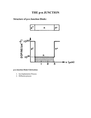
  • 1. THE p-n JUNCTION Structure of p-n Junction Diode: p-n Junction Diode Fabrication: 1. Ion Implantation Process 2. Diffusion process
  • 2. Figure 1 (c)Planar p-n junction diode fabrication on epitaxial substrate by diffusion, (b) Planar p-n junction diode fabrication on epitaxial substrate by ion implantation. Ion Implantation System
  • 3. p-n Junction Diode Physics Space Charge Region: The net positively and negatively charge region shown in Figure 7.2 is called space charge region.
  • 4. Built-in Voltage (Potential) Barrier (Vbi): • Assume that no voltage bias is applied across the p-n junction barrier. • So the p-n junction is in the thermal equilibrium- the Fermi level is constant throughout the system. • The conduction band and valency band energies must bend in the space charge region to accommodate the carriers. • The energy separation between the conduction bands in p- and n-type semiconductor is the built-in voltage Vbi. The built-in voltage can be found from the energy separation of intrinsic Fermi level in p- and n-regions. We can define the potentials ΦFn and ΦFp.
  • 5. Electric Field: An electric field is created in the space charge region by the separation of positive and negative charges. We will assume that the space charge region abruptly ends in the n-region at x = +xn and abruptly ends in the p-region at x = - xp (xp is a positive quantity).
  • 6.
  • 7. E Figure 7.5 is a plot of the electric field in the space charge region. The electric field direction is from the n to the p-region or in the negative x direction for this geometry.
  • 8. Where C1 = constant of integration, The potential is equal zero at x = -xp The constant of integration is found as:
  • 9. Space Charge Width: The space charge region extends into the p- and n- regions from the metallurgical junction. The space charge region can be defined using Equation (7.17) as:
  • 10.
  • 11. Comparative Study of Space Charge for Various Bias Condition F. Biasing R. Biasing Barrier potential Height BPH: Vbi - Vf BPH: Vbi+VR (BPH): Vbi (Vo) Vf = F. Biasing VR = R. Biasing
  • 12. Space Charge Width and Electric Field: Figure 7.8 shows a p-n junction with an applied reverse-bias voltage VR. The electric field in the space charge region and the applied electric field Eapp are induced by the applied electric field. E • At the edge of depletion region (space charge region) at xn and xp, the electric field is almost zero. • Therefore, the electric field at the neutral zone is zero. • The direction of the electric field from n-regions (+ve charge) to p-region (-ve) charge.
  • 13. The total space charge width can be expressed as:
  • 15. JUNCTION CAPACITANCE: Since a separation of positive and negative charges is existing, a capacitance is associated in the p-n junction. The charge densities are changing with variation of R. biasing VR to dVR. The junction capacitance can be expressed as: The space charge width under R. Biasing
  • 16.
  • 17. ONE SIDED ABRUPT JUNCTION: