1. March 2009
Vol. 20 No. 3 | $8.25
www.osa-opn.org
RISK AND RESEARCH: HOW TO MAINTAIN A DIVERSE PORTFOLIO
Optics &
Photonics
News
A New Era
in Optical
Integration
C.V. Raman and
the Raman Effect
Amateur Astronomy
Gets Professional
Optical Fiber
Sensors
2.
3. OPN March 2009 | 1
FEATURES | CONTENTS
[ COVER STORY ]
20 A New Era in Optical Integration
The Internet is increasingly taxing optical networks, and conventional network architecture
cannot provide the scalability required to meet this demand. These authors advise
telecommunications professionals to follow the lead of the microelectronics industry—
by focusing on integrated solutions.
Jacco L. Pleumeekers, Peter W. Evans, Wei Chen, Richard P. Schneider Jr. and
Radha Nagarajan
26 Optical Fiber High-Temperature Sensors
Optical fiber sensors allow researchers and engineers to make accurate, reliable
measurements under high-temperature conditions.
Anbo Wang, Yizheng Zhu and Gary Pickrell
32 The Professional World of Amateur Astronomy
The work of today’s amateur astronomers goes far beyond peering through a telescope on
a lonely mountaintop. Thanks to advances in solid-state imaging, software and inexpensive
optics, they are collecting professional-quality data and making their own discoveries.
Patricia Daukantas
40 C.V. Raman and the Raman Effect
Barry Masters describes the life and legacy of one of the most important optical
scientists of the 20th
century.
Barry R. Masters
New technologies
will be needed
for photonic
integration to scale
to a “photonic
Moore’s Law.”
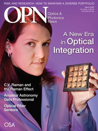
COVER PHOTO: Infinera’s
Sheila Hurtt holds a tray
containing 16 photonic
integrated circuits.
Photo by Gene Lee.
OPN March 2009
Vol. 20, No. 3
Infinera’s Leigh Wade configures a
system at the company’s system lab.
The DTN system can accommodate
four photonic-integrated-circuit-
based line cards, each with data
transmission capacity of 100 Gb/s.
Gene Lee/Infinera
6. 4 | OPN March 2009 www.osa-opn.org
PRESIDENT’S MESSAGE
t several crisis points over the last century, large teams of high-level scientists and
engineers mobilized to spearhead intense efforts to solve critical societal problems. These
efforts not only produced the desired scientific breakthroughs, but also led to significant
investments in basic and applied research and renewed public awareness of the scientific
community’s tremendous capacity for innovation. The current energy crisis calls for just
such a massive, coordinated effort. We are at a unique moment in time, with a new admin-
istration in the United States committed to supporting initiatives focused on overcoming
the energy and environmental crises.
Recently, President Barack Obama, in his speech nominating OSA member Steven Chu
as the new U.S. Secretary of Energy, announced that the pursuit of alternative and renew-
able energy sources would be a “guiding purpose of the Department of Energy as well as a
national mission.” Noting that energy independence lies “in the power of wind and solar
[and]...in the innovation of our scientists and entrepreneurs,” Obama called for a “sus-
tained, all-hands-on-deck effort” to address global energy concerns.
Renewable energy based on solar, wind and biomass offers viable alternatives to fossil
fuels. These options can greatly diminish a nation’s dependence on foreign energy, reduce
greenhouse gas emissions, protect and preserve natural resources and stimulate economic
growth through the development of new industries and technologies.
The OSA community is uniquely positioned to play a prominent role in the further devel-
opment of solar and other renewable energy technologies. We have the knowledge, expertise
and resources to achieve significant advances in both research and applications—but we can
only be successful if we marshal our resources and make the commitment to join in the “all-
hands-on-deck effort” that President Obama and Secretary Chu are organizing.
In June 2008, OSA held a very successful two-day Solar Energy topical meeting at
Stanford University. At this meeting, an international group of leading scientists reported
on new photovoltaic materials in combination with nanostructured electrodes, flat panel
photovoltaic devices incorporating plasmonic resonances and nonimaging concentrators, all
of which have the potential to significantly enhance solar energy efficiency. We are currently
planning a second solar meeting to be held at MIT from June 24-25, 2009. I encourage all
OSA members interested in this area to attend.
In addition, we are forming an officers’ advisory group chaired by OSA President-elect
Jim Wyant to lead our activities as OSA expands its efforts in solar energy. I invite all OSA
members as well as the greater optics and photonics community to volunteer to put your
expertise to work on this vital challenge.
If you’d like join me in this effort, please send a message to osapresident@osa.org. Work-
ing together, we can be a significant force in solving the world’s energy needs.
— Thomas M. Baer
OSA President
We are forming
an officers’
advisory group
chaired by OSA
President-elect
Jim Wyant to lead
our activities as
OSA expands its
efforts in solar
energy. I invite all
OSA members to
put your expertise
to work on this
vital challenge.”
A
“
7. OPN March 2009 | 5
OEM
Biomedical
R&DImaging
Laser
Applications
NEED STOCK
OR CUSTOM
FILTERS?
need a volume or
custom quote?
ContaCt our
sales department today
or to receive your FREE catalog!
more optics
more technology
more service
• More than 1,300 Stock Filters
Available for Same Day Shipping
• Custom Designs & Coatings Available -
Over 25 Years Coating Experience
• High Transmission, Deep Blocking
Fast Delivery
Free Technical Support
800.363.1992 | www.edmundoptics.com/OP
Visit us at
Defense,security,& sensing
Booth 1029
MANAGING EDITOR Christina E. Folz
CREATIVE DIRECTOR Alessia Hawes Kirkland
SENIOR WRITER/EDITOR Patricia Daukantas
GRAPHIC DESIGNER Marko G. Batulan
PRODUCTION MANAGER Stu Griffith
PRODUCTION ASSISTANT Carlos X. Izurieta
PUBLISHER John Childs
ASSOCIATE PUBLISHER Alan N. Tourtlotte
ADVERTISING SALES Anne Jones
202.416.1942
adsales@osa.org
EDITORIAL ADVISORY COMMITTEE CHAIR James Zavislan
University of Rochester
EDITORIAL ADVISORY COMMITTEE Judith Dawes
Macquarie University, Australia
Madeleine Glick
Intel Research
Julio Gutierrez-Vega
Tecnologico de Monterrey, Mexico
Rongguang Liang
Carestream Health
Carlos Lopez-Marsical
National Institute of Standards and Technology
Lynne Molter
Swathmore College
Brian Monacelli
the Optical Sciences Company
Ali Serpenguzel
Koç University, Turkey
Maria Yzuel
University Autonoma de Barcelona, Spain
CONTRIBUTING EDITORS François Busque
Fovea Technologies Inc.
Alexandre Fong
Optronic Laboratories Inc.
G. Groot Gregory
Optical Research Associates
Bob D. Guenther
Duke University
John N. Howard
Air Force Geophysics Laboratory (Retired)
Bob Jopson
Bell Labs, Lucent Technologies
R. John Koshel
Photon Engineering LLC
Brian Monacelli
the Optical Sciences Company
Stephen R. Wilk
Cognex Corp.
OSA Board of Directors
President Thomas M. Baer
President-Elect James C. Wyant
Vice President Christopher Dainty
2008 President Rod C. Alferness
Treasurer Stephen D. Fantone
Executive Director Elizabeth A. Rogan
Chair, Publications Council Govind P. Agrawal
Chair, Board of Editors Tony F. Heinz
Chair, Corporate Associates Paul M. Crosby
Chair, MES Council Irene Georgakoudi
Co-Chairs, Science and Engineering Council David N. Fittinghoff and Edward A. Watson
Chair, International Council Satoshi Kawata
Directors-at-Large Neal S. Bergano, Thomas Elsaesser,
Alexander L. Gaeta, Christoph S. Harder,
Wilhelm G. Kaenders, Lenore McMackin,
Masataka Nakazawa, Bishnu Pal,
Philip St. J. Russell and David F. Welch
Optics &
Photonics
News
THE MAGAZINE OF THE OPTICAL SOCIETY
8. Prices subject to change.
www.cambridge.org/us/physics 1-800-872-7423
New and Forthcoming Titles in Optics
from Cambridge University Press
Forthcoming…
Polarization Holography
Ludmila Nikolova and P. S. Ramanujam
$115.00: Hb: 978-0-521-50975-6: 280 pp.
Forthcoming…
Cambridge Illustrated Handbook of
Optoelectronics and Photonics
Safa Kasap, Harry Ruda, and Yann Boucher
$250.00: Hb: 978-0-521-81596-3: 576 pp.
Forthcoming…
High-Speed Electronics and
Optoelectronics
Devices and Circuits
Sheila Prasad, Hermann Schumacher,
and Anand Gopinath
$90.00: Hb: 978-0-521-86283-7: 496 pp.
New!
Classical Optics
and its Applications
Masud Mansuripur
$90.00: Hb: 978-0-521-88169-2: 720 pp.
Fundamentals of
Photonic Crystal Guiding
Maksim Skorobogatiy and Jianke Yang
$120.00: Hb: 978-0-521-51328-9: 280 pp.
Geometrical and Trigonometric Optics
Eustace L. Dereniak and Teresa D. Dereniak
$80.00: Hb: 978-0-521-88746-5: 424 pp.
Laser Fundamentals
William T. Silfvast
$80.00: Pb: 978-0-521-54105-3: 666 pp.
Introduction to Nanoelectronics
Science, Nanotechnology,
Engineering, and Applications
Vladimir V. Mitin, Viatcheslav A. Kochelap,
and Michael A. Stroscio
$80.00: Hb: 978-0-521-88172-2: 348 pp.
Introduction to the Theory of
Coherence and Polarization of Light
Emil Wolf
$45.00: Hb: 978-0-521-82211-4: 236 pp.
2nd
Edition
2nd
Edition
9. Please direct all correspondence to the Editor,
Optics & Photonics News, The Optical Society,
2010 Massachusetts Ave., N.W., Washington,
D.C. 20036. E-mail: opn@osa.org.
OPN March 2009 | 7
FEEDBACK | LETTERS
Photorealistic
Rendering
I most certainly enjoyed
your article on photore-
alistic rendering (January
2009). It is mind-
boggling to think
of how far we’ve
come, and I was
interested to learn
about the techniques
and technology that
have made it possible.
I do have one small
nit to pick, though. In
the interest of technical
accuracy, I would like to
mention that, although
motion pictures are taken
at 24 frames per second and the film
runs through the projector at the same
rate, each image on the screen is inter-
rupted once during its residence in the
projector gate. Thus, the sentence in
your article that reads “The audience
sees a single frame for only 1/24 of a
second,” might be better expressed as,
“The audience sees a single frame twice
for about 1/96 of a second each time
for a total viewing time of about 1/48
of a second.”
Projectors have a circular shutter—
with two open quadrants and two
opaque quadrants—that rotates once
per frame. One of the opaque quadrants
blocks the light from the screen while
the film is being pulled down to the
next frame. The other opaque quadrant
brings the “flicker” frequency up to 48
per second, which is above the threshold
at which the viewer will see flicker on
the screen at normal screen brightness.
(Note: For silent film projectors, where
the film runs at a nominal 16 frames
per second, the shutter has six segments,
three open and three opaque.)
Here’s another statistic: A two-hour
film will have 172,800 frames.
Woodlief Thomas, Jr.
Merriwood@aol.com
Naples, N.Y., U.S.A.
OSA Historians
I am a longtime fan of your
articles and lectures on the
history of optics, and I partic-
ularly enjoyed your latest article on OSA
historians (January 2009). However,
there is a minor error in your discus-
sion of Hilda Kingslake. Hilda died in
February 2003, some 20 months before
the 75th anniversary of the Institute of
Optics, and she had been incapacitated
for a few years prior to that. Unfortu-
nately, she was thus not able to write the
history of the Institute of Optics for its
75th anniversary. I assumed the task of
editing that volume, which included,
among its 75 essays, 12 from Hilda’s
earlier 50-year history.
Carlos Stroud
stroud@optics.rochester.edu
Rochester, N.Y., U.S.A.
JOHN HOWARD REPLIES: I did indeed
make a dumb mistake in the January
history column. I simply got a bit mixed
up by reading her column on the His-
tory of the Institute just as I was writing
about OSA’s 50th Anniversary. I read
her column two or three months ago
and just didn’t keep good enough notes.
Sorry about that!
John N. Howard
Contributing Editor,
The History of OSA
alistic rendering (January
have made it possible.
I do have one small
nit to pick, though. In
the interest of technical
accuracy, I would like to
mention that, although
motion pictures are taken
history of optics, and I partic-
ularly enjoyed your latest article on OSA
AdvAnces in imAging
REGISTER
TODAY
Digital Holography
and Three-Dimensional
Imaging (DH)
Fourier Transform
Spectroscopy (FTS)
Hyperspectral Imaging
and Sensing of the
Environment (HISE)
Novel Techniques
in Microscopy (NTM)
Optical Trapping
Applications (OTA)
Advances in Imaging includes five
Topical Meetings to bring together
leaders from these technical areas
to network, discuss, and share
information and research. Take this
opportunity to learn more about
your own and other related fields.
Register today for the Advances
in Imaging 2009 OSA Optics &
Photonics Congress!
April 26-30, 2009
Sheraton Vancouver Wall
Centre Hotel
vancouver, bc, canada
hotel reservation deadline:
MArCH 25, 2009
pre-registration deadline:
AprIl 1, 2009
FOr THE lATEST INFOrMATION
ON All MEETINgS VISIT
www.osa.org/congresses
Five ColloCAted topiCAl Meetings
And exhibit
2009 osA optics & photonics Congress
10. 8 | OPN March 2009 www.osa-opn.org
SCATTERINGS | NEWS
that wavelength. The minimum resolu-
tion for normal microscopy is 200 nm.
However, that is problematic for cell
biologists who would like to view struc-
tures smaller than that.
Electron microscopy and X-rays
image smaller objects—but they can
only be used on dead, fixed cells. For live
cells, even ultra-
violet light is too
energetic, ionizing
molecules and
disrupting normal
functioning. “For
biologists look-
ing at live cells,”
Hell says, “optical
microscopy is the
only option.”
All optical
fluorescence meth-
ods depend in one
way or another on
being able to turn
fluorescent mol-
ecules on and off
and build up an
image over time.
STED micros-
copy incorporates
confocal imag-
ing to reduce the
resolution out of
Fluorescent optical microscopy
is allowing researchers to image
features much smaller than the diffrac-
tion limit of visible light. This imaging
technique, called nanoscopy, can yield
resolutions down to hundredths of a
micron—the size of large molecules.
These methods have been in develop-
ment for the past 15 years, since Stefan
Hell, now director at the Max Planck
Institute for Biophysical Chemistry
in Göttingen, Germany, and head of
the department of nano-biophotonics,
reported the stimulated emission deple-
tion microscopy (STED) method (Opt.
Lett. 19, 780). Now Hell is educating
the optics and biotech communities
about nanoscopy.
How does it work? The Abbe limit
claims that objects illuminated with the
light of a certain wavelength cannot be
resolved to distances smaller than half
Nanoscopy
Uncovers the
Secrets of Cells
the imaging plane, then excites the fluo-
rophores in the small volume with a laser
pulse at the absorption wavelength.
Before the sample fluoresces, how-
ever, a second laser pulse, at a longer
wavelength, depletes the energy from
most of the confocal area. This pulse
may be donut-shaped, leaving a small
spot untouched in the center. Fluores-
cence then comes from only the center
area. The smaller that area, the better
the resolution.
In theory, the lower limit to the reso-
lution is a single molecule. The tradeoff,
however, is the reduction in signal (and
the cost of the equipment).
In practice, Hell’s group has demon-
strated resolutions of less than 20 nm
(Opt. Express 16, 4154). STED requires
relatively high laser intensities, but other
methods have different intensity require-
ments, depending on the lifetimes of
their on and off states.
The journal Nature Methods recently
named super-resolution fluorescence
microscopy the 2008 Method of the
Year (Nature Methods 6, 1), and many
research groups are using methods such
as this to image structures and pro-
cesses inside living cells.“Molecular-level
resolution with visible light is, of course,
possible,” says Hell.
— Yvonne Carts-Powell
As the dendritic structures of neurons twist, the tips (indicated by arrows) turn cup-shaped.
Images were obtained with stimulated emission depletion microscopy.
(a) Nanoscale image of the endoplasmic reticulum of living mam-
malian cells labeled with a fluorescent protein. (b) The 2D anisot-
ropy histogram reveals only mobile fluorescent proteins. (c) Image
of b-actin in living cells. (d) This histogram reveals static and free
rotating molecules. (f) Images of immobile (green) and mobile (red)
b-actin are created based on their position in the histogram.
MaxPlanckInstituteofNeurobiology
Opt.Express16,21093(2008)
1 µm
1 mm
1 mm
1 mm
(a)
(b)
(d)
(f)
(c)
(e)
11. OPN March 2009 | 9
Researchers at the Fraunhofer
Institute for Laser Technology
ILT (Aachen, Germany) have devel-
oped a powerful soft X-ray light
source and collector lens system
smaller than 2 m3. The small size
allows it to be integrated directly
into a microscope. The hollow-cath-
ode-triggered pinch plasma—gen-
erated from ionized nitrogen—emits
at 2.88 nm. A prototype microscope
captures 3D images of several-
micrometer-thick samples in tens
of seconds. Klaus
Bergmann, who
leads the team,
adds, “We
will be able
to bring the
exposure
time down
to below
10 s for
the larger
samples too,
by optimizing
the design of the
condenser mirror.”
Anew lasing mechanism was recently
reported from a quantum cascade
laser that appears to depend on non-
equilibrium electrons with high momen-
ta. Kale Franz and others at Princeton
University (N.J., U.S.A.) noticed a
second lasing wavelength, with notably
different characteristics from the design
wavelength (Nature Photon. 3, 50).
Franz and others in Claire Gmachl’s
Mid-Infrared Technologies for Health
and the Environment Center at Princeton
designed and built a laser composed of
interleaved AlInAs barriers and InGaAs
quantum-well layers. But when they test-
ed the quantum cascade laser designed
to emit at 9.5-µm light, they discovered a
second lasing peak at 8.2 µm.
“With population inversion, you’d
normally think of having a pool of
electrons in that upper laser state so
that they can contribute to lasing,” said
Franz. “But we’ve shown that we can
achieve a population inversion—and
lasing—even at a point where we don’t
have that electron pool.”
The second wavelength is generated
by the transition from a different energy
level but still acts as a quantum cascade
laser. It had bizarre characteristics: The
power output increased with rising tem-
perature (over a certain range of tempera-
tures); it competed for electrons with the
primary wavelength; and it had
a lower threshold current than
the primary wavelength.
Mid-infrared lasers that
offer higher efficiency and
work at higher temperatures
could be tremendously use-
ful. One driver for the devel-
opment of quantum cascade
lasers is that they operate in
the mid- and far-infrared range
(roughly 3 to 300 µm in wave-
length), which can be used to detect
traces of water vapor, ammonia, nitro-
gen oxides and other gases that absorb
infrared light. Applications include air
quality monitoring, medical diagnostics,
homeland security, free-space commu-
nications and defense countermeasures.
The new discovery should help make
these devices smaller, more efficient and
more sensitive, Gmachl said.
To explain the phenomenon, the
researchers had to move away from the
standard assumption that the wave-
vector of electrons in both the low and
excited states was zero. In most semi-
conductor lasers, including quantum
cascade lasers, stimulated emission
occurs only from electrons with nearly
zero momentum.
One effect of using a “high k-space”
transition for lasing is that the shape
Lasing Mechanism Depends
on Electron Momentum
DID YOU KNOW?
Princeton graduate students
Kale Franz (left) and Stefan
Menzel have uncovered a
new lasing mechanism in
quantum cascade lasers.
Frank Wojciechowski
Yvonne Carts-Powell (yvonne@nasw.org) is a freelance science writer who specializes in optics and photonics.
Inset: A diatom imaged with a
prototype X-ray microscope.
Fraunhofer Institute for Laser Technology ILT
of seconds. Klaus
Bergmann, who
leads the team,
adds, “We
will be able
samples too,
by optimizing
the design of the
condenser mirror.”
primary wavelength; and it had
the mid- and far-infrared range
length), which can be used to detect
2 µm
of the energy sub-bands changes from
their parabolic shape at k=0. This leads
to suppression of optical absorption by
90 percent, says Franz. Because of the
physical properties of this new energy
space, Franz says, “our laser emission
wavelength and re-absorption wave-
length are different. This means less loss,
lower thresholds, more power, higher
efficiencies...all the things that make
lasers better.”
The researchers are figuring out how
to optimize the new lasing process. The
mechanism may also be applicable to
other types of semiconductor lasers.
12. 10 | OPN March 2009 www.osa-opn.org
OPTICS | INNOVATIONS
CREOL’s
Tech-Transfer
Success Stories
Jenna Reiser and
James Pearson
Savvy industrial leaders know that
they need to build strong partner-
ships with research institutions in order
to capture the best products and talent.
But the transfer of technology from lab
bench to business plan isn’t always as
straightforward as it might seem. That is
why the Center for Research in Optics
and Lasers (CREOL) at the University of
Central Florida (UCF) in Orlando, Fla.,
U.S.A., has dedicated itself to not only
nurturing scientific discoveries in optics,
but to promoting the growth and com-
mercialization of the applications that
result from them.
When executives or entrepreneurs
from a photonics company need tech-
nology for a new product, they often
seek help from university research-
ers who are skilled in both basic and
applied research. UCF fosters these
collaborations through its Photonics
Incubation Program, which is housed in
the CREOL building on UCF’s main
campus and is part of the UCF Technol-
ogy Incubator (UCFTI) within the UCF
Business Incubation program.
The UCF Business Incubation Pro-
gram began in 1999 and, in total, it has
helped more than 90 clients to generate
more than 900 new jobs and over $200
million in annual revenue. The program
to be one of the largest photonic crystal
growers in the world.
Another successful spin-off, Optium,
was created in 2000 by CREOL Profes-
sors Guifang Li and Patrick LiKamWa,
along with Paul Yu at the University
of California, San Diego. In 2006,
Optium went public, and, in 2008,
it was acquired by and merged with
Finisar, a global technology leader of
fiber optic subsystems and network
test systems. The combined company is
one of the biggest suppliers of optical
components, modules and subsystems
for the communications industry in the
world, with more than $660 million in
annual revenues.
Leon Glebov, CREOL senior research
scientist, helped found OptiGrate in
2007 using his photo-thermal refractive
glass technology. OptiGrate produces
unique holographic volume Bragg
gratings for optical beam control in
high-power laser systems for myriad
applications, including military laser
devices, optical telecommunication
systems, entertainment systems and
medical and security sensing devices.
A recent CREOL spin-off is BD
Displays, which was founded by Profes-
sors Michael Bass and Dennis Deppe.
The two founders had each conducted
Jacquephoto.com
works with start-up and early-stage com-
panies to provide mentoring and training
in business development, networking
opportunities, access to UCF faculty and
labs, and other tools that are needed to
create financially stable, high-growth,
technology-driven enterprises.
CREOL and the UCFTI have spun
off many photonics-based companies, all
of which continue to spark new areas of
growth. For example, one of the earliest
CREOL spinoff companies is Crystal
Photonics Inc. (CPI), a manufacturer
of optical crystals for many applications
in biophotonics, microelectronics and
photonics. Founded in 1995 by CREOL
Professor Bruce Chai, CPI is now a
multi-million-dollar enterprise located in
Sanford, Fla. The company is positioned
CREOL made significant
contributions to the
intellectual capital of
photonics research. In
fact, in 2008, it helped
propel UCF to a national
patent ranking.
The Center for Research in Optics and Lasers (CREOL) at the University of
Central Florida prides itself on its strong focus on technology transfer—and it
has the multi-million-dollar success stories to show for it.
CREOL Professor Peter Delfyett
(center) helped start Raydiance,
a photonics company based on
CREOL-developed ultrashort-
pulse laser technology.
13. OPN March 2009 | 11
independent research, which, when
combined, provided the foundation for
next-generation high-resolution and high-
brightness micro-displays for various
applications, including training, personal
entertainment and gaming devices.
CREOL Professor Martin Richardson
(who also leads CREOL’s new Townes
Laser Institute) helped form LP Photon-
ics in 2008 to hasten the commercializa-
tion of extreme ultraviolet (EUV) optical
source technology. This new venture will
provide the powerful, reliable, EUV light
source that is needed by the semiconduc-
tor manufacturing industry for the next
generation of optical lithography that
will allow for continued advancement of
Moore’s law.
Barry Schuler, a former CEO and
chairman of AOL, started Raydiance Inc.
in 2004 using ultrashort-pulse laser tech-
nology developed primarily by CREOL
Professor Peter Delfyett. The company
has since raised more than $25 million
of venture capital. Enabled by CREOL
photonics patents, and by software and
rugged fiber optic technology, Raydiance
products provide a versatile, compact,
plug-and-play platform to enable innova-
tion and commercial applications.
CREOL has also made significant
contributions to the intellectual capital
of photonics research. In fact, in 2008, it
helped propel UCF to a national patent
ranking. UCF joined other prestigious
research universities, including the
Massachusetts Institute of Technology
and Stanford University, in the top 10
of the “2008 Patent Scorecard for U.S.
Universities.” UCF also ranked third
in the industry impact category, which
measures the role that university patents
play in serving as a foundation for other
patents and technologies. The rankings
were published in the September 2008
issue of Intellectual Property Today.
One of the ways that UCF cultivates
its intellectual property is through its
Office of Technology Transfer (OTT),
which is part of the UCF Office of
Research and Commercialization
(UCFORC). The OTT has licensing
associates who work with UCF research-
ers to help them protect, manage and
license their intellectual property.
CREOL also has an industrial affiliates
program with more than 60 member
companies. These partners benefit from
CREOL’s strong alliance with other
UCF research units, including the
Nanoscience Technology Center, the
Burnett School of Biomedical Sciences,
the Advanced Materials Processing and
Analysis Center, the Institute for Simula-
tion and Training, the Florida Solar
Energy Center, and UCF’s new College
of Medicine.
Joe Giampapa, the director of
technology transfer in the UCFORC,
speaks highly about CREOL’s talent for
commercializing its research. “CREOL’s
optics research generates a large number
of breakthrough inventions, which pave
the way for greater licensing and spin-out
opportunities,” he said.
CREOL has a long tradition of engag-
ing in technology transfer, beginning with
the vision of its founder Bill Schwartz,
a laser pioneer who proposed creating a
university-based center that would give
Florida’s high-tech industries access to
leading research and facilities in optical
and laser sciences and engineering.
Today, under the leadership of its new
dean, Bahaa Saleh, CREOL is continu-
ing its emphasis on strong research and
partnerships. CREOL hosts two new
research centers funded by the state of
Florida’s Center of Excellence program:
The Florida Photonics Center of Excel-
lence (FPCE), which was started in 2003
with a $10 million Florida grant, and the
Townes Laser Institute, which opened its
doors in 2007 after having been estab-
lished with a $4.5-million grant from the
state, plus matching funds and funding
for UCF faculty.
“Preparing students to function well
in the technological world is essential,”
said Saleh, “and maintaining our strong
links with industry and forging new
links will continue to be of paramount
importance.” t
James Pearson (jpearson@creol.ucf.edu) is
the director of research and administration at
CREOL, The College of Optics & Photonics, in
Orlando, Fla. Jenna Reiser is a communications
consultant for CREOL.
OPTICAL
ISOLATORS
Free Space Isolators
• Epoxy-Free Optical Path
• All Isolators are Set for a Horizontal
Input Polarization
• Units are Available Without Polarizers
to Function as Faraday Rotators
• Custom Wavelengths, Polarizers, and
Apertures Available
Fiber Isolators
• High-Power, Polarization-Independent
or Polarization Dependent Models
• SM or PM Fibers Used on the Input
and Output
• Wavelength Ranges from 780 to 1550 nm
New TOOLS OF THE TRADE Catalog!
Request Online at www.thorlabs.com
30 W to 50 W
SHIPPING FROM
STOCK
OFR_Isolators_2.qxd 12/4/08 4:19 PM Pa
14. www.osa-opn.org12 | OPN March 2009
LIGHT | TOUCH
The Yellow
Sun Paradox
Stephen R. Wilk
Though I am old with wandering
Through hollow lands and hilly lands,
I will find out where she has gone,
And kiss her lips and take her hands;
And walk among long dappled grass,
And pluck till time and times are done
The silver apples of the moon,
The golden apples of the sun.
— The last verse of
The Song of Wandering Aengus by
William Butler Yeats (1865-1939)
If you ask preschool children to draw
the sun, they’ll make a yellow circle,
often with visible rays emanating from
it (and maybe a smiling face). The “gold
ball” in the story The Princess and the
Frog represents the Sun, says mytholo-
gist Joseph Campbell, because gold
is the solar metal. Egyptian, Celtic,
Chinese and Aztec representations of the
sun are made of gold as well. And if you
ask an average person on the street what
color the sun is, he or she would say it
was yellow.
And yet the sun is not yellow. In fact,
sunlight is the very definition of white
light. If the sun were truly yellow, the
colors of everything we see would be
we perceive. But, as Plait points out,
if white objects appeared yellow in the
sky, then clouds would seem yellow, and
they’re not.
A third possibility is that yellow is the
most accurate representation of the sun’s
color when it is low in the sky—the only
time we can look at it without hurting
our eyes. When the sun is high, it’s too
bright to look at. As it approaches the
horizon, more of its light gets scattered
away by the atmosphere, so you can
glance at it more easily. The sun’s color
changes because of that scattering: It
goes from yellowish to orange to red and
finally magenta. Plait finds this claim
interesting but he has some doubts. He
remembers the sun most when it is glow-
ing magenta on the horizon, yet on the
whole he does not perceive it as red.
To get to the bottom of this, I mod-
eled the passage of light from the sun
through an atmosphere that scattered
according to a strict Rayleigh scatter
1/l4
law. I assumed Illuminant D65
(noon daylight), a scattering cross-section
that depends upon the inverse fourth
power of the wavelength (and a loss expo-
nential in the product of this cross-section
times the optical path length, multiplied
subtly altered. As anyone who works in
a lithographic facility knows, working
under truly yellow light can be unnerv-
ing. The CIE coordinates of the standard
illuminants all lie close to (0.3, 0.3), the
white locus of the color diagram.
So the sun is undoubtedly white, yet
everyone seems to perceive it as yellow.
What gives? Phil Plait, who manages
the Web site “The Bad Astronomer”
(on which he exposes examples of bad
astronomy), has put forth some possible
explanations for why people perceive the
sun as yellow.
One is that the same Rayleigh scatter-
ing that is responsible for the sky’s blue-
ness also makes the sun appear yellow,
since some of the blue has been scattered
out. (This is the most common sugges-
tion I hear when I mention the paradox
to people.) But the amount of blue light
scattered out is far too small to have a
noticeable effect on the sun’s color. The
CIE standard illuminants already have
the effects of scattering built into them,
and they predict a white sun.
A second suggestion is that the sun
seems yellow because we are comparing
it to a blue sky. Perception studies show
that the background can affect the color
There are a few things you
can count on in this world:
The sky is blue; grass
is green; and the sun is
yellow…right?
Nicolas Raymond
15. OPN March 2009 | 13
by a constant), and the usual three stan-
dard color functions. I then calculated the
CIE chromaticity coordinates (x,y) in the
usual fashion by numerical integration of
the product of the illuminant, scattering
function and color
over wavelength
space, then normal-
izing the chroma-
ticity coordinates
X, Y and Z.
The results were
interesting. The
starting point, with
negligible scatter,
was the Illuminant
D65 “white point”
of (0.313, 0.329).
However, as soon
as the path lengthened, the trajectory of
the locus of the apparent sun color started
moving directly toward the spectral locus
at about 570 nm, which is about as yel-
low as you can get. It continued toward
this point for some time before veering off
slowly toward 580 nm, which is still well
within what is generally termed “yellow.”
Then it gradually turned orange and then
red, and asymptotically approached the
deep red terminus of the spectral locus.
Its trajectory superficially resembles
the Planckian locus, representing the
perceived color of a blackbody radiator
as it cools—but the differences are sig-
nificant. The blackbody starts not at the
white center, but at the limiting point of
(0.328, 0.502), at the light-blue color of
blue heat. It then arcs across, skirting the
edge of the white region at about 6,000
K before cutting across the yellow range,
between about 4,000 K and 2,500 K, and
asymptotically approaching the red end
of the spectral locus. The difference is that
the Planckian locus curve starts in the
blue and spends much less of its length in
the yellow portion of the color diagram.
So, until the sun gets very low in the
sky and starts to change from orange
to red, it spends all of its time as either
white or yellow. As soon as it is attenu-
ated enough to look at even fleetingly, it
appears yellow, and it remains this way
until it rapidly begins to change color
at sunset.
It’s not just coincidental that the sun
appears mostly yellow—this color is the
complement of the blue sky. On the
chromaticity diagram, it is diametrically
opposite the blue sky locus, which this
calculation sets at
(0.2279, 0.2312)
in the limit of small
amounts of scatter.
The chromatic-
ity coordinates of the
blue sky change very
slowly with increased
scatter distance, ulti-
mately moving toward
the white locus as
the scattering length
approaches infinity.
When you subtract
this blue from the white, you get yellow
as a residue. So, in essence, each of the
possible explanations put forth by Plait
are, in a sense, correct.
Another possible reason for why we
view the sun as yellow could arise from
our ancestors. Early humans would
naturally view the sun as a “fire in the
sky,” since they were accustomed to using
fire to warm themselves and prepare
food. They would believe the sun to be
yellow-orange—the most prominent
color in flames consisting of soot heated
by combustion. And their experience
would confirm this belief; they would see
a yellow sun in the sky—as soon as it was
dim enough to be viewed directly. t
Stephen R. Wilk (swilk@comcast.net) is an optical
engineer based in Saugus, Mass., U.S.A.
References and Resources
>> F. Birren. The Story of Color: from Ancient
Mysticism to Modern Science, Crimson
Press, Westport, Conn., U.S.A. (1941).
>> M.N. Perrin. “Calibrating the Color Tem-
perature Relation: The B-V Color of the
Sun,” Annales de Physique 6 (1-2), 115-20
(1981).
>> P.C. Plait. Misconceptions and Misuses
Revealed, from Astrology to the Moon
Landing “Hoax,” Wiley and Sons. (2002).
Also see his Web site at http://blogs.
discovermagazine.com/badastronomy/.
>> The Munsell Color Laboratory Resources
Page: www.cis.rit.edu/mcsl/online/cie.
php.
As soon as the sun is
attenuated enough to
look at even fleetingly,
it appears yellow, and
it remains this way
until it rapidly begins to
change color at sunset.
OPTOMECHANICS
New TOOLS OF THE TRADE Catalog!
Request Online at www.thorlabs.com
NEW
PRODUCT
IDEAS WELCOME
www.thorlabs.com
Hungry for your
thoughts…
Bringing Automated
Control to the Table
NEW
Gimbal Mount
• Over 1,200 Products
• Shipping From Stock
• Mounting Essentials
• Cage Systems
• High-Precision Positioning
• OEM Designs and Production
Mech_OPN_rev3.qxd 11/3/08 5:07 PM Page
16. 14 | OPN March 2009 www.osa-opn.org
OPTICS | CONVERSATIONS
OPN Talks with …
Philippe Morin
President of Metro
Ethernet Networks at
Nortel and OFC/NFOEC
Keynote Speaker
and high-performance digital signal
processing techniques that result in
easily deployable 40 G/100 G transmis-
sion systems. The solution integrates
dispersion compensation technology
into the world’s first coherent 40 Gbps
receiver, for both chromatic and polar-
ization mode dispersion. This is a novel
way of solving high-speed networking
for our customers—and frankly, this
is the only technique being discussed
by standards organizations as a practi-
cal option for 100 G transmission in
50 GHz systems. The solution is being
deployed in metropolitan, long-haul
and submarine applications that operate
over a variety of line systems, including
foreign line systems.
How does Nortel stay at the fore-
front of emerging technology?
It is part of our DNA. We invest and
participate in all the relevant standards
bodies to ensure that we continue to
distinguish ourselves. We recently
launched our WDM PON Ethernet
access solution in the fourth quarter; it
For the past 20 years,
Philippe Morin has
watched the field of
optical communications
grow into a multi-billion-
dollar industry that offers
cutting-edge solutions
to meet the demands of
today’s super-fast, high-
bandwidth networks.
Morin is the president of
Metro Ethernet Networks
for the Canadian
telecommunications
equipment-maker Nortel.
He leads the company’s
production and logistics,
research and product
development, as well
as business operations
for Nortel’s optical
and carrier Ethernet
portfolios.
What are the latest trends in Metro
Ethernet? What is needed to make
100 GbE a deployable reality?
In recent years, the Metro Ethernet busi-
ness has been focused on consolidating
Ethernet and optical capabilities, where
Carrier Ethernet and WDM technologies
are being recognized as the most efficient
and cost-effective means of transporting
today’s traffic across the network. We
expect to see a lot of innovation behind
these technologies as we move forward.
The 100 GbE (that’s 100 Gigabits per
second of Ethernet traffic on a single
port) will provide a means for operators
to both scale and simplify their networks.
The technology will be deployed when
the 100 GbE standards are finalized and
volume-deployable 100 G optical solu-
tions become available.
Tell us about the 40 G/100 G
Adaptive Optical Engine, one of
Nortel’s most recent innovations.
In our 40 G/100 G Adaptive Optical
Engine, we use advanced modulation
17. OPN March 2009 | 15
provides a dedicated wavelength of high-
capacity bandwidth per user. E-SPRING
is an imminent technology that we are
developing by transposing some of the
traditional carrier grade SONET/SDH
shared ring values to Ethernet.
What changes has Nortel seen
over the past 20 years? Where is
it headed?
After having survived both the boom
and bust cycles of this business, I can
say that the overall pace of the industry
has increased dramatically over the last
15 years; companies need to move faster
to stay abreast of each
other in this crowded
market. At Nortel,
the combining of our
Carrier Ethernet and
optical businesses has
allowed us to extend
our innovation capa-
bilities with Ethernet
solutions and maintain
our leadership posi-
tion as one of the few
global optical vendors
with solutions in each
market segment.
What does the future of optical
technology in telecommunications
look like?
The increased connectivity of high-
bandwidth applications between a
larger number of users signifies that
optical systems will need to scale in a
simple fashion and be very flexible so
that a wavelength can easily be routed
anywhere in the network. As digital
signal processing techniques become
the increasingly popular choice for
correcting signal degradations, clumsy
custom-engineered optical compensation
devices such as dispersion compensation
modules or PMD compensators will
become obsolete.
How did you get involved in optical
communications?
I have worked in the optical business for
the past 20 years in various positions,
including product management, sales
and marketing. With my engineer-
ing background, I have found it very
interesting to remain close to a technol-
ogy that we knew from early on would
revolutionize the speed of global business
operations and increase the power of
personal networking.
What has been the most significant
advance in telecom that you’ve
witnessed? What’s been the most
surprising trend?
The biggest advance in the optical
industry is the incorporation of wireless
transmission techniques,
in particular coherent
detection, after 20 years
of systems that used
intensity modulation
detection. The new tech-
niques enable deployable
high-capacity transmis-
sion systems.
With respect to a
surprising trend, I don’t
think anyone realized
the speed at which net-
work bandwidth would
be depleted, with video
being the key gobbler in a variety of
applications, including peer-to-peer net-
working, personal video recorders, home
theater TV systems, and even gaming
systems such as the Xbox LIVE.
Can you give us a sneak preview
of what you will discuss in your
plenary presentation?
I will present my vision of where the
optical network industry is headed. I
will also speak to the innovations that I
believe are necessary as we move forward
in this difficult economic environment.
Philippe Morin will deliver his plenary talk
on Tuesday, March 24, 2009, at the OFC/
NFOEC conference in San Diego, Calif.,
U.S.A. For more information or to register,
visit www.ofcnfoec.org.
Angela Stark (astark@osa.org) is OSA’s public
and government relations specialist.
The biggest
advance in the
optical industry is
the incorporation of
wireless transmis-
sion techniques, in
particular coherent
detection.”
“
NEW!
• Dual-Channel Power and Energy Meters
• Analog and Digital Displays
• High-Power and
High-Sensitivity Models
- Si and Ge Sensors
- Thermal Sensors
- Energy Sensors
- Integrating Spheres
• Interchangeable Sensor Heads
• NIST-Traceable Calibration
OPTICAL
POWER METERS
NEW
PRODUCT
IDEAS WELCOME
www.thorlabs.com
Hungry for your
thoughts…
New TOOLS OF THE TRADE Catalog!
Request Online at www.thorlabs.com
PM100D
NEW!
2_PowerMeters_LFW_07.qxd 10/3/08 5:23 P
18. 16 | OPN March 2009 www.osa-opn.org
Risk and Research:
Maintaining a
Diverse Portfolio
Ken Baldwin
How can funding agencies strike the
right balance between financing “high-
risk, high-reward” research—work that is
initially uncertain but that could translate
into major breakthroughs—and more
modest studies that will likely produce
solid, incremental results?
c Capacity risk: The chance that
research funding, staff or equipment
may not be sufficient to perform the
required task. (As we all know, some-
times the true cost of research turns
out to be far different from that in
initial proposals.)
c Failure risk: The risk that research
might fail to meet a particular
objective. There are rarely complete
failures, however, since research can
always point to avenues for further
work.
c Collaborative risk: The possibility
that research is constrained by “safe”
choices of collaborators, such as
those from lead institutions or with
strong reputations. This is a very real
issue in multi-disciplinary research.
c Precedence risk: The chance that
funded research will become obsolete
because another investigator or group
makes the finding first.
c Regulatory risk: The risk (particu-
larly to institutions) that research
transgresses certain ethical, regula-
tory and commercial constraints.
The FASTS forum focused primar-
ily on transformative risk as the key
VIEWPOINT
The global financial crisis has
brought the concept of risk to the
forefront of our collective consciousness.
It has also put pressure on the public
and private entities that fund scientific
research, given the competing needs of
other sectors of the world’s economy.
Yet now is arguably the time to
invest in research that can help us
secure a better future. It is also an
ideal opportunity to reflect on how we
can create a robust and flexible fund-
ing system. In Australia this year, the
Federation of Australian Scientific and
Technological Societies (FASTS) held a
forum on Risk Aware Research, which
focused especially on the challenges
faced by small nations. It explored how
risk should be addressed across a limited
range of research funding programs.
Risk in research has many defini-
tions. We therefore developed, per-
haps for the first time, a “taxonomy
of risk” to provide a starting point for
discussion:
c Transformative risk: The risk
that funding for ideas that could
transform the way we think may
be delayed or denied because the
research violates existing interests or
views.
VIEWPOINT
challenge to research funding programs.
The U.S. National Science Foundation
(NSF) has also recently studied transfor-
mative research. According to the NSF,
transformative research is “characterized
by its challenge to current understand-
ing or its pathway to new frontiers.”
The NSF report recognized the
importance of fostering transformative
risk. Its key recommendation was “that
the NSF develop a distinct, foundation-
wide transformative research initiative
distinguishable by its potential impact
on prevailing paradigms and by the
potential to create new fields of science,
to develop new technologies and to
open new frontiers.”
However, the report recognized
that the peer-review process is often
risk-averse. It notes that transformative
research does not “fare well wherever a
review system is dominated by experts
highly invested in current paradigms
or during times of especially limited
budgets.”
There are ways that researchers can
counter the conservatism of the peer-
review process, however. For example,
they can game the system by putting
forward “safe” proposals based on
incremental work for which they have
already achieved results. Then, after
19. OPN March 2009 | 17
peer reviewers recom-
mend funding, the
investigators can go on
to pursue more specula-
tive research, since
they already have the
incremental results “in
the bag.”
Such gaming gives
researchers built-in agil-
ity. However, allowing
perverse behavior to
counter inherent short-
comings is bad policy.
It is better to establish
the right incentives in the first place.
So how can transformative risk be
encouraged? The FASTS forum identi-
fied the following approaches to embed
risk-awareness in funding programs:
c Aggregation: The sheer size of
research programs can provide the
flexibility needed to encourage
transformative risk. Centers of excel-
lence and other large programs allow
the quarantining of discretionary
funds for more risky projects. Yet it is
important to recognize that risk can-
not easily be borne at the individual
project level, particularly in tight
funding environments.
c Diversity: A portfolio approach that
provides a large choice of funding
bodies and programs can create a
range of risk-friendly mechanisms to
encourage transformative research.
c Time: Agility is also encouraged
through longer timeframes for re-
search programs, particularly when
coupled with aggregation.
c Flexibility: Programs need to ensure
that the funding rules allow research
to change direction if necessary. This
is sometimes achieved by not requir-
ing a project to report against the
original objectives, thereby encour-
aging researchers to move in new
directions.
c Rewards: Contracts should encour-
age the handing back of funds in
cases where research reaches a dead
Funding programs
that encourage
risk are as much
about developing
the human
capacity to push
the boundaries
of knowledge as
they are about the
research outputs
themselves.
end. This should be
treated as good profes-
sional practice, where
favorable consideration
is given to provid-
ing additional funds
for future successful
applications by the same
investigators.
c Costs: By minimiz-
ing the regulatory
and transaction costs
of grant applications,
researchers will be
encouraged to apply more often for
grants that might be more risky.
c Context: A flexible risk-evaluation
framework will encourage risk in the
appropriate context. For example, the
evaluation of research in a commer-
cial setting must be different than
that for fundamental research at
universities.
DARPA (the Defense Advanced
Research Projects Agency) in the United
States funds high-risk research aimed at
identifying potentially disruptive threats
and challenges. The NSF SGER (Small
Grants for Exploratory Research) fund
is also aimed at testing new, high-risk
ideas; this option is particularly useful
for early-career researchers.
Funding programs that encourage
risk are as much about developing the
human capacity to push the boundar-
ies of knowledge as they are about the
research outputs themselves. Encour-
aging risk-aware research can help
scientists and engineers to investigate
bold new ideas and free us all to create
an exciting future. t
Ken Baldwin (Kenneth.Baldwin@anu.edu.au) is
a professor of physics at the Australian National
University and president of FASTS. He is a cur-
rent member of the Public Policy Committee.
[ References and Resources ]
>> The Federation of Australian Scientific and
Technological Societies: www.fasts.org.
>> “Enhancing Support of Transformative
Research at the National Science
Foundation,” NSF document NSB-07-32,
May 7, 2007.
Revolutionizing
data shaRing in
publishing
n Interact with large
2D and 3D images
and datasets associated
with peer-reviewed
journal articles.
n Explore image data
quickly and easily over
the internet.
Free access to
Interactive Science
Publishing articles
now in Optics Express
and Journal of the
Optical Society of
America A.
ISPInteractive Science Publishing
OSA
Introduces
Learn more at
www.opticsinfobase.org/isp
Interactive
Science
Publishing
(ISP)
20. www.osa-opn.org18 | OPN March 2009
OSA | HISTORY
George Ellery Hale served as the
Society’s first vice president from
1916 to 1917, during the presidency of
Perley Nutting. He was a charter member
and he became an Ives Medalist in 1935.
(Hale never became president; it wasn’t
until 1922 that OSA leadership decided
that VPs would automatically advance to
that post at the next election.)
Hale was interested in solar astronomy,
and, in 1888, while still an undergraduate
at MIT, he invented the spectrohelio-
graph, with which he discovered solar vor-
tices and the magnetic fields of sunspots.
After MIT, he returned to his father’s
house in Kenwood, Ill.—a district in
south Chicago not far from the universi-
ty—where he continued his studies from
his own private observatory using a 12-in.
refractor telescope. His efforts caught the
eye of William Rainey Harper, president
of the University of Chicago, who wrote
on July 1, 1892, to ask if Hale would be
interested in joining the university.
The 24-year-old Hale asked his father
for advice—and got a lot more than that
in return. The elder Hale wrote to Harper
that same day, offering to donate the
Kenwood Observatory and its 12-in. tele-
scope to the University of Chicago if the
university would: 1) appoint his son as an
associate professor of astrophysics; 2) raise
$250,000 over the next three years for an
even larger observatory; and 3) appoint
George as director of the observatory.
Harper took that response to the next
board of trustees meeting, and George’s
appointment (although with no salary)
was approved on July 26, 1892.
Hale was pleased with his new academ-
ic status, and he took off in early August
of aperture and a gain of 23 percent in
light-gathering ability. The new telescope
would then be the world’s largest, prob-
ably for many years! (It is still the world’s
largest refractor.) Hale said the mounting
and tube could be finished in time to be
displayed at the Columbian Exposition
in Chicago in May 1893. Yerkes’ name
would be remembered for all time!
All of this went to Yerkes’ head, and
he agreed to support the project. He said:
“I don’t care what the cost; just send me
the bill!” The Chicago papers headlined
that Yerkes will spend a million dollars to
“Lick the Lick.”
Within a week, a contract was
awarded to Clark & Sons to finish the
disks. Another contract went to War-
ner & Swasey of Cleveland to build the
mounting and 40-in. telescope tube.
Donors came forward offering land to
site the observatory; altogether, 27 sites
were proposed. Hale and Harper decided
that the site should be within 100 miles
of the university. Hale wrote to nine well-
known astronomers for advice about the
effects of smoke, electric lights, vibrations
from passing trains and bad weather.
They finally chose Williams Bay,
on Lake Geneva, Wis.—76 miles from
Chicago. In December 1892, Yerkes hired
Henry Ives Cobb, the architect of the
University, to design the Observatory.
(Construction began in 1895, and the
telescope’s first observations were made in
1897.) All in all, it was a busy six months
for the young Hale! t
John N. Howard (johnnelsonhoward@gmail.com)
is the founding editor of Applied Optics and
retired chief scientist of the Air Force Geophysics
Laboratory.
for a vacation in upstate New York, while
he prepared a paper for an AAAS meet-
ing in Rochester in September. After his
talk, he was relaxing one evening in the
lobby of the Powers Hotel, talking with
Edwin Frost, the Dartmouth astronomer.
Nearby, Alvan C. Clark, the well-known
optician from Cambridgeport, Mass., was
telling a story about two large disks of
optical glass, 42-in. in diameter, that had
been cast by Mantois of Paris in 1889 for
the University of Southern California.
USC had been planning an observato-
ry on Mt. Wilson, and Clark was asked to
figure the disks. To finance the telescope,
one of the USC trustees had pledged a
large tract of land; but a real estate bubble
had burst, and that land was now almost
worthless. USC had defaulted on its pay-
ments and owed Clark $16,000 for work
he had already done.
Hale cut short his vacation and hurried
back to the university to talk to Harper
about financing Clark’s work to build
a large telescope. (By coincidence, big
telescopes were in the news: On Septem-
ber 9, the newspapers carried a story that
the astronomer Edward Barnard had just
discovered a fifth satellite of Jupiter—one
more than the four seen by Galileo. Bar-
nard made this discovery using the world’s
largest telescope, the 36-in. refractor at
Lick Observatory.)
Harper sent a note to Charles Tyson
Yerkes, the financier who had built the
Chicago electric railway system, and, on
October 4, Harper and Hale met with
Yerkes in his office. Hale told Yerkes
that, using Clark’s optical disks, they
could build a telescope even larger than
the one at Lick—with four more inches
George Ellery Hale and
the Yerkes Observatory
John N. Howard
How OSA’s first vice president “licked the Lick.”
George E. Hale observing
with the spectrograph of
the Snow telescope.
The Hale Observatories, courtesy AIP Emilio Segre Visual Archives
21. san jose, california, Usa
Technical conference:
october 11-15, 2009
exhibiT:
october 13-14, 2009
Visit
www.frontiersinoptics.org
for information and to submit papers.
call for PaPers
SubmiSSion DeaDline:
Tuesday, May 26, 2009
12:00 p.m. noon eDT (16.00 GMT)
2009 PhAST/Laser Focus World
Innovation Awards
Award Sponsors:
®
Announcing
CALL FOR ENTRIES
Submission Deadline:
March 27, 2009
Submission information and entry form:
www.phastconference.org/innovation
PhAST is
collocated with
ConferenCe
May 31–June 5, 2009
Baltimore Convention Center
Baltimore, Maryland, USA
exhibition
June 2–4, 2009
Baltimore Convention Center
Baltimore, Maryland, USA
PhAST and Laser Focus World announce the fifth annual Innovation Awards. This award was
established to honor exhibitors who have demonstrated outstanding leadership and made significant
contributions in advancing the field of optics and photonics.
Receiving this award provides exhibitors with the opportunity to reach top industry decision makers
at the premier laser conference. The winning entry will be presented the PhAST/Laser Focus World
Innovation Award during the CLEO/IQEC Plenary Session on Monday, June 1. In addition, the chosen
entry’s submitter will participate in the prestigious Press Luncheon with other prominent speakers at
the conference.
Four honorable mentions will also be acknowledged during the Plenary Session.All winners will be
highlighted in official conference materials on-site (Conference Program, Exhibit Buyers’ Guide).
22. www.osa-opn.org20 | OPN March 2009
Jacco L. Pleumeekers, Peter W. Evans, Wei Chen,
Richard P. Schneider Jr. and Radha Nagarajan
A New Era in
Optical
Integration
24. www.osa-opn.org22 | OPN March 2009
[ Bandwidth growth ]
[ Transmitter & receiver photonic integrated components ]
[ 100 Gb/s transmitter and receiver chips ]
Bandwidth growth (worldwide long-haul DWDM) over the past
four years. CAGR=compound annual growth rate.
Source: Dell’Oro Group (1Q08 DWDM report)
Micrographs of the Infinera transmitter (TX) and receiver (RX)
PICs (a few mm on a side), compared with all the discrete
components they replace (several cm per component).
In this block diagram, the TX chip consists of 10 tunable lasers,
10 3 10 Gb/s electro-absorption modulators (EAMs), and 10
variable optical attenuators (VOAs), all coupled to an arrayed-
waveguide grating (AWG) multiplexer. In addition, 10 optical
power monitors (OPMs) are also integrated monolithically on
the transmitter chip. The RX chip consists of 10 3 10 Gb/s high-
speed photodetectors coupled to an AWG demultiplexer.
Researchers have long dreamed of integrating optical
components into monolithic optoelectronic integrated circuits
(OICs) or photonic integrated circuits (PICs) (see, for example,
Miller, 1969), allowing for continued density scaling similar
to that in the silicon microelectronics industry and for greater
flexibility in network architecture. However, integrating opti-
cal communications components poses significant challenges,
due to the diversity of components and functions required
for creating, modulating, detecting and routing light; the
relatively immature state of indium phosphide manufacturing
technology; and the limitations on scaling set by the fixed opti-
cal wavelength (which is large relative to electron wavelengths
in electronics). As a result, progress in optical integration has
been slow, even as the rate of microelectronics scaling has been
increasing according to Moore’s Law.
Researchers took the first steps toward InP integration in
the late 1980s and early 1990s, when several Japanese compa-
nies (NTT, NEC and Hitachi, among others) pioneered the
electroabsorption modulated laser (EML). It consisted of two
discrete components (modulator and laser) on a single chip.
These chips enabled very high data rate transmission, and early
development (Kawamura, 1987; Soda, 1990) led quickly to
commercialization (Aoki, 1991).
More recently, the level of InP integration increased to three
or four devices per chip, with the realization of widely tunable
transmitters that integrated multi-section sampled-grating
lasers with on-chip semiconductor optical amplifiers. Here,
too, development at institutions and companies—including
UC Santa Barbara, Agility Communications and Bookham,
among others—led rapidly to commercialization (Mason,
1999; Akulova, 2002; and Ward, 2005).
Establishing commercial viability for more complex
integration schemes has proven to be a significant challenge.
Researchers took a key step forward when they invented
frequency-selective arrayed waveguide gratings (AWG) filters.
These were developed at the Technical University at Delft,
at NTT and at AT&T Bell Labs (Smit, 1988; Takahashi,
1990; Dragone, 1991). Using this technology alongside
arrays of both transmitters and receivers, researchers have
made substantial progress toward developing more complex
chip architectures at a number of institutions. Examples of
key demonstrations include multiple-wavelength high-speed
laser chips, in which multiple signals are multiplexed into a
single-output, multi-wavelength modulation, and wavelength
selection and conversion.
This and related research has established a solid founda-
tion for InP-based integration technology and continues to
provide innovation in the field. Another potential route to the
realization of integration in communications is the develop-
ment of transmitters and modulators on silicon substrates;
this work offers the hope of leveraging the very sophisticated
materials integration technology available on Si substrates.
However, while researchers have achieved significant milestones
at Intel (Rong, 2005) and Stanford University (Kuo, 2005;
1,000
100
10
1Q04 1Q05 1Q06 1Q07 1Q08 1Q09
LHDWDMaddedto
networks[Tb/s]
New LH DWDM
100% CAGR
75% CAGR
50% CAGR
10 3 10 Gb/s
electrical input
Optical
output
Optical
input
1 ... 10
10 3 10 Gb/s
10310Gb/s
electricaloutput
CH1 CH1
CH10 CH10
DCelectrical
biasandcontrol
AWGmultiplexer
OPMarray
TunableDFB
array
EAMarrary
VOAarray
Pin
Photodiode
array
AWGmultiplexer
TX PIC
10- DWDM mux
10 3 10 G
modulators
10 3 DWDM lasers
10- DWDM demux
10 3 10 G receivers
RX PIC ~few mm
per side
~few mm
per side
100 Gb/s transmit (conventional)
100 Gb/s receive (conventional)
25. OPN March 2009 | 23
Roth 2008), they have demonstrated only limited basic func-
tionality of discrete devices to date, and the path to commer-
cialization is uncertain.
In 2004, Infinera deployed monolithic InP-based large-
scale PICs with more than 50 discrete components in live
telecom networks—a milestone that established commercial
viability for InP-based large-scale PICs. The transmitter (TX)
chip outputs 10 channels of 10 Gb/s NRZ (non-return-to-
zero) optical signals, each converted from electronic inputs
using an array of EMLs and multiplexed into a single out-
put fiber, and the receiver (RX) chip outputs 10 channels of
10 Gb/s electronic signals, converted from optical signals that
are demultiplexed from a single input fiber using an array of
waveguide photodetectors.
The center figure on the facing page shows the block
diagram of these OICs. The TX chip contains more than 50
optical components monolithically integrated onto a single InP
chip that is smaller than a human thumbnail. The RX chip is
even smaller, and it uses more than ten discrete, highly func-
tional components. The impact of this integration is illustrated
in the bottom figure on the facing page, which shows these
PICs alongside the discrete components that they replace.
These OICs have demonstrated the performance require-
ments of a digital transport network system, enabling a big
step forward in network flexibility and cost reduction. They
also meet the stringent reliability criteria for telecommuni-
cations networks: So far, the OICs have accumulated more
than 130 million field hours with zero failures, and they have
achieved a FIT rate (the standard industry metric for Failures
in Time) that exceeds industry expectations for single dis-
crete optical components.
Integration complexity and scaling to
meet network growth
Now that large-scale PICs have been demonstrated, we can
make scaling predictions for photonics-based chips that are
akin to Moore’s Law for microelectronics. In February 2008,
Infinera announced a roadmap for photonic integration,
predicting the doubling of chip capacity every three years for
the next 10 years. PICs have been shown in lab demonstrations
to follow the next stage of the roadmap, but new technologies
will be needed for photonic integration to continue to scale
to a “photonic Moore’s Law” and meet the growing network
capacity demand.
To understand this evolutionary path, it is helpful to review
modulation formats in optoelectronic devices. Traditionally,
optical chips use a standard modulation format known as NRZ,
based on on/off keying (OOK), to generate binary data in an
optical fiber. In early modulation approaches, engineers used
lasers that were directly modulated up to a few Gb/s. However,
the electrons and holes that create gain in a laser diode desta-
bilize laser gain at rates greater than 1.0 to 2.5 Gb/s, degrading
the quality of the signal in long-haul transmission applications
(>80 km). For 10 Gb/s long-haul applications, electro-absorption
modulators with integrated lasers (EMLs) represented the first
small-scale component integration on a chip.
EMLs modulate a dc-powered diode laser by applying a
modulated electric field to a waveguide that contains a reverse-
biased diode; this absorbs and extinguishes light traveling
through the waveguide, converting continuous laser output
into an encoded binary string. The EML is a fundamental
building block for a large-scale TX PIC. It has achieved an
aggregate data rate of up to 1.6 Tb/s in a chip composed of
40 channels (each at 40 Gb/s). However, simply increasing
the NRZ modulation data rate is not a viable path for next-
generation networks, since optical signals modulated faster
than 20 Gb/s are known to suffer nonlinear penalties over long
distances due to dispersion and distortion in the fiber.
Advanced modulation formats are required to extend per-
wavelength data rates to 40 Gb/s and beyond for recoverable
data transmission over large distances. Simple OOK modula-
tion formats must give way to the encoding of more than just a
1 or a 0 per bit. One way to increase the capacity is to phase-
modulate continuous beams of the same laser and detect them
by appropriate separation of the phases prior to detection.
This way, multiple data streams may be encoded on the same
wavelength at the same data rate and power level. Another way
is to use polarization multiplexing, where the laser is split and
As the Internet drives further demand in fiber capacity, the disadvantages of a
discretized architecture have become glaring—namely, the cost, complexity and
reliability risk associated with many independent components and couplings.
1990 2000 2010 2020
Year
Datacapacityperchip[Gb/s]
Large-scale DWDM Tx PICs
10 x 40 Gb/s (DQPSK)
10 x 10 Gb/s (OOK)
EML
PIC roadmap (projected)
[ PIC capacity scaling history and roadmap ]
Scaling of InP-based transmitter photonic integrated circuits in
telecommunications networks.
4,000
2,000
1,000
400
100
10
1
4,000
2,000
1,000
400
100
10
1
26. www.osa-opn.org24 | OPN March 2009
encoded in orthogonal TE and TM components, doubling the
data rate with a minor penalty from cross-talk.
Polarization multiplexing and phase multiplexing can
also be used in tandem to further enhance data capacity per
wavelength for a given encoding speed. Thus, the polarization-
multiplexed differential quadrature phase-shift keying (PM-
DQPSK) format can encode four streams of 10 Gb/s data,
yielding 40 Gb/s per PIC wavelength, and only the transmitter
and receiver portions of the system are modified. Presently, this
PM-DQPSK format has been used to create PICs with a data
rate of 400 Gb/s over 1,600 km of fiber (including in-path
amplification to compensate for fiber attenuation).
To accomplish phase modulation on a PIC, Mach-Zehnder
interferometer-based modulators split light into separate paths
and modulate the reverse-biased electric field on semiconductor
optical waveguides, modulating the bandgap, refractive index,
and therefore the optical path length prior to combining the
same light paths. By nesting Mach-Zehnder interferometers
and phase-delaying the encoded light streams, one can achieve
higher degrees of encoding.
Eye diagrams of DQPSK-encoded data streams prior to
appropriate phase delay have ripples that correspond to transi-
tions between quadrature states. However, after appropriate
phase shifting and interference, original data encoding is
reproduced. The figures on the left show eye diagrams from
DQPSK signals encoded with 21.5 Gb/s (electrical) data
streams that produce a 43 Gb/s aggregate DQPSK data capac-
ity per wavelength.
Advanced encoding schemes such as DQPSK or PM-
DQPSK may require as many as 45 optical elements per
wavelength; thus, integration of ten wavelengths on a single
PIC would require hundreds of optical devices, heralding the
next level of integration complexity and data capacity on opti-
cal chips.
Planar lightwave circuits
One can gain significant signal advantages by incorporat-
ing passive optical elements for switching, routing, filtering,
multiplexing and power leveling onto an integrated chip. The
primary function of such chips is to passively route and process
incoming optical signals, so that they may be made with mate-
rials other than InP. The use of silicon chips allows for leverage
of existing substrates, processing tools, fabrication processes
and manufacturing knowledge from the microprocessor indus-
try. Silicon-based integrated optical chips are known as planar
lightwave circuits (PLCs).
To realize Si PLCs, a waveguide core layer is required that
has a refractive index larger than the surrounding cladding
layer. The index contrast between waveguide core and cladding
determines the minimum bend radius for the waveguides and
sets the waveguide dimensions for single mode performance. A
high index contrast keeps the devices small and allows for effi-
cient integration of many elements on one PLC. However, too
[ Nested Mach-Zehnder modulator ]
[ Signal eye diagrams ]
Nested Mach-Zehnder modulator used in DQPSK optical data
transmission systems. Light can be split into four equal paths
and modulated in two different data streams in this example.
To achieve phase quadrature, one branch needs to be rotated
a quarter-turn (or /2).
(Left) A 21.5 Gb/s electrical signal eye modulates the arms of a
Mach-Zehnder interferometer in a DQPSK transmitter. (Right)
A 43-Gb/s DQPSK signal eye received from a transmitter PIC.
Constituent 21.5 Gb/s data streams are normally extracted
from this signal separately in the receiver PIC.
(Left) Photograph of a triplexer WDM chip. (Center) photo-
graph of a packaged 16-channel tracking-demultiplexer based
on microring resonators. (Right) A dynamic optical dispersion
compensator circuit. PBS and PBC are polarization beam
splitter and combiner. The dispersive elements are ring reso-
nators having free spectral range of 50 GHz. The full physical
circuit, including PBS and PBC, resides on a PLC chip mea-
suring 9 mm 3 11 mm.
(Left) Compound ring resonator. (Center) PLC chip with dense
functionality. (Right) A silicon wafer with hundreds of PLC chips.
[ Components made with the Hydex platform ]
[ Ring resonator based PLC chip ]
PBS PBC
Thin film heaters
/2 /2
27. OPN March 2009 | 25
high an index contrast will lead to tiny waveguide sizes that
are more sensitive to process variability (i.e., critical dimension
control), making efficient fiber coupling more difficult. As an
example, Infinera’s novel PLC material system is based on a
proprietary glass-based Hydex platform that uses conventional
commercial silicon processing technology, and has an adjust-
able index contrast of up to 20 percent.
The process results in waveguide dimensions of approxi-
mately 1.5 µm 3 1.5 µm and a bend radius of 35 µm. These
dimensions enable a dramatic leap in component integration
density. Integrated PLC chips can now be designed with a
footprint of roughly 100 mm2, and hundreds to thousands
of devices can be fabricated onto Si wafers that are 4 to 8 in.
in diameter. An important aspect of this platform is that it
exhibits low loss throughout the optical transmission window
(< 0.16 dB/cm over 1,530-1,630 nm); this is a critical prerequi-
site for making high-performance, low-loss PLCs for telecom
applications.
On this platform, compact mode transformers have been
designed to enable efficient coupling to optical fibers. Further-
more, there are now manufacturing processes that are compat-
ible with thin film heaters. These heaters can be used for phase
adjustments and active electronic control of the optical ele-
ments by means of thermally tuning the local refractive index.
Engineers can now realize many fundamental optical
processing components, such as filters, beamsplitters, interfer-
ometers, (de)multiplexers, polarization controlling elements,
attenuators, etc. These components can be integrated into com-
plex, large-scale PLCs, and they exhibit improved footprint,
functionality, performance, cost and reliability compared with
their corresponding bulk components. Researchers have dem-
onstrated a wide variety of devices to date, including AWGs,
tunable bandwidth micro-ring resonator filters, tunable optical
dispersion compensators, triplexer filters and ring-resonator-
based spectrometers.
The bottom figure on the facing page shows how elementary
building blocks like the microring resonators are assembled to
form large functional chips in the PLC platform. These chips
are then fabricated by the hundreds to cover a large Si wafer
and individually packaged. For example, commercially avail-
able 16-channel demultiplexers are larger than PLC devices by
more than a factor of 10. These devices also eliminate multiple,
manually assembled fiber splices between discrete components
in complex, multi-channel systems, leading to improvements
in component reliability and reductions in cost.
Clearly, the Si-based PLC technology holds great promise
for further density scaling. PLCs are expected to find more
applications within optical networks, reducing cost and
complexity while improving the flexibility and reliability of
optical telecom systems.
A new era of optical integration has arrived, and it is one
that will provide improvements in capacity, speed, density
and reliability concurrent with reductions in cost and power
consumption. We have a solid foundation for optical network
growth for decades to come. t
The authors are with Infinera Corp. in Sunnyvale, Calif., U.S.A.
Jacco L. Pleumeekers is a manager in the PIC integration engi-
neering department. Peter W. Evans is a member of the technical staff
for PIC development. Wei Chen is a member of the technical staff for PLC
development. Richard P. Schneider Jr. (rschneider@infinera.com) is a
senior director of PIC platform engineering. Radha Nagarajan is a senior
director of optical component technology.
PLCs are expected to find more applications within optical networks, reducing
cost and complexity while improving the flexibility and reliability of optical
telecom systems.
Member
[ References and Resources ]
>> S.E. Miller. Bell Syst. Tech. J. 48, 2059–69, 1969.
>> Y. Kawamura et al. J. Quant. Elec. QE-23, 915-8 (1987).
>> M. K. Smit. Electron. Lett. 24(7), 385–6 (1988).
>> H. Soda et al. Electron. Lett. 26, 9-10 (1990).
>> H. Takahashi et al. Electron. Lett. 26(2), 87–8 (1990).
>> M. Aoki et al. Electron. Lett. 27, 2138-40 (1991).
>> C. Dragone. IEEE Photon. Technol. Lett. 3, 812–15 (1991).
>> T.L. Koch and U. Koren. IEEE J. Quant. Electron. 27, 641-53 (1991).
>> B. Mason et al. IEEE Photon. Tech. Lett. 11, 638-40 (1999).
>> C.G.P. Herben et al. Photon. Technol. Lett. 11(12), 1599 (1999).
>> Y.A. Akulova et al. IEEE J. Sel. Top. Quant. 8(6), (2002).
>> Y. Suzaki et al. IPRM (Sweden), 681 (2002).
>> Y. Yoshikuni. J. Sel. Top. Quantum Electron. 8(6), 1102 (2002).
>> M.L. Maˇ sanovi´c et al. Photon. Technol. Lett. 15(8), 1117 (2003).
>> B.E. Little. Proc. Optical Fiber Communications Conf. 2, 444-5
(2003).
>> R. Nagarajan et al. IEEE J. Select. Topics Quantum Electron. 11(1),
50-65 (2005).
>> Y.-H. Kuo et al. Nature 437, 1334-6 (2005).
>> A.J. Ward et al. IEEE J. Sel. Top. Quant. 11(1), (2005).
>> H. Rong et al. Nature 433, 725-8 (2005).
>> W. Chen et al. Proc. Optical Fiber Communication Conf. 2006,
paper PDP12.
>> R. Nagarajan et al. IEE Electron. Lett. 42(13), 771-3 (2006).
>> D.F. Welch et al. IEEE J. Lightwave Technol. 24(12), 4674–83
(2006).
>> Z. Zhu et al. Proc. CLEO/QELS Conf. 2006, paper CThS5.
>> D.F. Welch et al. IEEE J. Sel. Topics Quantum Electron. 13(1), 22–31
(2007).
>> W. Chen et al. Proc. ECOC Conf. (2007).
>> W. Chen. “Integrated Polarimeter Assisted Ring Scanning Spec-
trometer,” Proc. ECOC Conf. 2008, paper P.2.17.
>> B. Little. Proc. ECOC Conf. 2008, paper Th.2.C.2.
>> D. van den Borne et al. Proc. Optical Fiber Communication Conf.
2008, paper OMQ1.
>> J.E. Roth et al. Electronics Lett. 44(1), 49-50 (2008).
28. www.osa-opn.org26 | OPN March 2009
Optical Fiber
High-Temperature
SENSORS
Anbo Wang, Yizheng Zhu and Gary Pickrell
GettyImages
YizhengZhu
Viewed from the end, a fiber tip sensor
reveals its 2 mm thick sensing diaphragm
with a diameter of 125 mm.
30. www.osa-opn.org28 | OPN March 2009
Silica fiber pressure sensor
The design of a high-temperature pres-
sure sensor has remained one of the
toughest aspects of fiber-optic sensing.
Many of the significant challenges are
related to the materials’ performance,
including finding a way to create
hermetic bonding that can survive
high temperatures. Researchers have
found that adhesive-free direct bond-
ing between similar materials can be an
excellent approach for avoiding a possi-
ble thermal expansion mismatch, which
can break the seal. For fiber sensors, this
is often reduced to how to directly bond
silica to silica or a single crystal to the
same material with the same crystal
axis orientations.
One of the effective pressure sensor
structures is shown in the figure on the
bottom left. The two partial reflectors
are the cleaved endfaces of the two fibers
encapsulated in a silica glass capillary
tube. The fibers and the capillary tube
are then thermal-fusion-bonded circum-
ferentially by a CO2 laser. This structure
is often referred to as the extrinsic Fabry-
Perot interferometer. Analysis has shown
that the distance L between the thermal
fusion points can be varied by an exter-
nally applied pressure P, and the resulted
distance change DL, which is also the FP
cavity change, can be expressed as DL =
LDPro
2(1–2m)/[E(ro
2–ri
2)], where ro and ri
are the outer and inner radii of the tube,
E is the Young’s modulus of the glass
and m is the Poisson’s ratio.
Since the tube is made of silica,
which is nearly the same as the fiber
material, the thermal expansion of the
tube is mostly countered by the expan-
sions of the fibers toward each other so
the air gap separating the two fibers is
intrinsically insensitive to temperature
variations. This is especially true when
single mode fibers are used that have
a smaller core and less dopant concen-
tration than multimode fibers. The
epoxy-free thermal fusion fabrication of
the sensor allows its operation at a high
temperature. This type of sensor has
been shown to be especially effective for
large pressure measurements and has
been field tested in an oil well.
[ FP and white-light interferometry ]
[ Fusion bonding of silica ]
(Top) An FP interferometer consists of
two partially reflecting surfaces that
modulate the detected signal by their
phase differential. (Bottom) White-light
interferometry interrogates the sensor
by acquiring its spectrum over a broad
wavelength band.
Fusion bonding of silica greatly
improves high-temperature perfor-
mance. (Top) A tube-based structure
is very effective at measuring large
pressure. (Center) A diaphragm-
based sensor can also be used for
dynamic measurement. (Bottom) An
ultra-miniature tip sensor is fabricated
using a fusion splicer. It is useful for
minimally invasive applications.
An FP sensor cavity can be interro-
gated with a variety of signal demodu-
lation methods. The most robust and
reliable way is perhaps the so-called
white-light interferometry method,
which permits not only high resolu-
tion but also absolute measurement.
Absolute measurement means that the
signal demodulation does not require
knowledge of the sensor history. The
typical layout of an FP white-light
interferometric sensing system includes
a light source, a fiber coupler, a sensing
interferometer and a detector.
The light from the source travels
through the coupler to the sensor. The
other arm of the coupler is terminated to
prevent any optical reflection. The light to
the FP cavity is partially reflected at the
first partial reflector. The remainder con-
tinues to propagate to the second partial
reflector, where the second reflection is
generated. The two reflections then travel
back through the same fiber and coupler
to the detector. The sensor is designed so
that an environmental variation can effec-
tively change the differential optical path
length between the two reflections.
FP white-light interferometry is
essentially a method used to interrogate
the FP interferometric cavity at differ-
ent wavelengths over a certain spectral
range. This can be done using a tunable
laser and a single photodetector or with
a broadband light source and an optical
spectrometer. For a given FP cavity,
constructive or destructive interference
between the reflections from the FP cav-
ity takes place at different wavelengths.
For a low-finesse FP cavity, the
returned optical power varies with wave-
number (1/l) sinusoidally. A change in
the FP cavity varies not only the phase
but also the periodicity of the sinusoids.
Researchers have developed various
methods to detect very small cavity
changes in an absolute and reliable man-
ner. Since the cavity distance is deter-
mined by the measurement of the light
spectrum, white-light interferometry is
thus insensitive to source power varia-
tions and fiber-bending-induced losses,
so it offers excellent reliability, even in
real engineering conditions.
Df DL
Broadband
source
Spectrometer
Anti-
reflection
50/50
Coupler
FP sensor
Laser
Laser
Fiber
SM fiber
Core-etched
MM fiber
Ferrule
Tube
31. OPN March 2009 | 29
Researchers have devel-
oped various structures for
relatively small pressure
measurements. One such
structure consists of a fiber, a
ferrule with a recessed cavity
and a diaphragm. Epox-
ies are traditionally used to
bond these parts together,
but this limits the sensor
use to relatively low tem-
peratures. Researchers have
demonstrated that, if all
the parts are made of fused
silica, a CO2 laser can be
used to fuse them together
to form an epoxy-free all-
silica sensor body whose
temperature limit would be
dictated by the thermal properties of
fused silica alone.
Researchers have fabricated sensors of
this type using a 1.8-mm fused silica fer-
rule with a 1.5-mm diameter cavity. They
fused a 125-µm silica wafer to the edge
of the cavity using a focused CO2 laser
beam while the parts are rotating. Then,
they inserted a single mode fiber into the
ferrule that has a bore only slightly larger
than the fiber. Finally, the laser is focused
on the fiber from the side and fuses its
cladding with the bore while the whole
assembly is under rotation, providing a
hermetically sealed cavity.
For some applications, sensor size
may be a concern. To reduce the size
while retaining the high-temperature
capability, we recently developed another
method for building a pressure-sensitive
FP cavity on the fiber tip. The fabrica-
tion utilizes the chemical properties of
fibers that were previously investigated
for manufacturing sharp fiber probes for
near-filed scanning optical microscopy.
Most fibers consist of a pure silica clad-
ding and a silica core doped with germa-
nium (Ge) to slightly raise the refractive
index. The doped core, however, can be
etched more than ten times faster than
the cladding in hydrofluoric (HF) acid,
making it possible to create miniature
structures on a fiber tip.
First, we spliced a Ge-doped 62.5-mm
core multimode fiber to a single-mode
nearly identically. At higher
temperatures, however,
creep becomes noticeable
with a 0.6 percent relative
repeatability.
At low temperatures,
fused silica behaves similar
to a perfect elastic solid:
Strains produced by an
applied stress are completely
and instantaneously recov-
ered upon removal of the
stress. As the temperature of
the fused silica increases, the
deviation from the perfectly
elastic behavior is evident.
Fused silica has a soften-
ing point around 1,600° C
depending on its purity and
water content. The closer the tempera-
ture to that point, the more viscously
flowable and inelastic it becomes.
After experiencing this inelastic
strain, the diaphragm is unable to fully
recover from the mechanical deforma-
tion, even after the load is removed.
The sensors therefore show less repeat-
ability. Exactly when this issue becomes
unacceptable is application-specific,
depending on the operating pressure,
temperature, environmental conditions
and duration. In lab tests, we found
that the sensors will generally perform
reasonably well up to 700° C, far beyond
previous technologies.
White-light interferometry is limited
for detection of slowly varying signals due
to the response time of the spectrometers,
but the diaphragm pressure sensors are
not. All-fused-silica sensors are well
suited for high-temperature dynamic
pressure measurement for a wide range of
frequencies. The ferrule-based sensor has
a resonant frequency at 400 kHz, which
can also be adjusted by tailoring the dia-
phragm diameter and the thickness.
Sapphire fiber
temperature sensors
The maximum operating temperature of
silica fiber is limited by the temperature
at which the protective polymer coating
degrades. The epoxy acrylate, which
Researchers have
developed various
structures for relatively
small pressure
measurements. One
such structure consists
of a fiber, a ferrule with
a recessed cavity,
and a diaphragm.
fiber using a standard arc fusion splicer
and cleaved it to a short length. We then
used HF acid to remove the core quickly,
with only little thinning to the cladding,
and to produce a cavity on top of the
single-mode fiber. The next step was to
splice to the cavity a special pure silica
rod, which is also cleaved to a very short
length, serving as the diaphragm. Fur-
ther etching of the diaphragm reduces its
thickness and enhances the sensitivity.
The sensor is made entirely of fused silica
and reduced to an ultra-miniature size,
the same as the 125-mm fiber.
The figure above shows the sensor’s
interference fringe pattern and its pres-
sure response at 24° C and 611° C, each
repeated three times. At room tem-
perature, the repeatability is excellent,
with all three measurements agreeing
[ High-temperature pressure response of a fiber-tip sensor ]
Measured
Theory
Wavelength [mm]
Pressure [psi]
1.35 1.4 1.45 1.5 1.55 1.6 1.65 1.7
15 20 25 30
24° C
611° C
1
0.5
0
16.34
16.335
16.33
16.325
16.32
16.315
16.36
16.355
16.35
16.345
16.34
16.335
Intensity[a.u.]
Cavitylength[mm]