SlideShare a Scribd company logo
1 of 40
FPGA based System Design
• The role of FPGA in digital design
• FPGA types
• FPGA Vs Custom VLSI
• FPGA Architectures
• SRAM based FPGAs
• Antifuse based FPGAs
• EPROM based FPGAs
• Chip I/O
• Circuit design of FPGA Fabrics: Logic elements &interconnects.
The role of FPGA in digital design
• Field-programmable gate arrays (FPGAs) fill a need in the design space of
digital systems, complementary to the role played by microprocessors.
Microprocessors can be used in a variety of environments, but because
they rely on software to implement functions, they are generally slower
and more power-hungry than custom chips.
• Similarly, FPGAs are not custom parts, so they aren’t as good at any
particular function as a dedicated chip designed for that application.
• FPGAs are generally slower and burn more power than custom logic.
• FPGAs are also relatively expensive; it is often tempting to think that a
custom-designed chip would be cheaper.
The role of FPGA in digital design
Advantages of FPGAs:
1. There is no wait from completing the design to obtaining a working chip.
The design can be programmed into the FPGA and tested immediately.
2. FPGAs are excellent prototyping vehicles. When the FPGA is used in the
final design, the jump from prototype to product is much smaller and
easier to negotiate.
3. The same FPGA can be used in several different designs, reducing
inventory costs.
The role of FPGA in digital design
• The area filled by FPGAs has grown enormously in the past twenty years
since their introduction.
• Programmable logic devices (PLDs) had been on the market since the early
1970s. These devices used two level logic structures to implement
programmed logic.
• The first level of logic, the AND plane, was generally fixed, while the second
level, known as the OR plane, was programmable. PLDs are generally
programmed by anti fuses, which are programmed through large voltages
to make connections.
• They were most often used as glue logic—logic that was needed to connect
together the major components of the system.
The role of FPGA in digital design
• Two-level logic is useful for relatively small logic functions, but as levels of
integration grew, two-level structures became too inefficient.
• FPGAs provided programmable logic using multi-level logic of arbitrary
depth.
• They used both programmable logic elements and programmable
interconnect to build the multi-level logic functions.
The role of FPGA in digital design
• Ross Freeman is generally credited with the invention of the FPGA. His
FPGA included both programmable logic elements and a programmable
interconnect structure.
• His FPGA was also programmed using SRAM, not antifuses.
• It also allowed the FPGA to be reprogrammed while it was in-circuit; this
was a particularly interesting feature since flash memory was not yet in
common use.
The role of FPGA in digital design
• Xilinx and Altera both sold early SRAM-based FPGAs.
• An alternative architecture was introduced by Actel, which used an antifuse
architecture.
• This architecture was not reprogrammable in the field, which arguably was
an advantage in situations that did not require reconfiguration.
• The Actel FPGAs used a mux-oriented logic structure organized around
wiring channels.
The role of FPGA in digital design
• For many years FPGAs were seen primarily as glue logic and prototyping
devices. Today, they are used in all sorts of digital systems:
1. as part of high-speed telecommunications equipment;
2. as video accelerators in home personal video recorders (PVRs).
• FPGAs have become mainstream devices for implementing digital systems.
FPGA Types
Here are some defining characteristics of FPGAs:
1. They are standard parts. They are not designed for any particular
function but are programmed by the customer for a particular purpose.
2. They implement multi-level logic. The logic blocks inside FPGAs can be
connected in networks of arbitrary depth. PLDs, in contrast, use two
levels of NAND/NOR functions to implement all their logic.
FPGA Types
Here are some defining characteristics of FPGAs:
1. They are standard parts. They are not designed for any particular function but are
programmed by the customer for a particular purpose.
2. They implement multi-level logic. The logic blocks inside FPGAs can be connected
in networks of arbitrary depth. PLDs, in contrast, use two levels of NAND/NOR
functions to implement all their logic.
• Because FPGAs implement multi-level logic, they generally need both
programmable logic blocks and programmable interconnect. PLDs use fixed
interconnect and simply change the logic functions attached to the wires.
FPGA Types
• FPGAs, in contrast, require programming logic blocks and connecting them
together in order to implement functions.
• The combination of logic and interconnect is known as a fabric because it
possesses a regular structure that can be efficiently utilized by design tools
that map the desired logic onto the FPGA.
• One of the major defining characteristics of the FPGA is that it can be
programmed.
FPGA Types
FPGA Types
• A computer system includes both a CPU and a separate memory that stores
instructions and data.
• The FPGA’s program is interwoven into the logic structure of the FPGA.
• An FPGA does not fetch instructions—the FPGA’s programming directly
implements logic functions and interconnections.
• A variety of technologies are used to program FPGAs. Some FPGAs are
permanently programmed; others can be reprogrammed.
• Reprogrammable FPGAs are also known as reconfigurable devices.
FPGA Types
• Reconfigurable FPGAs are generally favored in prototype building because
the device doesn’t need to be thrown away every time a change is made.
• Reconfigurable systems can also be reprogrammed on-the-fly during
system operation.
• This allows one piece of hardware to perform several different functions
• For example, the Radius computer display operated in both horizontal
(landscape) and vertical (portrait) modes. When the user rotated the
display, a mercury switch caused the FPGA that ran the display to be
reprogrammed for the new mode.
FPGA Types
• FPGAs have traditionally used fine-grained logic.
• A combinational logic element in a traditional FPGA implements the
function of a handful of logic gates plus a register.
• As chips become larger, coarser-grained FPGAs are coming into use.
• A single logic element in these chips may implement a multi-bit ALU and
register.
• Coarser-grained FPGAs may make more efficient use of chip area for some
types of functions.
FPGA Types
• A newer category of FPGAs includes more than just the FPGA fabric itself.
Platform FPGAs include several different types of structures so that each
part of a large system can be efficiently implemented on the type of
structure best suited to it.
• A platform FPGA typically includes a CPU so that some functions can be run
in software.
• It may also include specialized bus logic so that, for example, a PCI bus
interface can easily be included into the system.
FPGAs vs. Custom VLSI
• The main alternative to an FPGA is an application-specific IC (ASIC).
• Unlike an FPGA, an ASIC is designed to implement a particular logical
function.
• The design of an ASIC goes down to the masks used to fabricate an IC. The
ASIC must be fabricated on a manufacturing line, a process that takes
several months, before it can be used or even tested.
• ASICs are typically distinguished from full custom designs: a full-custom
design has a custom layout, while an ASIC uses pre-designed layout outs for
logic gates.
• Today, few large digital chips other than microprocessors include a
significant amount of custom layout.
FPGAs vs. Custom VLSI
• ASICs have some significant advantages because they are designed for a
particular purpose: they are generally faster and lower power than FPGA
equivalents; when manufactured in large volumes, they are also cheaper.
• However, two trends are leading many system designers to use FPGAs
rather than ASICs for custom logic.
FPGAs vs. Custom VLSI
• On the one hand, Moore’s
Law has provided
substantial increases in the
capacity of integrated
circuits. Moore’s Law states
that the number of
transistors that can be
manufactured on a chip will
double every 18 months.
FPGAs vs. Custom VLSI
• With so many transistors on a single chip, it is often tempting—and
increasingly necessary—to throw away transistors in order to simplify the
task of designing the logic on the chip.
• FPGAs use more transistors for a given function than do ASICs, but an FPGA
can be designed in days.
• On the other hand, the cost of the masks used to manufacture an ASIC is
skyrocketing.
• The basic figure of merit of an IC manufacturing line is the width of the
smallest transistor it can build.
• As line widths shrink, the cost of manufacturing goes up—a modern
semiconductor manufacturing plant costs several billion dollars.
FPGAs vs. Custom VLSI
• As Table shows, the costs of masks are growing exponentially. As VLSI
line widths shrink, mask costs will start to overshadowthe costs of the
designers who create the chip.
• As mask costs soar, standard parts become more attractive.
• Because FPGAs are standard parts that can be programmed for many
different functions, we can expect them to take a larger share of the IC
market for high-density chips.
FPGA
Architectures
• In general, FPGAs require
three major types of
elements:
1. combinational
logic;
2. interconnect;
3. I/O pins.
Interconnect may require complex paths
SRAM-Based FPGAs
• Static memory is the most widely used method of configuring FPGAs.
• In this section we will look at the elements of an FPGA: logic,
interconnect, and I/O.
• SRAM-based FPGAs hold their configurations in static memory
• The output of the memory cell is directly connected to another circuit
and the state of the memory cell continuously controls the circuit being
configured.
SRAM-Based FPGAs
Using static memory has several advantages:
• The FPGA can be easily reprogrammed. Because the chips can be reused, and
generally reprogrammed without removing them from the circuit, SRAM-based
FPGAs are the generally accepted choice for system prototyping.
• The FPGA can be reprogrammed during system operation, providing
dynamically reconfigurable systems.
• The circuits used in the FPGA can be fabricated with standard VLSI processes.
• Dynamic RAM, although more dense, needs to be refreshed, which would
make the configuration circuitry much more cumbersome.
SRAM-based FPGAs also have some disadvantages:
• The SRAM configuration memory burns a noticeable amount of power, even
when the program is not changed.
• The bits in the SRAM configuration are susceptible to theft.
SRAM-Based FPGAs
• The basic method used to build a combinational logic block (CLB)— also
called a logic element or LE—in an SRAM-based FPGA is the lookup table
(LUT).
• As shown in Figure, the lookup table is an SRAM that is used to
implement a truth table.
SRAM-Based FPGAs
• Each address in the SRAM represents a combination of inputs to the
logic element.
• The value stored at that address represents the value of the function for
that input combination.
• An n-input function requires an SRAM with locations.
• Because a basic SRAM is not clocked, the lookup table LE operates much
as any other logic gate—as its inputs change, its output changes after
some delay.
SRAM-Based FPGAs
• Unlike a typical logic gate, the function represented by the LE can be
changed by changing the values of the bits stored in the SRAM.
• As a result, the n-input LE can represent 2^2^nfunctions (though some
of these functions are permutations of each other).
• A typical logic element has four inputs.
• The delay through the lookup table is independent of the bits stored in
the SRAM, so the delay through the logic element is the same for all
functions.
• This means that, for example, a lookup table based LE will exhibit the
same delay for a 4-input XOR and a 4-input NAND. In contrast, a 4-input
XOR built with static CMOS logic is considerably slower than a 4-input
NAND.
SRAM-Based FPGAs
• Logic elements generally contain registers—flip-flops and latches—as
well as combinational logic.
• A flip-flop or latch is small compared to the combinational logic element
so it makes sense to add it to the combinational logic element.
• Using a separate cell for the memory element would simply take up
routing resources.
SRAM-Based FPGAs
• As shown in Figure, the memory element is connected to the output;
whether it stores a given value is controlled by its clock and enable
inputs.
SRAM-Based FPGAs
• More complex logic blocks are also possible. For example, many logic
elements also contain special circuitry for addition.
• Many FPGAs also incorporate specialized adder logic in the logic
element.
• The critical component of an adder is the carry chain, which can be
implemented much more efficiently in specialized logic than it can using
standard lookup table techniques.
SRAM-Based FPGAs
SRAM-Based FPGAs
Interconnection Networks:
• Logic elements must be interconnected to implement complex
machines. An SRAM-based FPGA uses SRAM to hold the information
used to program the interconnect. As a result, the interconnect can be
reconfigured, just as the logic elements can.
• Following Figure shows a simple version of an interconnection point,
often known as a connection box.
• A programmable connection between two wires is made by a CMOS
transistor (a pass transistor). The pass transistor’s gate is controlled by a
static memory program bit
SRAM-Based FPGAs
• When the pass transistor’s gate is high, the transistor conducts
and connects the two wires; when the gate is low, the transistor
is off and the two wires are not connected.
• A CMOS transistor has a good off-state
• In this simple circuit, the transistor also conducts
bidirectionally— it doesn’t matter which wire has the signal
driver.
• However, the pass transistor is relatively slow, particularly on a
signal path that includes several interconnection points in a row.
• There are several other circuits that can be used to build a
programmable interconnection point, most of them
unidirectional.
• These alternative circuits provide higher performance at the
cost of additional chip area.
SRAM-Based FPGAs
Performance:
• FPGA wiring with programmable interconnect is slower than typical wiring in a
custom chip for two reasons: the pass transistor and wire lengths.
• The pass transistor is not a perfect on-switch, so a programmable
interconnection point is somewhat slower than a pair of wires permanently
connected by a via.
• In addition, FPGA wires are generally longer than would be necessary for a
custom chip. In a custom layout, a wire can be made just as long as necessary.
• In contrast, FPGA wires must be designed to connect a variety of logic
elements and other FPGA resources.
• A net made of programmable interconnect may be longer, introducing extra
capacitance and resistance that slows down the signals on the net.
SRAM-Based FPGAs
Configuration:
• SRAM-based FPGAs are reconfigured by changing the contents of the
configuration SRAM.
• A few pins on the chip are dedicated to configuration; some additional
pins may be used for configuration and later released for use as general-
purpose I/O pins.
• When we start up the system, we can usually tolerate some delay to
download the configuration into the FPGA.
• However, there are cases when configuration time is important. This is
particularly true when the FPGA will be dynamically reconfigured—
reconfigured on-the-fly while the system is operating, such as the Radius
monitor described.
0
0
0
1
x1
x2
f
LUT
f  x1x2  x2 x3
0
0
0
1
x1
x2
f1
0
1
0
0
x2
x3
f2
0
1
1
1
f1
f2
f3
x1
x2
x3 f
f1  x1x2
f2  x2 x3
An example of programming an FPGA

More Related Content

Similar to UNIT-1.pptx

Similar to UNIT-1.pptx (20)

ASIC vs FPGA
ASIC vs FPGAASIC vs FPGA
ASIC vs FPGA
 
Programmable Hardware - An Overview
Programmable Hardware - An OverviewProgrammable Hardware - An Overview
Programmable Hardware - An Overview
 
Introduction to FPGAs
Introduction to FPGAsIntroduction to FPGAs
Introduction to FPGAs
 
FPGAs : An Overview
FPGAs : An OverviewFPGAs : An Overview
FPGAs : An Overview
 
Introduction to EDA Tools
Introduction to EDA ToolsIntroduction to EDA Tools
Introduction to EDA Tools
 
VLSI design Dr B.jagadeesh UNIT-5.pptx
VLSI design Dr B.jagadeesh   UNIT-5.pptxVLSI design Dr B.jagadeesh   UNIT-5.pptx
VLSI design Dr B.jagadeesh UNIT-5.pptx
 
FPGA Intro
FPGA IntroFPGA Intro
FPGA Intro
 
Dr.D.RUKMANIDEVI PPT.ppt
Dr.D.RUKMANIDEVI PPT.pptDr.D.RUKMANIDEVI PPT.ppt
Dr.D.RUKMANIDEVI PPT.ppt
 
Fpga
FpgaFpga
Fpga
 
FPGA Embedded Design
FPGA Embedded DesignFPGA Embedded Design
FPGA Embedded Design
 
SoC FPGA Technology
SoC FPGA TechnologySoC FPGA Technology
SoC FPGA Technology
 
Lecture syn 024.cpld-fpga
Lecture syn 024.cpld-fpgaLecture syn 024.cpld-fpga
Lecture syn 024.cpld-fpga
 
Introduction to FPGA.ppt
Introduction to FPGA.pptIntroduction to FPGA.ppt
Introduction to FPGA.ppt
 
Fpga intro1
Fpga intro1Fpga intro1
Fpga intro1
 
FPGA Design Challenges
FPGA Design ChallengesFPGA Design Challenges
FPGA Design Challenges
 
Programmable Logic Devices Plds
Programmable Logic Devices PldsProgrammable Logic Devices Plds
Programmable Logic Devices Plds
 
Programable logic devices (1)
Programable logic devices (1)Programable logic devices (1)
Programable logic devices (1)
 
Fpga architectures and applications
Fpga architectures and applicationsFpga architectures and applications
Fpga architectures and applications
 
FPGA Architecture and application
FPGA Architecture and application FPGA Architecture and application
FPGA Architecture and application
 
Technical Seminar.pptx
Technical Seminar.pptxTechnical Seminar.pptx
Technical Seminar.pptx
 

Recently uploaded

Call Now ≽ 9953056974 ≼🔝 Call Girls In New Ashok Nagar ≼🔝 Delhi door step de...
Call Now ≽ 9953056974 ≼🔝 Call Girls In New Ashok Nagar  ≼🔝 Delhi door step de...Call Now ≽ 9953056974 ≼🔝 Call Girls In New Ashok Nagar  ≼🔝 Delhi door step de...
Call Now ≽ 9953056974 ≼🔝 Call Girls In New Ashok Nagar ≼🔝 Delhi door step de...
9953056974 Low Rate Call Girls In Saket, Delhi NCR
 
VIP Call Girls Ankleshwar 7001035870 Whatsapp Number, 24/07 Booking
VIP Call Girls Ankleshwar 7001035870 Whatsapp Number, 24/07 BookingVIP Call Girls Ankleshwar 7001035870 Whatsapp Number, 24/07 Booking
VIP Call Girls Ankleshwar 7001035870 Whatsapp Number, 24/07 Booking
dharasingh5698
 

Recently uploaded (20)

Call Now ≽ 9953056974 ≼🔝 Call Girls In New Ashok Nagar ≼🔝 Delhi door step de...
Call Now ≽ 9953056974 ≼🔝 Call Girls In New Ashok Nagar  ≼🔝 Delhi door step de...Call Now ≽ 9953056974 ≼🔝 Call Girls In New Ashok Nagar  ≼🔝 Delhi door step de...
Call Now ≽ 9953056974 ≼🔝 Call Girls In New Ashok Nagar ≼🔝 Delhi door step de...
 
VIP Model Call Girls Kothrud ( Pune ) Call ON 8005736733 Starting From 5K to ...
VIP Model Call Girls Kothrud ( Pune ) Call ON 8005736733 Starting From 5K to ...VIP Model Call Girls Kothrud ( Pune ) Call ON 8005736733 Starting From 5K to ...
VIP Model Call Girls Kothrud ( Pune ) Call ON 8005736733 Starting From 5K to ...
 
VIP Call Girls Ankleshwar 7001035870 Whatsapp Number, 24/07 Booking
VIP Call Girls Ankleshwar 7001035870 Whatsapp Number, 24/07 BookingVIP Call Girls Ankleshwar 7001035870 Whatsapp Number, 24/07 Booking
VIP Call Girls Ankleshwar 7001035870 Whatsapp Number, 24/07 Booking
 
Double Revolving field theory-how the rotor develops torque
Double Revolving field theory-how the rotor develops torqueDouble Revolving field theory-how the rotor develops torque
Double Revolving field theory-how the rotor develops torque
 
Thermal Engineering-R & A / C - unit - V
Thermal Engineering-R & A / C - unit - VThermal Engineering-R & A / C - unit - V
Thermal Engineering-R & A / C - unit - V
 
Unleashing the Power of the SORA AI lastest leap
Unleashing the Power of the SORA AI lastest leapUnleashing the Power of the SORA AI lastest leap
Unleashing the Power of the SORA AI lastest leap
 
Introduction to Serverless with AWS Lambda
Introduction to Serverless with AWS LambdaIntroduction to Serverless with AWS Lambda
Introduction to Serverless with AWS Lambda
 
Generative AI or GenAI technology based PPT
Generative AI or GenAI technology based PPTGenerative AI or GenAI technology based PPT
Generative AI or GenAI technology based PPT
 
Water Industry Process Automation & Control Monthly - April 2024
Water Industry Process Automation & Control Monthly - April 2024Water Industry Process Automation & Control Monthly - April 2024
Water Industry Process Automation & Control Monthly - April 2024
 
data_management_and _data_science_cheat_sheet.pdf
data_management_and _data_science_cheat_sheet.pdfdata_management_and _data_science_cheat_sheet.pdf
data_management_and _data_science_cheat_sheet.pdf
 
ONLINE FOOD ORDER SYSTEM PROJECT REPORT.pdf
ONLINE FOOD ORDER SYSTEM PROJECT REPORT.pdfONLINE FOOD ORDER SYSTEM PROJECT REPORT.pdf
ONLINE FOOD ORDER SYSTEM PROJECT REPORT.pdf
 
Navigating Complexity: The Role of Trusted Partners and VIAS3D in Dassault Sy...
Navigating Complexity: The Role of Trusted Partners and VIAS3D in Dassault Sy...Navigating Complexity: The Role of Trusted Partners and VIAS3D in Dassault Sy...
Navigating Complexity: The Role of Trusted Partners and VIAS3D in Dassault Sy...
 
A Study of Urban Area Plan for Pabna Municipality
A Study of Urban Area Plan for Pabna MunicipalityA Study of Urban Area Plan for Pabna Municipality
A Study of Urban Area Plan for Pabna Municipality
 
22-prompt engineering noted slide shown.pdf
22-prompt engineering noted slide shown.pdf22-prompt engineering noted slide shown.pdf
22-prompt engineering noted slide shown.pdf
 
Unit 2- Effective stress & Permeability.pdf
Unit 2- Effective stress & Permeability.pdfUnit 2- Effective stress & Permeability.pdf
Unit 2- Effective stress & Permeability.pdf
 
Thermal Engineering -unit - III & IV.ppt
Thermal Engineering -unit - III & IV.pptThermal Engineering -unit - III & IV.ppt
Thermal Engineering -unit - III & IV.ppt
 
Block diagram reduction techniques in control systems.ppt
Block diagram reduction techniques in control systems.pptBlock diagram reduction techniques in control systems.ppt
Block diagram reduction techniques in control systems.ppt
 
Hostel management system project report..pdf
Hostel management system project report..pdfHostel management system project report..pdf
Hostel management system project report..pdf
 
(INDIRA) Call Girl Bhosari Call Now 8617697112 Bhosari Escorts 24x7
(INDIRA) Call Girl Bhosari Call Now 8617697112 Bhosari Escorts 24x7(INDIRA) Call Girl Bhosari Call Now 8617697112 Bhosari Escorts 24x7
(INDIRA) Call Girl Bhosari Call Now 8617697112 Bhosari Escorts 24x7
 
(INDIRA) Call Girl Meerut Call Now 8617697112 Meerut Escorts 24x7
(INDIRA) Call Girl Meerut Call Now 8617697112 Meerut Escorts 24x7(INDIRA) Call Girl Meerut Call Now 8617697112 Meerut Escorts 24x7
(INDIRA) Call Girl Meerut Call Now 8617697112 Meerut Escorts 24x7
 

UNIT-1.pptx

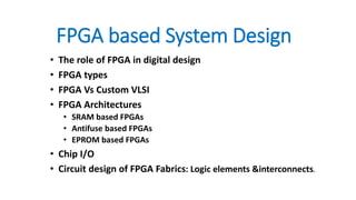
  • 1. FPGA based System Design • The role of FPGA in digital design • FPGA types • FPGA Vs Custom VLSI • FPGA Architectures • SRAM based FPGAs • Antifuse based FPGAs • EPROM based FPGAs • Chip I/O • Circuit design of FPGA Fabrics: Logic elements &interconnects.
  • 2. The role of FPGA in digital design • Field-programmable gate arrays (FPGAs) fill a need in the design space of digital systems, complementary to the role played by microprocessors. Microprocessors can be used in a variety of environments, but because they rely on software to implement functions, they are generally slower and more power-hungry than custom chips. • Similarly, FPGAs are not custom parts, so they aren’t as good at any particular function as a dedicated chip designed for that application. • FPGAs are generally slower and burn more power than custom logic. • FPGAs are also relatively expensive; it is often tempting to think that a custom-designed chip would be cheaper.
  • 3. The role of FPGA in digital design Advantages of FPGAs: 1. There is no wait from completing the design to obtaining a working chip. The design can be programmed into the FPGA and tested immediately. 2. FPGAs are excellent prototyping vehicles. When the FPGA is used in the final design, the jump from prototype to product is much smaller and easier to negotiate. 3. The same FPGA can be used in several different designs, reducing inventory costs.
  • 4. The role of FPGA in digital design • The area filled by FPGAs has grown enormously in the past twenty years since their introduction. • Programmable logic devices (PLDs) had been on the market since the early 1970s. These devices used two level logic structures to implement programmed logic. • The first level of logic, the AND plane, was generally fixed, while the second level, known as the OR plane, was programmable. PLDs are generally programmed by anti fuses, which are programmed through large voltages to make connections. • They were most often used as glue logic—logic that was needed to connect together the major components of the system.
  • 5. The role of FPGA in digital design • Two-level logic is useful for relatively small logic functions, but as levels of integration grew, two-level structures became too inefficient. • FPGAs provided programmable logic using multi-level logic of arbitrary depth. • They used both programmable logic elements and programmable interconnect to build the multi-level logic functions.
  • 6. The role of FPGA in digital design • Ross Freeman is generally credited with the invention of the FPGA. His FPGA included both programmable logic elements and a programmable interconnect structure. • His FPGA was also programmed using SRAM, not antifuses. • It also allowed the FPGA to be reprogrammed while it was in-circuit; this was a particularly interesting feature since flash memory was not yet in common use.
  • 7. The role of FPGA in digital design • Xilinx and Altera both sold early SRAM-based FPGAs. • An alternative architecture was introduced by Actel, which used an antifuse architecture. • This architecture was not reprogrammable in the field, which arguably was an advantage in situations that did not require reconfiguration. • The Actel FPGAs used a mux-oriented logic structure organized around wiring channels.
  • 8. The role of FPGA in digital design • For many years FPGAs were seen primarily as glue logic and prototyping devices. Today, they are used in all sorts of digital systems: 1. as part of high-speed telecommunications equipment; 2. as video accelerators in home personal video recorders (PVRs). • FPGAs have become mainstream devices for implementing digital systems.
  • 9. FPGA Types Here are some defining characteristics of FPGAs: 1. They are standard parts. They are not designed for any particular function but are programmed by the customer for a particular purpose. 2. They implement multi-level logic. The logic blocks inside FPGAs can be connected in networks of arbitrary depth. PLDs, in contrast, use two levels of NAND/NOR functions to implement all their logic.
  • 10. FPGA Types Here are some defining characteristics of FPGAs: 1. They are standard parts. They are not designed for any particular function but are programmed by the customer for a particular purpose. 2. They implement multi-level logic. The logic blocks inside FPGAs can be connected in networks of arbitrary depth. PLDs, in contrast, use two levels of NAND/NOR functions to implement all their logic.
  • 11. FPGA Types Here are some defining characteristics of FPGAs: 1. They are standard parts. They are not designed for any particular function but are programmed by the customer for a particular purpose. 2. They implement multi-level logic. The logic blocks inside FPGAs can be connected in networks of arbitrary depth. PLDs, in contrast, use two levels of NAND/NOR functions to implement all their logic. • Because FPGAs implement multi-level logic, they generally need both programmable logic blocks and programmable interconnect. PLDs use fixed interconnect and simply change the logic functions attached to the wires.
  • 12. FPGA Types • FPGAs, in contrast, require programming logic blocks and connecting them together in order to implement functions. • The combination of logic and interconnect is known as a fabric because it possesses a regular structure that can be efficiently utilized by design tools that map the desired logic onto the FPGA. • One of the major defining characteristics of the FPGA is that it can be programmed.
  • 14. FPGA Types • A computer system includes both a CPU and a separate memory that stores instructions and data. • The FPGA’s program is interwoven into the logic structure of the FPGA. • An FPGA does not fetch instructions—the FPGA’s programming directly implements logic functions and interconnections. • A variety of technologies are used to program FPGAs. Some FPGAs are permanently programmed; others can be reprogrammed. • Reprogrammable FPGAs are also known as reconfigurable devices.
  • 15. FPGA Types • Reconfigurable FPGAs are generally favored in prototype building because the device doesn’t need to be thrown away every time a change is made. • Reconfigurable systems can also be reprogrammed on-the-fly during system operation. • This allows one piece of hardware to perform several different functions • For example, the Radius computer display operated in both horizontal (landscape) and vertical (portrait) modes. When the user rotated the display, a mercury switch caused the FPGA that ran the display to be reprogrammed for the new mode.
  • 16. FPGA Types • Reconfigurable FPGAs are generally favored in prototype building because the device doesn’t need to be thrown away every time a change is made. • Reconfigurable systems can also be reprogrammed on-the-fly during system operation. • This allows one piece of hardware to perform several different functions • For example, the Radius computer display operated in both horizontal (landscape) and vertical (portrait) modes. When the user rotated the display, a mercury switch caused the FPGA that ran the display to be reprogrammed for the new mode.
  • 17. FPGA Types • FPGAs have traditionally used fine-grained logic. • A combinational logic element in a traditional FPGA implements the function of a handful of logic gates plus a register. • As chips become larger, coarser-grained FPGAs are coming into use. • A single logic element in these chips may implement a multi-bit ALU and register. • Coarser-grained FPGAs may make more efficient use of chip area for some types of functions.
  • 18. FPGA Types • A newer category of FPGAs includes more than just the FPGA fabric itself. Platform FPGAs include several different types of structures so that each part of a large system can be efficiently implemented on the type of structure best suited to it. • A platform FPGA typically includes a CPU so that some functions can be run in software. • It may also include specialized bus logic so that, for example, a PCI bus interface can easily be included into the system.
  • 19. FPGAs vs. Custom VLSI • The main alternative to an FPGA is an application-specific IC (ASIC). • Unlike an FPGA, an ASIC is designed to implement a particular logical function. • The design of an ASIC goes down to the masks used to fabricate an IC. The ASIC must be fabricated on a manufacturing line, a process that takes several months, before it can be used or even tested. • ASICs are typically distinguished from full custom designs: a full-custom design has a custom layout, while an ASIC uses pre-designed layout outs for logic gates. • Today, few large digital chips other than microprocessors include a significant amount of custom layout.
  • 20. FPGAs vs. Custom VLSI • ASICs have some significant advantages because they are designed for a particular purpose: they are generally faster and lower power than FPGA equivalents; when manufactured in large volumes, they are also cheaper. • However, two trends are leading many system designers to use FPGAs rather than ASICs for custom logic.
  • 21. FPGAs vs. Custom VLSI • On the one hand, Moore’s Law has provided substantial increases in the capacity of integrated circuits. Moore’s Law states that the number of transistors that can be manufactured on a chip will double every 18 months.
  • 22. FPGAs vs. Custom VLSI • With so many transistors on a single chip, it is often tempting—and increasingly necessary—to throw away transistors in order to simplify the task of designing the logic on the chip. • FPGAs use more transistors for a given function than do ASICs, but an FPGA can be designed in days. • On the other hand, the cost of the masks used to manufacture an ASIC is skyrocketing. • The basic figure of merit of an IC manufacturing line is the width of the smallest transistor it can build. • As line widths shrink, the cost of manufacturing goes up—a modern semiconductor manufacturing plant costs several billion dollars.
  • 23. FPGAs vs. Custom VLSI • As Table shows, the costs of masks are growing exponentially. As VLSI line widths shrink, mask costs will start to overshadowthe costs of the designers who create the chip. • As mask costs soar, standard parts become more attractive. • Because FPGAs are standard parts that can be programmed for many different functions, we can expect them to take a larger share of the IC market for high-density chips.
  • 24. FPGA Architectures • In general, FPGAs require three major types of elements: 1. combinational logic; 2. interconnect; 3. I/O pins.
  • 25. Interconnect may require complex paths
  • 26. SRAM-Based FPGAs • Static memory is the most widely used method of configuring FPGAs. • In this section we will look at the elements of an FPGA: logic, interconnect, and I/O. • SRAM-based FPGAs hold their configurations in static memory • The output of the memory cell is directly connected to another circuit and the state of the memory cell continuously controls the circuit being configured.
  • 27. SRAM-Based FPGAs Using static memory has several advantages: • The FPGA can be easily reprogrammed. Because the chips can be reused, and generally reprogrammed without removing them from the circuit, SRAM-based FPGAs are the generally accepted choice for system prototyping. • The FPGA can be reprogrammed during system operation, providing dynamically reconfigurable systems. • The circuits used in the FPGA can be fabricated with standard VLSI processes. • Dynamic RAM, although more dense, needs to be refreshed, which would make the configuration circuitry much more cumbersome. SRAM-based FPGAs also have some disadvantages: • The SRAM configuration memory burns a noticeable amount of power, even when the program is not changed. • The bits in the SRAM configuration are susceptible to theft.
  • 28. SRAM-Based FPGAs • The basic method used to build a combinational logic block (CLB)— also called a logic element or LE—in an SRAM-based FPGA is the lookup table (LUT). • As shown in Figure, the lookup table is an SRAM that is used to implement a truth table.
  • 29. SRAM-Based FPGAs • Each address in the SRAM represents a combination of inputs to the logic element. • The value stored at that address represents the value of the function for that input combination. • An n-input function requires an SRAM with locations. • Because a basic SRAM is not clocked, the lookup table LE operates much as any other logic gate—as its inputs change, its output changes after some delay.
  • 30. SRAM-Based FPGAs • Unlike a typical logic gate, the function represented by the LE can be changed by changing the values of the bits stored in the SRAM. • As a result, the n-input LE can represent 2^2^nfunctions (though some of these functions are permutations of each other). • A typical logic element has four inputs. • The delay through the lookup table is independent of the bits stored in the SRAM, so the delay through the logic element is the same for all functions. • This means that, for example, a lookup table based LE will exhibit the same delay for a 4-input XOR and a 4-input NAND. In contrast, a 4-input XOR built with static CMOS logic is considerably slower than a 4-input NAND.
  • 31. SRAM-Based FPGAs • Logic elements generally contain registers—flip-flops and latches—as well as combinational logic. • A flip-flop or latch is small compared to the combinational logic element so it makes sense to add it to the combinational logic element. • Using a separate cell for the memory element would simply take up routing resources.
  • 32. SRAM-Based FPGAs • As shown in Figure, the memory element is connected to the output; whether it stores a given value is controlled by its clock and enable inputs.
  • 33. SRAM-Based FPGAs • More complex logic blocks are also possible. For example, many logic elements also contain special circuitry for addition. • Many FPGAs also incorporate specialized adder logic in the logic element. • The critical component of an adder is the carry chain, which can be implemented much more efficiently in specialized logic than it can using standard lookup table techniques.
  • 35. SRAM-Based FPGAs Interconnection Networks: • Logic elements must be interconnected to implement complex machines. An SRAM-based FPGA uses SRAM to hold the information used to program the interconnect. As a result, the interconnect can be reconfigured, just as the logic elements can. • Following Figure shows a simple version of an interconnection point, often known as a connection box. • A programmable connection between two wires is made by a CMOS transistor (a pass transistor). The pass transistor’s gate is controlled by a static memory program bit
  • 36. SRAM-Based FPGAs • When the pass transistor’s gate is high, the transistor conducts and connects the two wires; when the gate is low, the transistor is off and the two wires are not connected. • A CMOS transistor has a good off-state • In this simple circuit, the transistor also conducts bidirectionally— it doesn’t matter which wire has the signal driver. • However, the pass transistor is relatively slow, particularly on a signal path that includes several interconnection points in a row. • There are several other circuits that can be used to build a programmable interconnection point, most of them unidirectional. • These alternative circuits provide higher performance at the cost of additional chip area.
  • 37. SRAM-Based FPGAs Performance: • FPGA wiring with programmable interconnect is slower than typical wiring in a custom chip for two reasons: the pass transistor and wire lengths. • The pass transistor is not a perfect on-switch, so a programmable interconnection point is somewhat slower than a pair of wires permanently connected by a via. • In addition, FPGA wires are generally longer than would be necessary for a custom chip. In a custom layout, a wire can be made just as long as necessary. • In contrast, FPGA wires must be designed to connect a variety of logic elements and other FPGA resources. • A net made of programmable interconnect may be longer, introducing extra capacitance and resistance that slows down the signals on the net.
  • 38. SRAM-Based FPGAs Configuration: • SRAM-based FPGAs are reconfigured by changing the contents of the configuration SRAM. • A few pins on the chip are dedicated to configuration; some additional pins may be used for configuration and later released for use as general- purpose I/O pins. • When we start up the system, we can usually tolerate some delay to download the configuration into the FPGA. • However, there are cases when configuration time is important. This is particularly true when the FPGA will be dynamically reconfigured— reconfigured on-the-fly while the system is operating, such as the Radius monitor described.
  • 40. f  x1x2  x2 x3 0 0 0 1 x1 x2 f1 0 1 0 0 x2 x3 f2 0 1 1 1 f1 f2 f3 x1 x2 x3 f f1  x1x2 f2  x2 x3 An example of programming an FPGA