
Recommandé
Contenu connexe
En vedette
En vedette (7)
Similaire à 100 sadanand v. deshpande - 7344983 - clustered surface preparation for silicide and metal contacts
Similaire à 100 sadanand v. deshpande - 7344983 - clustered surface preparation for silicide and metal contacts (20)
Plus de Mello_Patent_Registry
Plus de Mello_Patent_Registry (20)
Dernier
Dernier (20)
100 sadanand v. deshpande - 7344983 - clustered surface preparation for silicide and metal contacts
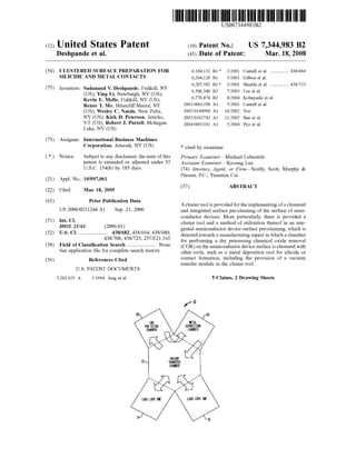
- 1. c12) United States Patent Deshpande et al. (54) CLUSTERED SURFACE PREPARATION FOR SILICIDE AND METAL CONTACTS (75) Inventors: Sadanand V. Deshpande, Fishkill, NY (US); Ying Li, Newburgh, NY (US); Kevin E. Mello, Fishkill, NY (US); Renee T. Mo, Briarcliff Manor, NY (US); Wesley C. Natzle, New Paltz, NY (US); Kirk D. Peterson, Jericho, VT (US); Robert J. Purtell, Mohegan Lake, NY (US) (73) Assignee: International Business Machines Corporation, Armonk, NY (US) ( *) Notice: Subject to any disclaimer, the term of this patent is extended or adjusted under 35 U.S.C. 154(b) by 183 days. (21) Appl. No.: 10/907,061 (22) Filed: Mar. 18, 2005 (65) Prior Publication Data US 2006/0211244 Al Sep. 21, 2006 (51) Int. Cl. HOJL 21144 (2006.01) (52) U.S. Cl. ...................... 438/682; 438/664; 438/680; 438/708; 438/723; 257/E21.165 (58) Field of Classification Search ..................... None See application file for complete search history. (56) References Cited U.S. PATENT DOCUMENTS 5,282,925 A 211994 Jeng et a!. 111111 1111111111111111111111111111111111111111111111111111111111111 US007344983B2 (10) Patent No.: (45) Date of Patent: US 7,344,983 B2 Mar.18,2008 6,184,132 B1 * 2/2001 Cantell eta!. .............. 438/664 6,204,120 B1 3/2001 Gilboa et al. 6,207,582 B1 * 3/2001 Shields et a!. .............. 438/723 6,586,340 B2 7/2003 Lee eta!. 6,776,874 B2 8/2004 Kobayashi et a!. 2001/0001298 A1 5/2001 Cantell eta!. 2002/0144904 A1 10/2002 Yoo 2002/0162742 A1 1112002 Bae eta!. 2004/0092101 A1 5/2004 Pyo eta!. * cited by examiner Primary Examiner-Michael Lebentritt Assistant Examiner-Kyoung Lee (74) Attorney, Agent, or Firm-Scully, Scott, Murphy & Presser, P.C.; Yuanmin Cai (57) ABSTRACT A cluster tool is provided for the implementing ofa clustered and integrated surface pre-cleaning of the surface of semi- conductor devices. More particularly, there is provided a cluster tool and a method of utilization thereof in an inte- grated semiconductor device surface pre-cleaning, which is directed towards a manufacturing aspect in which a chamber for performing a dry processing chemical oxide removal (COR) on the semiconductor device surface is clustered with other tools, such as a metal deposition tool for silicide or contact formation, including the provision of a vacuum transfer module in the cluster tool. 5 Claims, 2 Drawing Sheets
- 2. U.S. Patent Mar. 18, 2008 Sheet 1 of 2 12 COR PRE-ClEAN CHAMBER LOAD LOCK 0~ FIG. 1 VACLlJH TRANSFER CHAMBER METAL DEPOSITION CHAMBER LOAD LOCK TWO US 7,344,983 B2
- 3. U.S. Patent Mar. 18,2008 Sheet 2 of 2 34 FIG. 2 (PRIOR ART) NH3 NH3 IF'{ I Hf NH4F I(NH4)2S1FS US 7,344,983 B2
- 4. US 7,344,983 B2 1 CLUSTERED SURFACE PREPARATION FOR SILICIDE AND METAL CONTACTS BACKGROUND OF THE INVENTION 1. Field of the Invention 2 chamber is provided with a robot placing the wafer into and out ofeach chamber. There is no disclosure or suggestion of providing for a dry processing method comprising a chemi- cal oxide removal (COR) of a surface film in a cluster tool, as in the present invention so as to provide for surface preparation for silicide and metal contacts on semiconductor devices. Bae, eta!., U.S. Patent Publication No. 2002/0162742 A1, describes a cluster tool for forming semiconductor devices The present invention relates to a cluster tool for the implementing of a clustered and integrated surface pre- cleaning of the surface of semiconductor devices. More particularly, the invention is directed to the provision of a cluster tool and to a method of utilization thereof in an integrated semiconductor device surface pre-cleaning, which is directed towards a manufacturing aspect in which a chamber for performing a dry processing chemical oxide removal (COR) on the semiconductor device surface is clustered with other tools, such as a metal deposition tool for silicide or contact formation, including the provision of a vacuum transfer module in the cluster tool. 10 using a wafer process including at least one load port at which wafers are loaded and wherein a front end system uses an ATM (atmosphere) robot and ATM aligner. There is no disclosure of employing a vacuum transfer system and cluster tool for chemical oxide removal, nor a dry processing 15 operation to prepare a surface of a semiconductor device for silicide or metal contacts, as in the present invention. Yoo, U.S. Patent Publication No. 2002/0144904, dis- closes a processing system and related method for vacuum evaporation of a material layer or film on a substrate.Extensive experimentation and physical applications have been implemented in connection with the preparation of surfaces of semiconductor devices for the formation of silicide and metal contacts, employing so called cluster tools wherein, in particular, in order to effectuate the removal of surface films and thin layers of oxides, there are provided advantages in contrast with conventional wet etch based process flows. 20 However, although there is provision made for a series of pumps for selecting processing pressure levels without the need for lowering the pressure to deep vacuum pressure conditions, there is no disclosure of a dry processing cham- ber to provide for chemical oxide removal (COR), which is 25 clustered with other tools, so as to prepare a clustered surface for silicide or metal contact formation on a semi- Pursuant to the current state-of-the-art, which is con- cerned with various technical and economic aspects of semiconductor processing and manufacture, in order to fulfill a need for small or miniaturized geometries and 30 improved performance characteristics, the contact module has attained an increased significance as an important ele- ment of chip yield and semiconductor device performance. For instance, in the currently employed 65 nm and 45 nm technologies, the requirements for a high-strength and low- 35 resistance electrical path which make contact to the semi- conductor device, are criteria which define limitations in the performance of the device. Thus, in order to address the problems which are encoun- tered by such performance limitations, consideration can be 40 applied to techniques involving the applicability ofchemical oxide removal (COR) based processes to the removal of deleterious surface oxides on the semiconductor surfaces which may present an impediment to the enabling ofa good ohmic contact to semiconductor devices. In this connection, 45 the presence ofoxygen interfaces and oxygen contamination are serious problems encountered in contact module formu- lations and may result in significant performance and yield losses in advanced technology nodes. To a significant extent, this problem has been addressed in 50 U.S. Pat. Nos. 5,184,132 B1 and 5,282,925; and U.S. Patent Publication No. 2001/0001298 A1, all of which are com- monly assigned to the assignee of this application, and the contents of which are incorporated herein in their entireties; and wherein U.S. Pat. No. 5,282,925 is discussed in further 55 detail in connection with the present invention. 2. Discussion of the Prior Art Pyo, eta!., U.S. Patent Publication No. 2004/0092101 A1, discloses a Cu-thin film deposition equipment for a semi- conductor device, which is intended to improve the speed of 60 depositing a Cu-thin film, and resultingly lowering the corresponding manufacturing costs. Although there is pro- vided a load lock for carrying out the film deposition steps before and after wafer processes, and wherein an aligner effectuates alignments so that a wafer reaches a desired 65 position, a degassing chamber removes residue, such as gas produced on the surface of a wafer, whereas a feeding conductor device. Kobayashi, eta!., U.S. Pat. No. 6,776,874 B2 discloses a processing method and apparatus for removing oxide films from a surface ofan object which is to be treated through the intermediary ofvarious gas treatments. However, there is no disclosure of a cluster tool and method utilizing a dry processing chamber for chemical oxide removal, including a metal deposition tool with a vacuum transfer module pursuant to the present invention, adapted to prepare a surface for silicide or metal contact formation. Similarly, Lee, et a!., U.S. Pat. No. 6,586,340 B2 and Gilboa, et a!., U.S. Pat. No. 6,204,120 B1 disclose various pre-treatment methods for semiconductor wafers, and for subsequent processing, including transfer chambers and pluralities of vacuum conditions for removing native oxide films from the surface of a subject, such as cluster type wafers or the like. However, there is no description of a clustered surface preparation for silicide and metal films to form contacts in a dry process pre-cleaning (COR) operation using a clustered tool providing chemical oxide removal chambers and metal deposition chambers in conjunction with vacuum transfer chambers and load lock cluster arrangements, as is described by the present invention. SUMMARY OF THE INVENTION The present invention, in order to provide an advance in the processing of semiconductor devices, is, accordingly, directed to the provision of an integrated work tool and method for the clustered surface preparation of a semicon- ductor surface for the formation of silicide and metal con- tacts possessing low-resistance and high-ohmic electrical path characteristics. The inventive concept entails the utili- zation of the chemical oxide removal (COR) process of eliminating surface oxide films, such as native oxide, as an integrated process with coordinated subsequent metal depo- sitions for silicide or contact formation. Accordingly, in order to clearly distinguish and improve over the prior art, pursuant to the present invention, there is provided a cluster tool arrangement for a pre-cleaning oxide film removing surface preparation for enabling silicide and
- 5. US 7,344,983 B2 3 metal depositions on semiconductor devices by employing a cleaner integrated processing without a vacuum break and through an improved interface control. In particular, pursu- ant to the invention, the cluster tool arrangement replaces the current wet-etch based process flow by the provision ofa dry method of processing which reduces the usage of wet chemicals and enables a cleaner application for surface preparation prior to implementing any metal deposition. In particular, the invention utilizes a chemical oxide removal (COR) process and chamber, for instance, such as in U.S. Pat. No. 5,282,925; which selectively is employed among various types of oxides, such as native oxide, pos- sibly employing gaseous nitrogen trifluoride (NF3 ), or other gaseous mediums, which can conserve STI and control recess of the isolation so as to form improved silicides, for example, such as cobalt silicide, or suitable metals, such as titanium nitride, without any excessive STI oxide losses. Other patents and publications which are directed to the implementation of the COR process are U.S. Pat. No. 6,184,132 B1 and U.S. Patent Publication No. 2001/ 0001298 A1; which are commonly assigned to the present assignee, and the disclosures of which are incorporated herein in their entireties. 4 FIG. 2 illustrates, generally diagrammatically, an appara- tus for implementing the chemical oxide removal (COR) process, as known in the prior art. DETAILED DESCRIPTION OF THE INVENTION Referring to FIG. 1 of the drawings, there is diagram- matically illustrated a cluster tool arrangement 10, compris- 10 ing a vacuum transfer chamber 12, and providing for a first load lock 14 and a second load lock 16 for the transferring in and removal ofworkpieces, such as semiconductor wafers (not shown), which are to be pre-cleaned in a (COR) chamber 18 by means of a dry process consisting of chemi- 15 cal oxide removal (COR) methods, and then treated in a metal deposition chamber 20. The load-locks 14, 16; COR pre-cleaning chamber 18 and metal deposition chamber 20 are clustered about the vacuum through chamber 12. Referring, in particular, to the schematic representation, 20 as illustrated in FIG. 2 of the drawings, this discloses, diagrammatically, the pre-treatment chemical oxide removal (COR) chamber 18, which is employed in connection with the cluster tool arrangement 10, pursuant to the present invention. An even more specific advantage of the inventive dry 25 processing using COR over wet processing is a differentiator for SOl technologies and, in particular, where contact to Box leakage is a major concern. In this connection, the SOl structures include an insulating layer, in effect, a buried oxide region (BOX), which, for instance, electrically iso- 30 lates a top Si-containing layer from a bottom Si-containing layer, and wherein the top Si containing, or, in effect, the SOl layer serves as the area in which electronic devices, such as MOSFET (metal oxide semiconductor field effect transistor) devices are imparted a high degree of yield and efficiency. 35 In particular, the pre-treatment COR chamber 18, as diagrammatically disclosed herein, is described in detail in particular connection with FIG. 4 of Jeng, et a!., U.S. Pat. No. 5,282,925, which is commonly assigned to the present assignee, and the disclosure of which is incorporated herein in its entirety. In this connection, the CDR pre-treatment chamber 18 provides for a low-pressure and plasma-free and damage- free etching of silicon dioxide on a wafer surface, wherein the wafer is represented by reference numeral 30 in the drawing. Another improvement over the art provided for by the present invention relates to reduced queue times for pro- cessing lines, and improved raw processing times for the manufacture of contact and silicide modules. Accordingly, it is an object to provide an improved and novel clustered surface preparation tool for an oxide-remov- ing pre-cleaning and preparation for the silicide and metal contacts on semiconductor devices. Another object resides in the provision of a method of providing for a dry-process based chemical oxide removal method employed in the pre-treatment of clustered and integrated surfaces for silicide and metal contact preparation for semiconductor devices and modules. Hereby, the pre-treatment chamber 18 is provided with water through the passageway 32, wherein the wafer 30 is positioned on the upper surface of the support structure 34 and may be heated by means of a suitable heating arrange- 40 ment, such as coils 36 or the like. The pressure in the pre-treatment chamber 18 may be suitably controlled, as is described in the foregoing U.S. Pat. No. 5,282,925 and gaseous mixtures ofammonia (NH3 ) and hydrogen fluoride HF are injected into the interior of the 45 chamber 18 through respective inlet conduits 38 and 40. In effect, through suitably controlled pressure and tem- perature conditions, as described in U.S. Pat. No. 5,282,925, chemical oxide removal (COR) is implemented in an essen- tially two-step reaction in which in a first step, solid reaction 50 product (NH4 ) 2 SiF6 is formed on the oxide surface which is present on the wafer 30 and self limits the reaction. This enables a controlled removal of oxide for the wafer surface pre-clean preparation. Thereafter, in a second step, the Yet another object resides in the provision ofa cluster tool for the preparation of silicide and metal surfaces without a vacuum break and better interface control employing a cluster tool comprising a COR pre-clean chamber, a metal deposition chamber including a vacuum chamber in con- nection with a load lock for the rapid dry processing of 55 semiconductor surfaces. reaction product is removed through discharge sublets 42, 44 by heating (sublimation) responsive to the heat of the reaction being controlled (not shown) by a suitable control- BRIEF DESCRIPTION OF THE DRAWINGS Reference may now be made to the following detailed description of a preferred embodiment of the invention, taken in conjunction with the accompanying drawings, in which: FIG. 1 illustrates a cluster tool arrangement for the surface pre-cleaning of a semiconductor device in a COR chamber, and which is integrated with the preparation of silicide and metal contacts; and ler acting on heating coils 36, the latter of which are diagrammatically represented in the drawing. The particular conditions for the implementation of the 60 chemical oxide removal (CDR) process are detailed in the disclosure of U.S. Pat. No. 5,282,925 and a detailed repeti- tion thereof in the present specification is deemed to be unnecessary for an understanding of the invention. In particular, the cluster tool arrangement 10 provides for 65 a selective cleaning of different types of oxides from the surfaces of the semiconductor device or wafer so as to control and conserve STI oxide losses. Hereby, the semi-
- 6. US 7,344,983 B2 5 conductor device or wafer is transported into a respective load lock 14, 16, and from there into vacuum transfer chamber 12. Thereafter, under vacuum condition, the wafer (or semiconductor device) is conveyed into pre-cleaned chamber 18, which basically comprises the COR (chemical oxide removal) apparatus for effecting an oxide-removing cleaning sequence on the wafer surface. Upon completion of the removal of oxide film or surface deposition, the wafer is then transferred back to the vacuum transfer chamber 12 and then into metal deposition chamber 20, where the appropri- 10 ate metal deposition of silicides or other metals, as known, is imparted to the surface of the semiconductor device or wafer to produce the desired contacts possessing high- strength and high-ohmic electrical path characteristics. The wafer metal or silicide-forming surface preparation having 15 been completed, the wafer or semiconductor module is transferred back to the vacuum transfer chamber 12 and from there to one of the load locks 14 or 16 for further conveyance and processing at a further site in accordance with the prevailing technology. 20 While the present invention has been particularly shown and described with respect to preferred embodiments, it will be understood by those skilled in the art that the foregoing and other changes in forms and details may be made without departing from the spirit and scope of the present invention. 25 It is therefore intended that the present invention not be limited to the exact forms and details described and illus- trated, but fall within the scope of the appended claims. What is claimed is: 1. A method for the integrated pre-cleaning of a semicon- 30 ductor surface and surface preparation for forming metal and 6 silicide contacts thereon; wherein said method is imple- mented in a cluster tool for the removal of a dry chemical oxide by a gaseous medium operating under a vacuum condition; comprising a plurality of segmented steps of: providing a silicon semiconductor substrate having a native oxide film present on a surface thereof; uninterruptedly and continuously imparting said vacuum condition to said semiconductor surface during the implementation of said method having said oxide film thereon; performing said dry processing chemical oxide removal (COR) in a plasma-free application resulting in the absence of a plasma on said semiconductor surface for removing said native oxide film, while maintaining said vacuum condition so as to produce an oxygen-free semiconductor surface; and without breaking said vacuum condition in order to avoid an exposure of said surface to air, depositing a metal on said oxygen-free semiconductor surface and forming said silicide and metal contacts on said surface. 2. A method as claimed in claim 1, wherein said gaseous medium comprises nitrogen trifluoride (NF3 ). 3. A method as claimed in claim 1, wherein said metal is cobalt. 4. A method as claimed in claim 1, wherein said silicide is cobait silicide. 5. A method as claimed in claim 1, wherein said metal is titanium for forming a titanium nitride on said semiconduc- tor surface. * * * * *