A SURVEY OF DIFFERENT APPROACHES FOR OVERCOMING THE PROCESSOR-MEMORY BOTTLENECK
IEEExeonmem
1. MICHAEL E. THOMADAKIS 1
Memory Scalabilty and Performance in Intel64
Xeon SMP Platforms
MICHAEL E. THOMADAKIS
Abstract—
cc-NUMA systems based on the Intel Nehalem and the
Westmere processors are very popular with the scientific
computing communities as they can achieve high floating-
point and integer computation rates on HPC workloads.
However, a closer analysis of the performance in their
memory subsystem reveals that the per core and per thread
memory bandwidth of either microprocessor is restricted
to almost 1
3 of their ideal values. Multi-threaded memory
access bandwith tops out at 2
3 of the maximum limit. In
addition to this, the NUMA effect on latencies increasingly
worsens as cores try to access larger memory resident
data structures and the problem is exacerbated when the
regular 4KiB page sizes are used. Moving from Nehalem
to Westmere, read performance for data already owned
by the same core scales gracefully with the number of
cores and core clock speed. However, when data is within
the L2 cache or beyond, write performance suffers in
Westmere revealing scalability issues in their design when
the system from the 4 to 6 cores. This problem gets more
acute when multiple streams of data progress concurrently.
The Westmere memory subsystem compared to that of the
Nehalem, suffers from a worse performance degradation
when threads on a core are modifying cache blocks owned
by different cores within the same or another processor
chip. Applications moving from Nehalem to Westmere
based platforms, could experience unexpected memory
access degradation even though Westmere was intented
as a “drop-in” replacement for Nehalem.
In this work we attempt to provide an accurate account
of the on-chip and the system level bandwith and latency
limitations of Xeons. We study how these two metrics
scale as we move from one generation of a platform to
subsequent ones where the clock speed, the number of
cores and other architecture parameters are different.
Here we also analyze how much locality, coherence
state and virtual memory page size of data blocks affects
memory performance. These last three factors are tra-
ditionally overlooked, but if not given adequate attention
can affect application performance significantly. We believe
the performance analysis presented here can be used by
application developers who strive to tune their code to use
the underlying resources efficiently and avoid unecessary
bottlenecks or surprising slowdowns.
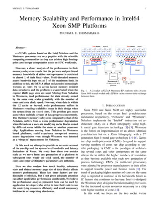
2. Fig. 1. A 2-socket ccNUMA Westmere-EP platform with a 6-core
Xeon 5600 in each socket and a QPI for cache coherent data exchange
between them.
I. INTRODUCTION
Xeon 5500 and Xeon 5600 are highly successful
processors, based on the recent Intel µ-architectures
nicknamed respectively, “Nehalem” and “Westmere”.
Nehalem implements the “Intel64” instruction set ar-
chitecture (ISA), on a 45nm lithography, using high-
k metal gate transistor technology [1]–[3]. Westmere
is the follow-on implementation of an almost identical
µ-architecture but on a 32nm lithography, with a 2nd
generation high-k metal gate technology [3]–[5]. Xeons
are chip multi-processors (CMPs) designed to support
varying numbers of cores per chip according to spe-
cific packaging. A CMP is the paradigm of architect-
ing several cores and other components on the same
silicon die to utilize the higher numbers of transistors
as they become available with each new generation of
process technology. CMPs (or multi-core processors)
were adopted by processor manufacturers in their effort
to support feasible power and thermal limits [6]. The
trend of packaging higher numbers of cores on the same
chip is expected to continue in the foreseeable future as
IC feature size continues to decrease. Intel co-designed
the Westmere chip alongside Nehalem making provisions
for the increased system resources necessary in a chip
with higher number of cores [4].
In this work we focus on the two socket 4-core
3. MICHAEL E. THOMADAKIS 2
Xeon 5500 (“Nehalem-EP”) and 6-core Xeon 5600
(“Westmere-EP”) platforms. Fig. 1 illustrates the basic
system components of the 12-core Westmere-EP plat-
form. Nehalem-EP platforms have an almost identical
system architecture but with 4 cores per chip. Other
differences between them will be discussed in later
sections.
Xeons have been employed extensively in high-
performance computing (HPC) platforms1
as they
achieve high floating-point and integer computation
rates. Xeons’ high-performance is attributed to a number
of enabling technologies incorporated in their design. At
the µ-architecture level they support, among others, spec-
ulative execution and branch-prediction, wide decode
and issue instruction pipelines, multi-scalar out-of-order
execution pipelines, native support for single-instruction
multiple-data (SIMD) instructions, simultaneous multi-
threading and support for a relatively high degree of
instruction level parallelism [3], [9]–[11].
Scientific applications usually benefit by higher num-
bers of execution resources, such as floating point or
integer units. These are available in the out-of-order,
back-end execution pipeline on Xeon cores. However,
in order to sustain high instruction completion rates,
the memory subsystem has to provide each core with
data and instructions at rates that will keep the pipeline
units utilized most of the time. The demand to feed the
pipelines is exacerbated in multi-core systems like the
Xeons, since the memory system has to keep up with
several cores simultaneously. Memory access is almost
always in the critical path of a computation. Clever
techniques are being devised on the architecture side to
mitigate the memory performance bottleneck.
Xeons rely on a number of modern architectural
features to speed up memory access by the cores. These
include an on-chip integrated memory controller (IMC),
multi-level hardware and software pre-fetching, deep
queues in load and store buffers, store-to-load forward-
ing, three levels of cache, two levels of Translation-
Lookaside Buffers, wide data paths, and high-speed
cache coherent inter-chip communication over the QPI
fabric [12], [13]. The on-chip integrated memory con-
troller attaches a Xeon chip to a local DRAM through
three independent DDR3 memory channels which for
Westmere can go up to 1.333GTransfers/s. On the
Xeon-EP platform each one of the two processor chips
directly connects to physically distinct DRAM space
forming a cache-coherent Non-Uniform Memory Access
1
Xeon processors power 65% and 55% of the HPC systems
appearing respectively, in the June 2011 [7] and the Nov. 2010 “Top-
500” lists [8].
(ccNUMA) system. Fig. 1 illustrates the cc-NUMA EP
organization with two processor sockets, separate on-
chip IMC and DRAM per socket and the physical
connectivity of the two sockets by the QPI. Separate
memory controllers per chip support increased scalability
and higher access bandwidths than were possible before
with older generations of Intel processors which relied
on the (in)famous Front Side Bus architecture.
A. Motivation for this Study
Even though great progress has been achieved with
Xeons in speeding up memory access, a closer per-
formance analysis of the memory subsystem reveals
that, the per core and per thread memory bandwidth of
either microprocessor is restricted to almost one third
of their theoretical values. The aggregate, multi-threaded
memory access bandwidth tops out at two thirds of the
maximum limit. In addition to this, the NUMA effect
on latencies increasingly worsens as cores try to access
larger memory-resident data structures and the problem
is exacerbated when the regular 4KiB page sizes are
used. The Westmere memory subsystem compared to
that of the Nehalem, suffers from a worse performance
degradation when threads on a core are writing to cache
blocks owned by different cores within the same chip or
another processor chip.
Moving from Nehalem to Westmere, read performance
for data already owned by the same core scales grace-
fully with the number of cores and core clock speed.
However, when data is within the L2 cache or beyond,
write performance suffers in Westmere revealing scala-
bility issues in their design when the system moved from
the 4 to 6 cores. Applications moving from Nehalem to
Westmere based platforms, could experience unexpected
memory access degradation even though Westmere was
intended as a “drop-in” replacement for Nehalem.
Application developers are faced with several chal-
lenges trying to write efficient code for modern multi-
core cc-NUMA platforms, such as those based on Xeon.
Developers now typically have to partition the computa-
tion into parallel tasks which should utilize the cores
and memory efficiently. The cost of memory access
is given special attention since memory may quickly
become the bottleneck resource. Developers implement
cache-conscious code to maximize reuse of data already
cached and avoid costlier access to higher levels in
the memory hierarchy. Another approach to increase
efficiency of multi-threaded applications, such as OMP
code in scientific applications, is to fix the location of
computation thread to a particular core and allocate data
elements from a particular DRAM module. Selecting the
4. MICHAEL E. THOMADAKIS 3
right location to place threads and data on particular
system resources is a tedious and at times lengthy trial
and error process. When memory access cost changes
the code has to be re-tuned.
This work attempts to accurately quantify memory
access cost by a core to memory locations which are
resident in the different levels of memory hierarchy
and owned by threads running on the same or other
cores. We analyze performance scalability limits as we
move from one generation of a platform to subsequent
ones where the clock speed, the number of cores and
other architecture parameters are different. The analysis
presented here can be used by application developers
who strive to understand resource access cost and tune
the code to use the underlying resources efficiently.
B. Related Work
Babka and T˚uma [14] attempted to experimentally
quantify the operating cost of Translation Lookaside
Buffers (TLBs) and cache associativity. Peng et al. [15]
used a “ping-pong” methodology to analyze the latency
of cache-to-cache transfers compare the memory per-
formance of older dual-core processors. The well-know
STREAM benchmark [16] measures memory bandwidth
at the user level but it disregards the impact in perfor-
mance of relevant architectural features, such as, NUMA
memory. Molka and Hackenberg [17], [18] compared
the latency and bandwidth of the memory subsystem on
AMD Shanghai and Intel Nehalem when memory blocks
are in different cache coherency states.
II. XEON MEMORY IDEAL PERFORMANCE LIMITS
Ideal data transfer figures are obtained by multiplying
the transfer rates times the data width in bits of each
system channel. Vendors, usually, publish this and other
more intimate design details partially2
.
Xeon processors chips consist of two parts, the “Core”
and the “Un-core,” which operate on separate clock
and power domains. Fig. 2 illustrates a 6-core West-
mere chip, the Core and Un-core parts, intra-chip data
paths and some associated ideal date transfer rates. The
un-core consists of the Global Queue, the Integrated
Memory Controller, a shared Level 3 cache and QPI
ports connecting to the other processor chip and to
I/O. It also contains performance monitoring and power
management logic. The Core part houses the processor
cores.
20. #!
*
-.
Fig. 3. Detail of the Global Queue, the connectivity to IMC, L3, the
cores and the QPI on a 4-core Nehalem chip, and associated ideal
transfer rates.
A. The “Un-Core” Domain
The Un-core clock usually operates at twice the speed
of the DDR3 channels and for our discussion we will
assume it is at 2.667GHz. The L3 on Xeon-EP platforms
supports 2MiB per core, which is 8MiB and 12MiB for
the Nehalem and Westmere, respectively. The L3 has
32-Byte read and write ports and operates on the Un-
core clock. The QPI subsystem operates on a separate
fixed clock which for the systems we will be considering
supports 6.4giga-transfers/s. The “Global Queue” (GQ)
structure is the central switching and buffering mech-
anism that schedules data exchanges among the cores,
the L3, the IMC and the QPI. Fig. 3 illustrates GQ
details on a Nehalem chip. The GQ buffers requests
from the Core for memory reads, for write-backs to
local memory and remote peer operations with 32, 16
and 12 slot entries, respectively. The GQ plays a central
2
[19] offers a more complete discussion of the memory architec-
ture on Nehalem-EP platforms and ideal performance figures which
also apply to Westmere-EP.
45. Fig. 4. Cache hierarchy and ideal performance limits in a Xeon
core.
role in the the operations and performance of the entire
chip [20]. However, few technical details are available
concerning GQ. Westmere increased the peak CPU and
I/O bandwidth to DRAM memory by increasing the
per socket un-core buffers to 88 from 64 in Nehalem
[4]. This “deeper” buffering was meant to support more
outstanding memory access operations per core than
possible in Nehalem-EP.
Ideally, the IMC can transfer data to the locally
attached DRAM at the maximum aggregate bandwidth
of the DDR3 paths to the memory DIMMs. The three
DDR3 channels to local DRAM support a bandwidth of
31.992GB/s = 3×8×1.333giga-transfers/s. Each core
in a socket should be able to capture a major portion of
this memory bandwidth.
The QPI links are full-duplex and their ideal transfer
rate is 12.8 GB/s per direction. When a core accesses
memory locations resident at the DRAM attached to the
other Xeon chip (see Fig. 1), data is transferred over
the QPI link connecting the chips together. The available
bandwidth through the QPI link is approximately %40 of
the theoretical bandwidth to the local DRAM and is the
absolute upper bound to access remote DRAM. The QPI,
L3, GQ and IMC include logic to support the “source-
snooping” MESIF-QPI cache-coherence protocol thatthe
Xeon-EP platform [12], [13] employs. The QPI logic
uses separate virtual channels to transport data or cache-
coherence messages according to their type. It also
pre-allocates fixed numbers of buffers for each source-
destination QPI pair. This likely exacerbates congestion
between end-points with high traffic.
B. The “Core” Domain
On the Core domain, each core supports two levels
of cache memory, L1 instruction and data, and a unified
L2. Fig. 4 presents details of the cache memory hierar-
chy, associated connectivity and some ideal performance
levels in a Nehalem core. Structure of Westmere cores
is very similar. The L2s connect to the L3 which is
shared by all cores, via the GQ structure. Each core has 2
levels of TLB structures for instructions and one for data.
There are separate TLBs for 4KiB and 2MiB size pages.
Each core includes a “Memory Order Buffer” with 48,
32 and 10 load, store and fill buffers, respectively. Fill
buffers temporarily store new incoming cache blocks.
There can be at most ten cache misses in progress at
a time, placing an upper bound on data retrieval rates
per core. All components in the Core domain operate on
the same clock as the processor. This implies that ideal
transfer rates scale with the clock frequency.
III. XEON MEMORY SYSTEM SCALABILITY
ANALYSIS
A. Design of Experiments
In this Section we analyze performance and scalabil-
ity limits in the Xeon and the EP platforms memory
systems. Conventional performance evaluations measure
memory bandwidth and latency regardless of (a) locality
or residency, that is, where this data is cached or reside
and (b) the cache coherence state it is on at the time of
the access. Another factor which is usually overlooked
is (c), the virtual memory page size the system is using
to map virtual addresses3
into physical ones.
In our analysis we take all of these aspects into ac-
count since, as we show, bandwidth performance figures
vary drastically with locality and cache state. Page size
affects mostly latency and to a smaller extend bandwidth.
Application developers along with the conventional
raw performance and scalability limits, also have to pay
increased attention to data locality and coherence state
and select a more proper page size to tune their code
accordingly.
We refer to Fig. 1 to illustrate details of our inves-
tigation applying to all of our experiments. We divide
the investigation into single-core and aggregate, multi-
core performance analysis. The single core focuses on
bandwidth and latency figures a single thread, that is
fixed on a particular physical core, experiences while ac-
cessing memory. The multi-core focuses on the aggregate
system-level performance figures when threads on every
core are all performing the same memory operation.The
3
The term “effective address” is used for this address.
46. MICHAEL E. THOMADAKIS 5
latter one evaluates how well contention for common
resources is handled by the architecture and it reveals
limitations and opportunities.
A single-core access pattern pins a software thread
on Core 1 (or “CPU 0”) and evaluates the bandwidth
accessing data on the L1 and L2 cache memories belong-
ing to the same core and on the L1 and L2 memories
belonging to each one of the other cores. It also evaluates
the bandwidth accessing data on the L3 and the DRAMs
attached to the same and to the other processor chips.
One each of the experiments the cache blocks the
threads access can be in different coherence states per
the MESIF-QPI protocol. We investigate the scalability
as we move from 4-core Nehalem to 6-core Westmere
processors and as we move from cores running at a
certain frequency to cores running at higher frequencies.
Wherever possible, we compare the attained performance
with the ideal performance numbers in that platform and
discuss its dependence on locality and on the particular
coherence state.
We have selected three different Xeon platform con-
figurations on two different working systems. All three
configurarions operate in the so called “IA-32e, full 64-
bit protected sub-mode” [9] which is the fully Intel64
compliant 64-bit mode.
The first system is an IBM iDataPlex cluster
called “Eos”, maintained by the Supercomputing
Facility at Texas AM University [21]. Eos con-
sists of a mixture of Nehalem-EP (Xeon-5560) and
Westmere-EP (Xeon-5660) nodes, with all cores running
at 2.8GHz. Each node has 24GiBs of DDR3 DRAM
operating at 1.333 GT/s.
The second system is Dell PowerEdge M610 blade
cluster, called “Lonestar” and is a maintained by the
Texas Advanced Computing Center (TACC) in the Uni-
versity of Texas at Austin. Lonestar consists only of
Westmere-EP (Xeon-5680) nodes with cores running
at 3.33GHz. Each node has 24GiBs of DDR3 DRAM
operating at 1.333 GT/s.
For all experiments we utilize the “BenchIT” [22],
[23] open source package4
which was built on the target
Xeon EP systems. We used a slightly modified version
of a collection of benchmarks called “X86membench”
[18]. These kernels use Intel64 assembly instructions to
read and write to memory and obtain timming measure-
ments using the “Cycle-counter” hardware register that
is available on each Xeon core.
B. Xeon Memory Bandwidth Analysis
4
Official web site of the BenchIt project at http://www.benchit.org.
5
10
15
20
25
30
35
40
45
10k 100k 1M 10M 100M 1G
bandwidth[GB/s]
data set size [Byte]
new_arch_x86_64.memory_bandwidth.C.pthread.SSE2.single-reader
read bandwidth CPU0 locally
read bandwidth CPU0 accessing CPU2 memory
read bandwidth CPU0 accessing CPU3 memory
read bandwidth CPU0 accessing CPU4 memory
read bandwidth CPU0 accessing CPU5 memory
read bandwidth CPU0 accessing CPU6 memory
read bandwidth CPU0 accessing CPU7 memory
Fig. 5. Bandwidth of a Single Reader Thread, Nehalem-EP, 4KiB
Pages (EOS)
1) Single Core Data Retrieval: In this experiment we
investigate the effective data retrieval rates by a single
core from the different levels of memory hierarchy and
all possible data localities in the system. This captures
the portion of the system capacity a single core can
utilize effectively. A single reader thread is pinned on
“CPU0” (core 1 in Fig. 1) and reads memory seg-
ments with sizes varying successively from 10KiBs to
200MiBs.
The reader thread retrieves memory blocks from its
own data L1 and L2 caches, then from the L3 and the
DRAM associated with its own processor chip. It then
retrieves data already cached on the L1, L2 of all other
cores on the same chip. Finally it retrieves data cached
on the L1, L2 of all cores, the L3 and DRAM associated
with the other processor chip.
All memory blocks, if already cached, are in the
“Exclusive” MESIF-QPI state in the corresponding own-
ing core. A data block enters this state when it has
been read and cached by exactly one core. By the QPI
protocol, a requested block may be retrieved directly out
of an L3 instead of each home DRAM, if is already
cached on that L3. As soon as a second core caches
a data block, the state of the first copy changes to
“Shared” and the state in the newly cached one becomes
“Forwarding”. MESIF protocol allows exactly one copy
to be in the latter state permitting it to quickly forward
it to the next requestor. This operation avoids accessing
the slower home memory and is called a “cache to cache
intervention”.
Fig. 5, Fig. 7 and Fig. 9 plot data retrieval bandwidths
on Nehalem and Westmere parts of EOS and on Lones-
tar, respectively. The top curves plot the BW in GiB/s
when the core retrieves data from its own L1, L2, L3 and
DRAM associated with its own and the remote chip. The
observed bandwidths of 43.7 GB/s, 43.6 GB/s and 51.8
47. MICHAEL E. THOMADAKIS 6
5
10
15
20
25
30
35
40
45
10k 100k 1M 10M 100M 1G
bandwidth[GB/s]
data set size [Byte]
new_arch_x86_64_LP.memory_bandwidth.C.pthread.SSE2.single-reader
read bandwidth CPU0 locally
read bandwidth CPU0 accessing CPU2 memory
read bandwidth CPU0 accessing CPU3 memory
read bandwidth CPU0 accessing CPU4 memory
read bandwidth CPU0 accessing CPU5 memory
read bandwidth CPU0 accessing CPU6 memory
read bandwidth CPU0 accessing CPU7 memory
Fig. 6. Bandwidth of a Single Reader Thread, Nehalem-EP, 2MiB
Pages (EOS)
5
10
15
20
25
30
35
40
45
10k 100k 1M 10M 100M 1G
bandwidth[GB/s]
data set size [Byte]
new_arch_x86_64.memory_bandwidth.C.pthread.SSE2.single-reader
read bandwidth CPU0 locally
read bandwidth CPU0 accessing CPU2 memory
read bandwidth CPU0 accessing CPU3 memory
read bandwidth CPU0 accessing CPU4 memory
read bandwidth CPU0 accessing CPU5 memory
read bandwidth CPU0 accessing CPU6 memory
read bandwidth CPU0 accessing CPU7 memory
read bandwidth CPU0 accessing CPU8 memory
read bandwidth CPU0 accessing CPU9 memory
read bandwidth CPU0 accessing CPU10 memory
read bandwidth CPU0 accessing CPU11 memory
Fig. 7. Bandwidth for a Single Reader Thread, Westmere-EP, 4KiB
Pages (EOS)
5
10
15
20
25
30
35
40
45
10k 100k 1M 10M 100M 1G
bandwidth[GB/s]
data set size [Byte]
new_arch_x86_64_LP.memory_bandwidth.C.pthread.SSE2.single-reader
read bandwidth CPU0 locally
read bandwidth CPU0 accessing CPU2 memory
read bandwidth CPU0 accessing CPU3 memory
read bandwidth CPU0 accessing CPU4 memory
read bandwidth CPU0 accessing CPU5 memory
read bandwidth CPU0 accessing CPU6 memory
read bandwidth CPU0 accessing CPU7 memory
read bandwidth CPU0 accessing CPU8 memory
Fig. 8. Bandwidth of a Single Reader Thread, Westmere-EP, 2MiB
Pages (EOS)
5
10
15
20
25
30
35
40
45
50
55
10k 100k 1M 10M 100M 1G
bandwidth[GB/s]
data set size [Byte]
new_arch_x86_64.memory_bandwidth.C.pthread.SSE2.single-reader
read bandwidth CPU0 locally
read bandwidth CPU0 accessing CPU2 memory
read bandwidth CPU0 accessing CPU3 memory
read bandwidth CPU0 accessing CPU4 memory
read bandwidth CPU0 accessing CPU5 memory
read bandwidth CPU0 accessing CPU6 memory
read bandwidth CPU0 accessing CPU7 memory
read bandwidth CPU0 accessing CPU8 memory
read bandwidth CPU0 accessing CPU9 memory
read bandwidth CPU0 accessing CPU10 memory
read bandwidth CPU0 accessing CPU11 memory
Fig. 9. Bandwidth for a Single Reader Thread, Westmere-EP, 4KiB
Pages (LoneStar)
accessing L1 cache (32 KiB) is very close to the ideal
ones. The ideal L1 BW for a 2.8GHZ and a 3.33GHz
Xeon is 44.8 GB/s (44.8GB/s = 2.8GHz × 16bytes)
and 53.28 GB/s (44.8GB/s = 3.33GHz × 16bytes),
respectively.
The L2 bandwidths are measured to 29.7 GB/s, 29.7
GB/s and 35.3, respectively. The vendor does not provide
figures on L2 performance except from the latency to
retrieve an L2 block.
Data retrievals scale well when we move from 4 cores
to 6 cores and also they scale well with the clock of core.
For instance we can check that 3.33
2.8 29.7 = 35.32 which
matches the measured L2 bandwidth on the Westmere
running at 3.33GHz.
L3 data retrieval figures are not provided by the vendor
and are measured to 23.8 GB/s, 23.1 GB/s and 25.6,
respectively. We notice that 3.33
2.8 25.6
23.1, implying that
L3 access does not scale linearly with the core clock.
This is expected since the L3 is at the Un-Core which
operates at twice the DDR3 rates.
The local DRAM supports 11.8 GB/s, 10.9 GB/s
and 11.1, respectively. The Remote DRAM supports 7.8
GB/s, 7.7 GB/s and 7.7, respectively. Data from remote
DRAM traverse the QPI link but the QPI ideal rate does
not appear to be the limiting factor.
The curves at the middle of the Fig. 5, Fig. 7 and
Fig. 9 plot retrieval rates of data items already cached
in the L1 or L2 of other cores within the same chip.
L3 which is an inclusive cache also caches whatever
is cached above in a L2 or L1. Thus L3 uses cache
intervention to pass a copy of this block up to core 1.
This explains why accessing data already cached by oter
cores has the same performance as accessing data from
the L3. Comparing 4-core and 6-core systems we see
that performance accessing blocks cached by other cores
within the same chip is worse for the 6-core system.
48. MICHAEL E. THOMADAKIS 7
5
10
15
20
25
30
35
40
45
10k 100k 1M 10M 100M 1G
bandwidth[GB/s]
data set size [Byte]
new_arch_x86_64.memory_bandwidth.C.pthread.SSE2.single-writer
memory bandwidth: CPU0 writing memory used by CPU0
memory bandwidth: CPU0 writing memory used by CPU2
memory bandwidth: CPU0 writing memory used by CPU3
memory bandwidth: CPU0 writing memory used by CPU4
memory bandwidth: CPU0 writing memory used by CPU5
memory bandwidth: CPU0 writing memory used by CPU6
memory bandwidth: CPU0 writing memory used by CPU7
Fig. 10. Bandwidth of Single Writer Thread, Nehalem-EP, 4KiB
Pages (EOS)
Finally the bottom curves show the rate for when core
1 access blocks already cached by cores on the other
chip. Rates start for all cases at around 9 GB/s where
data is supplied by the remote L3 and drop to around
7.7 GB/s for larger requests where the remote DRAM
has to be accessed.
The same experiment has been carried out with 2MiB
large VM pages on the Nehalem and Westmere parts
of EOS. Fig. 6 and Fig. 8 plot the respective results.
Bandwidth figures using large pages are similar to those
of the regular 4KiB pages with the only difference that
performance starts dropping a little later as we cross
boundaries in the memory hierarchies.
Overall, measured data retrieval rates are close to the
ideal limits and scale well with clock rate and as we
move from 4 to 6 cores.
It is clear that a single core cannot utilize the entire
available bandwidth to the DRAM. Resource limits along
the path from a core’s Memory Order Buffer to the IMC
are creating this artificial upper bandwidth bound. The
difference in bandwidth quickly deterriorates when the
cache memories cannot absorb the requests. Application
developers need to take this large performance disparities
when they tune their code for the architecture.
2) Single Core Data Updates: This experiment is the
data modification counterpart of the previous experiment
where the writer thread is also pinned on Core 1. All
blocks are initialized to the state “Modified” before the
measurements.
When a core has to write to a data block, the
MESIF protocol requires a “Read-for-Ownership” oper-
ation which snoops and invalidates this memory block if
it is already stored on other caches.
Fig. 10, Fig. 11 and Fig. 12 plot measured bandwidths.
The L1 rates closely match the retrieval rates. Perfor-
mance of L2 and L3 is relatively worse than when data
5
10
15
20
25
30
35
40
45
10k 100k 1M 10M 100M 1G
bandwidth[GB/s]
data set size [Byte]
new_arch_x86_64.memory_bandwidth.C.pthread.SSE2.single-writer
memory bandwidth: CPU0 writing memory used by CPU0
memory bandwidth: CPU0 writing memory used by CPU2
memory bandwidth: CPU0 writing memory used by CPU3
memory bandwidth: CPU0 writing memory used by CPU4
memory bandwidth: CPU0 writing memory used by CPU5
memory bandwidth: CPU0 writing memory used by CPU6
memory bandwidth: CPU0 writing memory used by CPU7
memory bandwidth: CPU0 writing memory used by CPU8
memory bandwidth: CPU0 writing memory used by CPU9
memory bandwidth: CPU0 writing memory used by CPU10
memory bandwidth: CPU0 writing memory used by CPU11
Fig. 11. Bandwidth of a Single Writer Thread, Westmere-EP, 4KiB
Pages (EOS)
5
10
15
20
25
30
35
40
45
50
55
10k 100k 1M 10M 100M 1G
bandwidth[GB/s]
data set size [Byte]
new_arch_x86_64.memory_bandwidth.C.pthread.SSE2.single-writer
memory bandwidth: CPU0 writing memory used by CPU0
memory bandwidth: CPU0 writing memory used by CPU2
memory bandwidth: CPU0 writing memory used by CPU3
memory bandwidth: CPU0 writing memory used by CPU4
memory bandwidth: CPU0 writing memory used by CPU5
memory bandwidth: CPU0 writing memory used by CPU6
memory bandwidth: CPU0 writing memory used by CPU7
memory bandwidth: CPU0 writing memory used by CPU8
memory bandwidth: CPU0 writing memory used by CPU9
memory bandwidth: CPU0 writing memory used by CPU10
memory bandwidth: CPU0 writing memory used by CPU11
Fig. 12. Bandwidth of a Single Writer Thread, Westmere-EP, 4KiB
Pages (LoneStar)
is retrieved from these caches. Local and remote DRAM
access is even worse. Writing local DRAm is 8.8 GB/s,
7.7 GB/s and 8.2 GB/s. Writing to remote DRAM on is
at around 5.5 for all three cases.
On 6-core systems writing to blocks already cached by
other cores on the same chip is a less scalable operation
than on a 4-core system. For instance Fig. 10 shows that
on the 4-core Nehalem the L3 can absorb gracefully all
block updates from within the same chip to a stable per-
formance of 17.6 GB/s. However, as we see on Fig. 11
and Fig. 12, the same scenario on the 6-core Westmere
attains 15.5 GB/s and 16.9 GB/s, respectively. The last
figure comes from a systems which operates at 3.33GHz,
that is 1.19 = 3.33
2.8 faster. However, the 2.8GHz Nehalem
still manages to attain 17.6 GB/s. More importandly, on
the 6-core systems the top curve (accessing data only
cached by itself) quickly deterriorates to 12.9 GB/s and
to even below 10 GB/s. The same curve on the 4-core
nehalem attains 17.6 GB/s and it appears much more
stable.
Applications moving from 4-core to 6-core systems
will experience unexpected performance degradation.
49. MICHAEL E. THOMADAKIS 8
0
10
20
30
40
50
60
70
80
10k 100k 1M 10M 100M 1G
bandwidth[GB/s]
data set size [Byte]
new_arch_x86_64.memory_bandwidth.C.pthread.SSE2.single-r1w1
bandwidth: CPU0 - CPU0
bandwidth: CPU0 - CPU2
bandwidth: CPU0 - CPU3
bandwidth: CPU0 - CPU4
bandwidth: CPU0 - CPU5
bandwidth: CPU0 - CPU6
bandwidth: CPU0 - CPU7
Fig. 13. Bandwidth of a Single Pair of Reader and Writer Streams,
Nehalem-EP, 4KiB Pages (EOS)
0
10
20
30
40
50
60
70
80
10k 100k 1M 10M 100M 1G
bandwidth[GB/s]
data set size [Byte]
new_arch_x86_64.memory_bandwidth.C.pthread.SSE2.single-r1w1
bandwidth: CPU0 - CPU0
bandwidth: CPU0 - CPU2
bandwidth: CPU0 - CPU3
bandwidth: CPU0 - CPU4
bandwidth: CPU0 - CPU5
bandwidth: CPU0 - CPU6
bandwidth: CPU0 - CPU7
bandwidth: CPU0 - CPU8
bandwidth: CPU0 - CPU9
bandwidth: CPU0 - CPU10
bandwidth: CPU0 - CPU11
Fig. 14. Bandwidth of a Single Pair of Reader and Writer Streams,
Westmere-EP, 4KiB Pages (EOS)
The hardware provisions made at design time moving
from 4 to 6 cores per chip restrict the scalability and
performance.
3) Combined Retrieval and Update – Single Stream
Pair: In this experiment, a single thread pinned on a
core, drives simultaneously a retrieval and an update
5
10
15
20
25
30
35
40
45
50
55
10k 100k 1M 10M 100M 1G
bandwidth[GB/s]
data set size [Byte]
new_arch_x86_64.memory_bandwidth.C.pthread.SSE2.single-r1w1
bandwidth: CPU0 - CPU0
bandwidth: CPU0 - CPU2
bandwidth: CPU0 - CPU3
bandwidth: CPU0 - CPU4
bandwidth: CPU0 - CPU5
bandwidth: CPU0 - CPU6
bandwidth: CPU0 - CPU7
bandwidth: CPU0 - CPU8
bandwidth: CPU0 - CPU9
bandwidth: CPU0 - CPU10
bandwidth: CPU0 - CPU11
Fig. 15. Bandwidth of a Single Pair of Reader and Writer Streams,
Westmere-EP, 4KiB Pages (LoneStar)
stream from various localities in the memory hierarchy
towards its local DRAM. This investigates the ability
of the memory to simultaneously retrieve and update
different locations. The bandwidth figures reflect the fact
that each data block is used in two memory operations.
Fig. 13, Fig. 14 and Fig. 15 plot measured bandwidths
from the three experimental configurations. The top
curves plot the case where both read and write streams
are on the same DRAM module. For data that can fit in
the L1s we attain 75.6GB/s, 75.8 GB/s and 53.3 GB/s,
respectively. This shows that the two ports of the L1 can
be used simultaneously and attain respectable rates. The
curves in the middle plot when the source is cached on
the L1 and L2 caches of cores within the same chip. The
bottom curves plot the bandwidths attained by moving
blocks cached or resident on the other chip’s localities.
However, since the cache memories end up caching two
copies of a data block, performance drops much faster
as soon as 1
2 of a cache is filled with the inbound
blocks. The two EOS configurations have approximately
the same performance, with the Westmere one having
somewhat lower levels. The LoneStar system appears to
perform with this workload in a more unstable fashion
as soon as the L1 is overwhelmed by inbound and
outbound copies with bandwidth dropping to 27.5GB/s.
However as soon as the segments get larger than 120
KiBs bandwidth jumps back to 41.4 GB/s. With the
exception of this abnormal bandwidth drop, the relative
bandwidth in L1 and L2s follows the clock frequency
ratio. However, the L2 performance drops on Westmere
compared to Nehalem as the occupancy in L2 increases.
Finally when data is streamed in from the remote chip,
while inbound and outbound blocks fit in the L2 and L3
the apparent bandwidth is ≈ 14GB/s–15GB/s, but drops
down to ≈ 9GB/s.
4) Aggregate Data Retrieval Rates: In this experi-
ment, nc threads are split evenly across all nc available
cores and read simultaneously from disjoint locations,
memory segments of sizes up to 200MiBs. This inves-
tigates the aggregate throughput a system can provide
simultaneously to multiple cores.
Here one thread is pinned on each core. Cached
memory blocks are in the Exclusive state. Fig. 16, Fig. 17
and Fig. 18 plot the aggregate retriaval rates on our three
systems, with the x-axis being the sum of all blocks at a
particular size.. L1 rates are 353.3 GB/s, 524.2 GB/s
and 620.9 GB/s, respectively giving 44.2 GB/s, 43.7
GB/s and 51.7 GB/s, per core, all close to corresponding
ideal bandwidths. Also we notice that 620.9
524.2
3.33
2.8 for
the two Westmere systems, implying performance scales
with clock speed.
For the L2s we performance is at 237.5 GB/s, 368.8
50. MICHAEL E. THOMADAKIS 9
0
50
100
150
200
250
300
350
400
10k 100k 1M 10M 100M 1G
bandwidth[GB/s]
data set size [Byte]
new_arch_x86_64.memory_bandwidth.C.pthread.SSE2.multiple-reader
read bandwidth 0-7
Fig. 16. Aggregate Bandwidth of 8 Reader Threads, Nehalem-EP,
4KiB Pages (EOS)
0
50
100
150
200
250
300
350
400
450
500
550
10k 100k 1M 10M 100M 1G
bandwidth[GB/s]
data set size [Byte]
new_arch_x86_64.memory_bandwidth.C.pthread.SSE2.multiple-reader
read bandwidth 0-11
Fig. 17. Aggregate Bandwidth of 12 Reader Threads, Westmere-EP,
4KiB Pages (EOS)
GB/s and 420 GB/s, respectively giving 29.7 GB/s,
30.7 GB/s and 35 GB/s, per core which all match the
corresponding single core rates times the number of
cores.
L3 supports 161.1 GB/s, 172.1 GB/s and 171.8 GB/s,
respectively giving 20.2 GB/s, 14.3 GB/s and 14.3 GB/s,
per core.
Finally, when all requests go directly to DRAM,
aggregate read bandwidth settles to approximately 39.8
GB/s, 38.4 GB/s and 38.9 GB/s, respectively, or 19.9
GB/sec, 19.2 GB/s and 19.4 GB/s, correspondingly per
socket.
This experiment shows that the IMC on a chip delivers
data at rates higher than an individual cores can attain.
The bottleneck thus is not on the DRAM and IMC side
but in the Un-Core cause by artificial limits on resources
dedicated to service each individual core.
5) Aggregate Data Updates: This experiment is the
counterpart of the aggregate retrieval experiment of
Subsection III-B4. As before, nc threads are split evenly
0
100
200
300
400
500
600
700
10k 100k 1M 10M 100M 1G
bandwidth[GB/s]
data set size [Byte]
new_arch_x86_64.memory_bandwidth.C.pthread.SSE2.multiple-reader
read bandwidth 0-11
Fig. 18. Aggregate Bandwidth of 12 Reader Threads, Westmere-EP,
4KiB Pages (LoneStar)
0
50
100
150
200
250
300
350
10k 100k 1M 10M 100M 1G
bandwidth[GB/s]
data set size [Byte]
new_arch_x86_64.memory_bandwidth.C.pthread.SSE2.multiple-writer
write bandwidth 0-7
Fig. 19. Aggregate Bandwidth of 8 Writer Threads, Nehalem-EP,
4KiB Pages (EOS)
0
100
200
300
400
500
600
10k 100k 1M 10M 100M 1G
bandwidth[GB/s]
data set size [Byte]
new_arch_x86_64.memory_bandwidth.C.pthread.SSE2.multiple-writer
write bandwidth 0-11
Fig. 20. Aggregate Bandwidth of 12 Writer Threads, Westmere-EP,
4KiB Pages (EOS)
51. MICHAEL E. THOMADAKIS 10
0
100
200
300
400
500
600
700
10k 100k 1M 10M 100M 1G
bandwidth[GB/s]
data set size [Byte]
new_arch_x86_64.memory_bandwidth.C.pthread.SSE2.multiple-writer
write bandwidth 0-11
Fig. 21. Aggregate Bandwidth of 12 Writer Threads, Westmere-EP,
4KiB Pages (LoneStar)
across all nc available cores and update simultane-
ously disjoint locations, memory segments of sizes up
to 200MiBs. One thread is pinned on each core and
memory blocks are in the Modified state.
Fig. 19, Fig. 20 and Fig. 21 plot the aggregate update
performance of the three different confiqurations, with
the x-axis being the sum of all blocks at a particular
size. Updates to L1 attain 347.1GB/s, 527.3 GB/s and
617.3 GB/s, respectively giving 43.4 GB/s, 43.94 GB/s
and 51.4 GB/s, per core, all close to corresponding ideal
bandwidths.
The L2s can update their contents at 222.9GB/s, 325.4
GB/s and 384 GB/s, respectively giving 27.8 GB/s, 27.1
GB/s and 32 GB/s, per core, all closely following L2
retrieval rates.
However, when we update L3, we see that the attained
rates are 52GB/s, 51.1 GB/s and 50.6 GB/s, respectively
which are considerably lower than the L3 retrieval rates.
The per core average rate of the aggregate updates is 1
3
to 1
4 that of the single core update rates of Subsection
III-B2. This slowdown is somehow expected since L3
are shared among all cores and all updates to L3 are
serialized by the MESIF protocol. It is clear that not
enough bandwidth has been provisioned on all three
configurations to sustain simultenous updates by all
cores.
Finally update rates for DRAM are much worse than
those of the aggregate retrieval case. Here all aggregate
rates are at ≈ 20 GB/s or ≈ 10 GB/s per socket. Looking
at the individual update rates of Subsection III-B2 we can
see that with more than two individual update streams
evenly split across IMCs, the memory system becomes
the bottleneck. Aggregate rates are only a little higher
than those a single core attains.
6) Aggregate Combined Retrieval and Update – Mul-
tiple Stream Pairs: This experiment investigates the
0
100
200
300
400
500
600
700
10k 100k 1M 10M 100M 1G
bandwidth[GB/s]
data set size [Byte]
new_arch_x86_64.memory_bandwidth.C.pthread.SSE2.multiple-r1w1
bandwidth 0-7
Fig. 22. Aggregate Bandwidth of 8 Read and Write Stream Pairs,
Nehalem-EP, 4KiB Pages (EOS)
0
100
200
300
400
500
600
700
800
900
1000
10k 100k 1M 10M 100M 1G
bandwidth[GB/s]
data set size [Byte]
new_arch_x86_64.memory_bandwidth.C.pthread.SSE2.multiple-r1w1
bandwidth 0-11
Fig. 23. Aggregate Bandwidth of 12 Read and Write Stream Pairs,
Westmere-EP, 4KiB Pages (EOS)
0
250
500
750
1000
1250
10k 100k 1M 10M 100M 1G
bandwidth[GB/s]
data set size [Byte]
new_arch_x86_64.memory_bandwidth.C.pthread.SSE2.multiple-r1w1
bandwidth 0-11
Fig. 24. Aggregate Bandwidth of 12 Read and Write Stream Pairs,
Westmere-EP, 4KiB Pages (LoneStar)
52. MICHAEL E. THOMADAKIS 11
limits of the aggregate system ability to retrieve and
update concurrently multiple data streams. A thread is
pinned on each one of the nc cores on the system
and drives each stream pair. This particular memory
access pattern stresses all parts in the entire memory
infrastructure.
Fig. 22, Fig. 23 and Fig. 24 plot the aggregate update
performance of the three different configurations, with
the x-axis being the sum of all blocks at a particular size.
Updates to L1 attain 615.2 GB/s, 918.7 GB/s and 1076.7
GB/s, respectively giving 76.9 GB/s, 76.6 GB/s and 89.7
GB/s, average per core, all close to the sums reported by
aggregate retrieval and updates of Subsections III-B4 and
III-B5. Scaling per core count and clock frequency for
L1 is attained.
For aggregate L2 we obtain 264.9 GB/s, 394 GB/s
and 472 GB/s, respectively giving 33.1 GB/s, 32.8 GB/s
and 39.3 GB/s, average per core. In each of these three
cases the attained bi-directional bandwidth is only a little
higher than the one from the corresponding aggregate
retrieval or update case. Here the L2 cache memory
quickly shows its limitation to handle bi-directional
streams of blocks. Making L2 dual-port memory could
mitigate this problem.
The performance of the L3 caches with bi-directional
traffic is even further disappointing as the achieved
figures are 72.5 GB/s, 69.9 GB/s and 68.1 GB/s, respec-
tively giving 9 GB/s, 5.8 GB/s and 5.7 GB/s, average
per core. These figures demonstrate that concurrent bi-
directional streams cannot be handled adequately by the
L3 sub-system.
Finally, bi-directional block streams are serviced by
DRAM access at 26.4 GB/s, 25.4 GB/s and 26.4 GB/s,
respectively.
This investigation reveals that Xeons cannot handle
gracefully bi-directional streams beyond the L1 cache.
Further investigation would require digging into unavail-
able GQ and QPI details but there is definitely room for
improvement here.
C. Memory Hierachy Access Latencies
We explore the effect page size has on the latencies
to access the memory hierarchy. We focus on the 4 KiB
and 2 MiB, available in the Xeons and where 4KiB is
the most widely used size. For all experiments a thread
is pinned on Core 1 and accesses memory cached or
homed at the various localities.
In all subsequent figures, the bottom curve plots cost
to access L1, L2, L3 and local DRAM. The middle ones
plot latencies to access L1, L2 and L3 on another core
within the same chip. The top curves plot latencies to
0
20
40
60
80
100
120
140
160
180
10k 100k 1M 10M 100M 1G
Timeinnano-seconds
data set size [Byte]
new_arch_x86_64.memory_latency.C.pthread.0.read
memory latency CPU0 locally (time)
memory latency CPU0 accessing CPU1 memory (time)
memory latency CPU0 accessing CPU2 memory (time)
memory latency CPU0 accessing CPU3 memory (time)
memory latency CPU0 accessing CPU4 memory (time)
memory latency CPU0 accessing CPU5 memory (time)
memory latency CPU0 accessing CPU6 memory (time)
Fig. 25. Latency to Read a Data Block in nano-secs, Nehalem-EP,
4KiB Pages (EOS)
0
20
40
60
80
100
120
10k 100k 1M 10M 100M 1G
Timeinnano-seconds
data set size [Byte]
new_arch_x86_64_LP.memory_latency.C.pthread.0.read
memory latency CPU0 locally (time)
memory latency CPU0 accessing CPU1 memory (time)
memory latency CPU0 accessing CPU2 memory (time)
memory latency CPU0 accessing CPU3 memory (time)
memory latency CPU0 accessing CPU4 memory (time)
memory latency CPU0 accessing CPU5 memory (time)
memory latency CPU0 accessing CPU6 memory (time)
Fig. 26. Latency to Read a Data Block in Seconds, Nehalem-EP,
2MiB Pages (EOS)
0
20
40
60
80
100
120
140
160
180
200
10k 100k 1M 10M 100M 1G
Timeinnano-seconds
data set size [Byte]
new_arch_x86_64.memory_latency.C.pthread.0.read
memory latency CPU0 locally (time)
memory latency CPU0 accessing CPU1 memory (time)
memory latency CPU0 accessing CPU2 memory (time)
memory latency CPU0 accessing CPU3 memory (time)
memory latency CPU0 accessing CPU4 memory (time)
memory latency CPU0 accessing CPU5 memory (time)
memory latency CPU0 accessing CPU6 memory (time)
memory latency CPU0 accessing CPU7 memory (time)
memory latency CPU0 accessing CPU8 memory (time)
memory latency CPU0 accessing CPU9 memory (time)
memory latency CPU0 accessing CPU10 memory (time)
Fig. 27. Latency to Read a Data Block in Seconds, Westmere-EP,
4KiB Pages (EOS)
53. MICHAEL E. THOMADAKIS 12
0
20
40
60
80
100
120
10k 100k 1M 10M 100M 1G
Timeinnano-seconds
data set size [Byte]
new_arch_x86_64_LP.memory_latency.C.pthread.0.read
memory latency CPU0 locally (time)
memory latency CPU0 accessing CPU1 memory (time)
memory latency CPU0 accessing CPU2 memory (time)
memory latency CPU0 accessing CPU3 memory (time)
memory latency CPU0 accessing CPU4 memory (time)
memory latency CPU0 accessing CPU5 memory (time)
memory latency CPU0 accessing CPU6 memory (time)
memory latency CPU0 accessing CPU7 memory (time)
memory latency CPU0 accessing CPU8 memory (time)
memory latency CPU0 accessing CPU9 memory (time)
memory latency CPU0 accessing CPU10 memory (time)
Fig. 28. Latency to Read a Data Block in Seconds, Westmere-EP,
2MiB Pages (EOS)
0
20
40
60
80
100
120
140
160
180
10k 100k 1M 10M 100M 1G
Timeinnano-seconds
data set size [Byte]
new_arch_x86_64.memory_latency.C.pthread.0.read
memory latency CPU0 locally (time)
memory latency CPU0 accessing CPU1 memory (time)
memory latency CPU0 accessing CPU2 memory (time)
memory latency CPU0 accessing CPU3 memory (time)
memory latency CPU0 accessing CPU4 memory (time)
memory latency CPU0 accessing CPU5 memory (time)
memory latency CPU0 accessing CPU6 memory (time)
memory latency CPU0 accessing CPU7 memory (time)
memory latency CPU0 accessing CPU8 memory (time)
memory latency CPU0 accessing CPU9 memory (time)
memory latency CPU0 accessing CPU10 memory (time)
Fig. 29. Latency to Read a Data Block in Seconds, Westmere-EP,
4KiB Pages (LoneStar)
access L1, L2 and L3 of data already cached by cores
on the other chip and finally by remote DRAM. All times
are in nano-seconds.
Fig. 25, Fig. 27 and Fig. 29 plot latencies when 4 KiB
size pages are used. Access to local DRAM can take up
to 114.29 ns, 118.58 ns and 114.95 ns, respectively. The
latency accessing from remote DRAM is, respectively
170.37 ns, 181.8 ns and 173.3 GB/s. The difference
in core clock frequency does not make any significant
difference. The NUMA effect, that is the disparity in the
cost to access local vs. remote DRAM is 56.08 ns, 63.22
ns and 58.35 ns, respectively. In terms of percentage,
remote DRAM latency is higher by %49, %53.3 and
%51, which are rather significant.
Using 2 MiB size, as Fig. 26 and Fig. 28 show,
latencies to local DRAM can take up to 70.7 ns and
74.7 ns, respectively, for the two EOS configurations.
Accessing remote DRAM takes, respectively 112.14 ns
and 114.31 ns. The NUMA latency disparity is 41.44 ns
and 40 ns or remote access is longer by %59 and %54,
respectively.
The important observation is that by using 2MiB pages
we can shorten the latency to local DRAM by 43.59 ns
and 44.28 ns and to the remote DRAM by 58.23 ns
and 67.49 ns, respectively. Percentage-wise we shorten
the latencies to local DRAM by %38 and %37 and to
remote one, respectively by %34 and %37. There are
also more minor improvements when the capacities of
the cache memories are reached.
It is clear that the platform does not provide sufficient
address translation resources, such as TLBs, for the
regular 4KiB page sizes. Applications required to access
long lists of memory locations, as in pointer chasing,
will definitely suffer performance degradations with the
4 KiB pages.
IV. CONCLUSIONS
In this work we analyzed and quantified in detail per-
core and system-wide performance and scalability limits
of the memory in recent Xeon platforms. We focused on
a number of fundamental access patterns, with varying
degrees of concurrency and considered blocks in certain
coherence states. Overall, data retrievals scale well with
system size and stream count but when data updates are
involved, the platforms exhibit behavior which merits
system improvements to correct performance and scala-
bility issues. There is a disparity in memory performance
according to the locality, concurrency and coherence
state of each data block which requires adequate atten-
tion by system designers and application developers.
Specifically, for data retrieval of blocks in Exclusive
state, the platforms scale well moving from 4 to 6 cores
and when the clock frequency increases as long as the
data fits in the various levels of cache hierarchy.
The per-core retrieval rates from local DRAM range
from 10.9 to 11.8 GB/s and are ≈ 1
2 those available
(19.2 to 19.9 GB/s) and a little than ≈ 1
4 of aggregate
(38.4 to 39.8 GB/s). This applies to all core counts and
clock frequencies and it is due to resource scarcities on
the DRAM to core path, likely in the Un-Core. This
can be alleviated by providing more resources to service
each core, such as deeper GQ or per-core IMC buffers.
Single core retrievals from remote DRAMs attain ≈ %64
to %70 of the local DRAM bandwidth and the QPI is
not the bottleneck. Multi-stream data retrievals scale well
with core count and clock frequency
However, when updates are involved with blocks in
the Modified state, the results are mixed. 4-core chips
handle updates more gracefully as data sizes increase.
6-core systems, however, experience unexpected slow
downs and unstable performance as soon as L3 is in-
volved. Code tuned for a 4-core system will experience
performance drop when it starts using a 6-core system,
likely requiring 6-core specific tunings. The bandwidth
54. MICHAEL E. THOMADAKIS 13
available to update local or remote DRAM is signifi-
cantly lower than when data is retrieved from them.
Multi-stream updates scale well until the L3 is en-
gaged. At this stage performance drops significantly
pointing to an inability of the platform to scale with
concurrent update streams, likely due to resource scarcity
in the Un-Core or QPI. 2 streams can already saturate
the memory system.
Single or multiple pairs of retrieve-update streams
scale well across core count and clock until L2 is
engaged at which point performance drops significantly.
L2s can alleviate this by adding more ports. When
L3s or DRAM are involved performance drops further,
pointing to issues with handling single or concurrent bi-
directional streams. The platforms will have to include
further provisions for this type of access pattern which
is not uncommon in HPC applications.
Since updates present problematic performance on
6-core systems, moving from a 4-core to a 6-core
system reveals inadequate system provisioning at the
design stage. As core counts are expected to increase
this issue has to be addressed in a scalable way. The
areas which need improvement should include increasing
the efficiency of L3’s, the QPI coherence protocol and
the GQ structures. In particular, their ability to handle
concurrent streams should be increased to allow more
memory operations to proceed concurrently. This will
require reworking L3 and GQ structure and restricting
unnecessary coherence broadcast operations with snoop
filters or other mechanisms.
With the widely used 4 KiB pages, access latency to
DRAM suffers, due to scarcity in TLB and other address
translation resources. The use of large 2 MiB pages
could mitigate the latency problem and reduce the cost
by %34 to %38. System designers will have to increase
the translation resources for smaller page sizes in future
platforms.
Conventionally, people focus on the cost in remote vs.
local memory access or the various levels in cache hier-
archy. A class of “communications avoiding” algorithms
has been devised to take this into consideration and im-
prove performance. However updates are much costlier
than retrievals, especially so when multiple streams are
in progress concurrently, a situation which is common
with HPC workloads. Worse as applications move to
platforms with more cores the disparities may become
even worse requiring another round of lengthy tuning.
Both of these have to be considered
We hope that this work provides to application de-
velopers some tools to understand the cost of accessing
system resources in a more quantifiable way and tune
their code accordingly.
ACKNOWLEDGEMETS
We are most grateful to the Supercomputing
Facility at Texas AM University and TACC center
in the University of Texas at Austin for allowing us to
use their HPC resources for this investigation.
REFERENCES
[1] S. Gunther and R. Singhal, “Next generation intel R
microar-
chitecture (nehalem) family: Architectural insights and power
management,” in Intel Developer Forum. San Francisco: Intel,
Mar. 2008.
[2] R. Singhal, “Inside intel next generation nehalem microarchi-
tecture,” in Intel Developer Forum. San Francisco: Intel, Mar.
2008.
[3] Intel R
64 and IA-32 Architectures Software Developer’s Man-
ual Volume 1:Basic Architecture, Intel, May 2011.
[4] D. Hill and M. Chowdhury, “Westmere xeon56xx “tick” cpu,”
IEEE, Palo Alto, CA, Tech. Rep., Aug. 2010.
[5] N. A. Kurd, S. Bhamidipati, C. Mozak, J. L. Miller, P. Mosa-
likanti, T. M. Wilson, A. M. El-Husseini, M. Neidengard, R. E.
Aly, M. Nemani, M. Chowdhury, and R. Kumar, “A family
of 32-nm ia processors,” IEEE Journal of Solid-State Circuits,
vol. 46, no. 1, pp. 119–130, Jan. 2011.
[6] K. Asanovic, R. Bodik, J. Demmel, T. Keaveny, K. Keutzer,
J. Kubiatowicz, N. Morgan, D. Patterson, K. Sen, J. Wawrzynek,
D. Wessel, and K. Yelick, “A view of the parallel computing
landscape,” Communications of the ACM, vol. 52, pp. 56–67,
October 2009. [Online]. Available: http://doi.acm.org/10.1145/
1562764.1562783
[7] “Top 500 supercomputers, jun. 2011,” Jun. 2011. [Online].
Available: http://www.top500.org/lists/2011/06
[8] “Top 500 supercomputers, nov. 2010,” Nov. 2010. [Online].
Available: http://www.top500.org/lists/2010/11
[9] Intel R
64 and IA-32 Architectures Software Developer’s Man-
ual Volume 3A: System Programming Guide, Part 1, Intel, May
2011.
[10] Intel R
64 and IA-32 Architectures Software Developer’s Man-
ual Volume 3B: System Programming Guide, Part 2, Intel, May
2011.
[11] Intel R
64 and IA-32 Architectures Optimization Reference
Manual, Intel, May 2010.
[12] R. A. Maddox, G. Singh, and R. J. Safranek, Weaving High
Performance Multiprocessor Fabric. Hillsboro, OR: Intel
Corporation, 2009.
[13] Intel, “An introduction to the intel R
quickpath interconnect,”
Intel White-Paper, Tech. Rep. Document Number: 320412-
001US, Jan. 2009.
[14] V. Babka and P. T˚uma, “Investigating cache parameters of x86
family of processors,” in SPEC Benchmark Workshop 2009, ser.
LNCS, D. Kaeli and K. Sachs, Eds., no. 5419. Heidelberg:
Springer-Verlag Berlin, 2009, pp. 77–96.
[15] L. Peng, J.-K. Peir, T. K. Prakash, C. Staelin, Y.-K. Chen, and
D. Koppelman, “Memory hierarchy performance measurement
of commercial dual-core desktop processors,” J. Syst. Archit.,
vol. 54, pp. 816–828, August 2008. [Online]. Available:
http://portal.acm.org/citation.cfm?id=1399642.1399665
[16] J. D. McCalpin, “STREAM: Sustainable memory bandwidth
in high performance computers,” University of Virginia,
Charlottesville, Virginia, Tech. Rep., 1991–2007. [Online].
Available: http://www.cs.virginia.edu/stream/
55. MICHAEL E. THOMADAKIS 14
[17] D. Molka, D. Hackenberg, R. Schone, and M. S. Muller,
“Memory performance and cache coherency effects on an
intel nehalem multiprocessor system,” in Proceedings of the
2009 18th International Conference on Parallel Architectures
and Compilation Techniques. Washington, DC, USA: IEEE
Computer Society, 2009, pp. 261–270. [Online]. Available:
http://portal.acm.org/citation.cfm?id=1636712.1637764
[18] D. Hackenberg, D. Molka, and W. E. Nagel, “Comparing cache
architectures and coherency protocols on x86-64 multicore
smp systems,” in Proceedings of the 42nd Annual IEEE/ACM
International Symposium on Microarchitecture, ser. MICRO
42. New York, NY, USA: ACM, 2009, pp. 413–422. [Online].
Available: http://doi.acm.org/10.1145/1669112.1669165
[19] M. E. Thomadakis, “The architecture of the Nehalem processor
and Nehalem-EP smp platforms,” Texas AM University,
College Station, TX, Technical Report, 2011. [Online].
Available: http://sc.tamu.edu/systems/eos/nehalem.pdf
[20] D. Levinthal, “Performance analysis guide for intel R
core(TM)
i7 processor and intel xeon(TM)
5500 processors,” Intel, Tech.
Rep. Version 1.0, 2009.
[21] M. E. Thomadakis, “A High-Performance Nehalem iDataPlex
Cluster and DDN S2A9900 Storage for Texas AM
University,” Texas AM University, College Station, TX,
Technical Report, 2010. [Online]. Available: http://sc.tamu.edu/
systems/eos/
[22] G. Juckeland, S.B¨orner, M. Kluge, S. K¨olling, W. Nagel,
S. Pfl¨uger, H. R¨oding, S. Seidl, T. William, and
R. Wloch, “BenchIT – performance measurement and
comparison for scientific applications,” in Parallel Computing
- Software Technology, Algorithms, Architectures and
Applications, ser. Advances in Parallel Computing,
F. P. G.R. Joubert, W.E. Nagel and W. Walter,
Eds. North-Holland, 2004, vol. 13, pp. 501–508. [On-
line]. Available: http://www.sciencedirect.com/science/article/
B8G4S-4PGPT1D-28/2/ceadfb7c3312956a6b713e0536929408
[23] G. Juckeland, M. Kluge, W. E. Nagel, and S. Pfl¨uger, “Perfor-
mance analysis with BenchIT: Portable, flexible, easy to use,” in
Proc. of the Inte’l Conf. on Quantitative Evaluation of Systems,
QEST2004. Los Alamitos, CA, USA: IEEE Computer Society,
2004, pp. 320–321.
[24] P. P. Gelsinger, “Intel architecture press briefing,” in Intel
Developer Forum. San Francisco: Intel, Mar. 2008.

![Fig. 1. A 2-socket ccNUMA Westmere-EP platform with a 6-core
Xeon 5600 in each socket and a QPI for cache coherent data exchange
between them.
I. INTRODUCTION
Xeon 5500 and Xeon 5600 are highly successful
processors, based on the recent Intel µ-architectures
nicknamed respectively, “Nehalem” and “Westmere”.
Nehalem implements the “Intel64” instruction set ar-
chitecture (ISA), on a 45nm lithography, using high-
k metal gate transistor technology [1]–[3]. Westmere
is the follow-on implementation of an almost identical
µ-architecture but on a 32nm lithography, with a 2nd
generation high-k metal gate technology [3]–[5]. Xeons
are chip multi-processors (CMPs) designed to support
varying numbers of cores per chip according to spe-
cific packaging. A CMP is the paradigm of architect-
ing several cores and other components on the same
silicon die to utilize the higher numbers of transistors
as they become available with each new generation of
process technology. CMPs (or multi-core processors)
were adopted by processor manufacturers in their effort
to support feasible power and thermal limits [6]. The
trend of packaging higher numbers of cores on the same
chip is expected to continue in the foreseeable future as
IC feature size continues to decrease. Intel co-designed
the Westmere chip alongside Nehalem making provisions
for the increased system resources necessary in a chip
with higher number of cores [4].
In this work we focus on the two socket 4-core](data:image/gif;base64,R0lGODlhAQABAIAAAAAAAP///yH5BAEAAAAALAAAAAABAAEAAAIBRAA7)