
Recommandé
Contenu connexe
Tendances
Tendances (20)
En vedette
En vedette (20)
Similaire à Review Multicore processing based on ARM architecture
Similaire à Review Multicore processing based on ARM architecture (20)
Dernier
Dernier (20)
Review Multicore processing based on ARM architecture
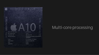
- 1. Multi-core processing Max. CPU clock rate to 2.34 GHz Min. feature size 14 nm Instruction set A64, A32, T32 Microarchitecture Hurricane and Zephyr both ARMv8-A- compatible Cores 2× Hurricane + 2× Zephyr Predecessor Apple A9, Apple A9X GPU 6-core Application Mobile
- 2. Review of multi-core processing based on By M-Reza Khalifeh Mahmoodi
- 3. Presentation name goes here Multi-core processing Microprocessor is an IC which has only the Central Processing Unit (CPU) They lack RAM, ROM, and other peripherals The Intel Pentium series, i3, i5, Cortex A8 are popular microprocessors which find their applications in desktop PC’s, Laptops, notepads etc. To deploy a microprocessor peripherals are required to be connected What is microcontroller and microprocessor ??? 03M-Reza Khalifeh Mahmoodi
- 4. Presentation name goes here Multi-core processing microcontrollers possess a CPU along with RAM, ROM, and other peripherals microcontrollers possess a CPU along with RAM, ROM, and other peripherals power is far less as compared to an actual computer Popular microcontrollers in the market are 8051, STM32, PIC32, Arduino, ATMEL etc. What is microcontroller and microprocessor ??? 04M-Reza Khalifeh Mahmoodi
- 5. Presentation name goes here microprocessor microcontroller 05 Multi-core processing Microprocessors are designed for generic and unspecific applications like on a PC. There is generally an Operating System (OS) installed which coordinates the different I/O’s. They need high amount of resources like RAM, ROM, I/O ports etc, which leads to increase in total cost of the system. Microcontrollers are designed to perform specific tasks. For example washing machine, refrigerator, microwave, cars, bikes, telephones etc. As the application is limited to one or two processes, they require small resources like RAM, ROM, I/O ports etc. This allows the integration of all these components on a single chip leading to reduced size and cost. M-Reza Khalifeh Mahmoodi
- 6. Presentation name goes here Multi-core processing 06 Attributes Microcontrollers Microprocessors Application Are application specific and are designed to perform certain limited tasks. Have generic application and are capable of executing big and complicated tasks. One Solution Have inbuilt processor, RAM, ROM and I/O Ports. Like a small stand-alone computer in a single Integrate Chip. Generally don’t have inbuilt RAM, ROM and I/O ports. The pins are used to interface with external RAM, ROM and ports. Performance Limited performance. Very high performance. Speed Generally operate at speeds from 8 MHz – 200 MHz. Generally operate at speeds above 1 GHz. Power Consumption Are embedded inside other devices, so are designed to consume less power. Consume relative more power. As performance is the given higher weightage over power. Cost Affordable and cheap. Can get started with a minimum external circuit. Very expensive and requires other peripherals to work along. M-Reza Khalifeh Mahmoodi
- 7. Presentation name goes here Altera Analog Devices Atmel Cypress Semiconductor Maxim Integrated ELAN Microelectronics Corp. EPSON Semiconductor Freescale Semiconductor Fujitsu Holtek Hyperstone Infineon Intel Lattice Semiconductor Microchip Technology National Semiconductor NEC 19 NXP Semiconductors Panasonic Rabbit Semiconductor Renesas Electronics Rockwell Silicon Laboratories Silicon Motion Sony Spansion STMicroelectronics Texas Instruments Toshiba Ubicom Xemics Xilinx XMOS ZiLOG This is a list of common microcontrollers listed by brand
- 8. Presentation name goes here ARM is the industry's leading supplier of microprocessor technology, offering the widest range of microprocessor cores to address the performance, power and cost requirements for almost all application markets. Combining a vibrant ecosystem with over 1,000 partners delivering silicon, development tools and software, and more than 86 billion processors sold, ARM truly is “The Architecture for the Digital World ARM, originally Acorn RISC Machine, later Advanced RISC Machine, is a family of reduced instruction set computing (RISC) architectures for computer processors, configured for various environments. British company ARM Holdings develops the architecture and licenses it to other companies In 2009, some manufacturers introduced netbooks based on ARM architecture CPUs, in direct competition with netbooks based on Intel Atom. According to analyst firm IHS iSuppli, by 2015, ARM Integrated circuits may be in 23% of all laptops. A RISC-based computer design approach means processors require fewer transistors than typical complex instruction set computing (CISC) x86 processors in most personal computers. This approach reduces costs, heat and power use. These characteristics are desirable for light, portable, battery-powered devices—including, smartphones, laptops and tablet computers, and other embedded systems. For supercomputers, which consume large amounts of electricity, ARM could also be a power-efficient solution ARM Holdings 08 Multi-core processing M-Reza Khalifeh Mahmoodi
- 9. Presentation name goes here 09 ARM family ARM architecture ARM core Feature Cache (I / D), MMU Typical MIPS @ MHz ARM1 ARMv1 ARM1 First implementation None ARM2 ARMv2 ARM2 ARMv2 added the MUL (multiply) instruction None 4 MIPS @ 8 MHz 0.33 DMIPS/MHz ARMv2a ARM250 Integrated MEMC (MMU ), graphics and I/O processor. ARMv2a added the SWP and SWPB (swap) instructions None, MEMC1a 7 MIPS @ 12 MHz ARM3 ARMv2a ARM3 First integrated memory cache 4 KB unified 12 MIPS @ 25 MHz 0.50 DMIPS/MHz ARM6 ARMv3 ARM60 ARMv3 first to support 32-bit memory address space (previously 26- bit). ARMv3M first added long multiple instructions (32x32=64). None 10 MIPS @ 12 MHz ARM600 As ARM60, cache and coprocessor bus (for FPA10 floating-point unit) 4 KB unified 28 MIPS @ 33 MHz ARM610 As ARM60, cache, no coprocessor bus 4 KB unified 17 MIPS @ 20 MHz 0.65 DMIPS/MHz ARM7 ARMv3 ARM700 8 KB unified 40 MHz ARM710 As ARM700, no coprocessor bus 8 KB unified 40 MHz ARM710a As ARM710 8 KB unified 40 MHz 0.68 DMIPS/MHz This is a list of microarchitectures based on the ARM family Multi-core processing M-Reza Khalifeh Mahmoodi
- 10. Presentation name goes here 10 ARM7T ARMv4T ARM7TDMI(-S) 3-stage pipeline, Thumb, ARMv4 first to drop legacy ARM 26- bit addressing None 15 MIPS @ 16.8 MHz 63 DMIPS @ 70 MHz ARM710T As ARM7TDMI, cache 8 KB unified, MMU 36 MIPS @ 40 MHz ARM720T As ARM7TDMI, cache 8 KB unified, MMU with FCSE (Fast Context Switch Extension) 60 MIPS @ 59.8 MHz ARM740T As ARM7TDMI, cache MPU ARM7EJ ARMv5TEJ ARM7EJ-S 5-stage pipeline, Thumb, Jazelle DBX, Enhanced DSP instructions None ARM8 ARMv4 ARM810[4][5] 5-stage pipeline, static branch prediction, double-bandwidth memory 8 KB unified, MMU 84 MIPS @ 72 MHz 1.16 DMIPS/MHz ARM9T ARMv4T ARM9TDMI 5-stage pipeline, Thumb None ARM920T As ARM9TDMI, cache 16 KB / 16 KB, MMU with FCSE (Fast Context Switch Extension)[6] 200 MIPS @ 180 MHz ARM922T As ARM9TDMI, caches 8 KB / 8 KB, MMU ARM940T As ARM9TDMI, caches 4 KB / 4 KB, MPU ARM9E ARMv5TE ARM946E-S Thumb, Enhanced DSP instructions, caches Variable, tightly coupled memories, MPU ARM966E-S Thumb, Enhanced DSP instructions No cache, TCMs ARM968E-S As ARM966E-S No cache, TCMs ARMv5TEJ ARM926EJ-S Thumb, Jazelle DBX, Enhanced DSP instructions Variable, TCMs, MMU 220 MIPS @ 200 MHz ARMv5TE ARM996HS Clockless processor, as ARM966E-S No caches, TCMs, MPU ARM family ARM architecture ARM core Feature Cache (I / D), MMU Typical MIPS @ MHz Multi-core processing M-Reza Khalifeh Mahmoodi
- 11. Presentation name goes here 11 ARM10E ARMv5TE ARM1022E As ARM1020E 16 KB / 16 KB, MMU ARMv5TEJ ARM1026EJ-S Thumb, Jazelle DBX, Enhanced DSP instructions, (VFP) Variable, MMU or MPU ARM11 ARMv6 ARM1136J(F)-S[7] 8-stage pipeline, SIMD, Thumb, Jazelle DBX, (VFP), Enhanced DSP instructions Variable, MMU 740 @ 532–665 MHz (i.MX31 SoC), 400– 528 MHz ARMv6T2 ARM1156T2(F)-S 9-stage pipeline,[8] SIMD, Thumb-2, (VFP), Enhanced DSP instructions Variable, MPU ARMv6Z ARM1176JZ(F)-S As ARM1136EJ(F)-S Variable, MMU + TrustZone 965 DMIPS @ 772 MHz, up to 2,600 DMIPS with four processors[9] ARMv6K ARM11MPCore As ARM1136EJ(F)-S, 1–4 core SMP Variable, MMU SecurCore ARMv6-M SC000 0.9 DMIPS/MHz ARMv4T SC100 ARMv7-M SC300 1.25 DMIPS/MHz Cortex-M ARMv6-M Cortex-M0[10] Microcontroller profile, most Thumb + some Thumb-2,[11] hardware multiply instruction (optional small), optional system timer, optional bit- banding memory Optional cache, no TCM, no MPU 0.84 DMIPS/MHz Cortex-M0+[12] Microcontroller profile, most Thumb + some Thumb-2,[11] hardware multiply instruction (optional small), optional system timer, optional bit- banding memory Optional cache, no TCM, optional MPU with 8 regions 0.93 DMIPS/MHz Cortex-M1[13] Microcontroller profile, most Thumb + some Thumb-2,[11] hardware multiply instruction (optional small), OS option adds SVC / banked stack pointer, optional system timer, no bit-banding memory Optional cache, 0-1024 KB I-TCM, 0- 1024 KB D-TCM, no MPU 136 DMIPS @ 170 MHz,[14](0.8 DMIPS/MHz FPGA- dependent)[15] ARMv7-M Cortex-M3[16] Microcontroller profile, Thumb / Thumb-2, hardware multiply and divide instructions, optional bit-banding memory Optional cache, no TCM, optional MPU with 8 regions 1.25 DMIPS/MHz ARMv7E-M Cortex-M4[17] Microcontroller profile, Thumb / Thumb-2 / DSP / optional VFPv4-SP single-precision FPU, hardware multiply and divide instructions, optional bit-banding memory Optional cache, no TCM, optional MPU with 8 regions 1.25 DMIPS/MHz (1.27 w/FPU) Cortex-M7[18] Microcontroller profile, Thumb / Thumb-2 / DSP / optional VFPv5 single and double precision FPU, hardware multiply and divide instructions 0-64 KB I-cache, 0-64 KB D-cache, 0-16 MB I-TCM, 0-16 MB D-TCM (all these w/optional ECC), optional MPU with 8 or 16 regions 2.14 DMIPS/MHz Multi-core processing M-Reza Khalifeh Mahmoodi
- 12. Presentation name goes here 12 Cortex-R ARMv7-R Cortex-R4[19] Real-time profile, Thumb / Thumb-2 / DSP / optional VFPv3 FPU, hardware multiply and optional divide instructions, optional parity & ECC for internal buses / cache / TCM, 8-stage pipeline dual-core running lockstep with fault logic 0–64 KB / 0–64 KB, 0–2 of 0–8 MB TCM, opt MPU with 8/12 regions Cortex-R5[20] Real-time profile, Thumb / Thumb-2 / DSP / optional VFPv3 FPU and precision, hardware multiply and optional divide instructions, optional parity & ECC for internal buses / cache / TCM, 8-stage pipeline dual-core running lock-step with fault logic / optional as 2 independent cores, low-latency peripheral port (LLPP), accelerator coherency port (ACP)[21] 0–64 KB / 0–64 KB, 0–2 of 0–8 MB TCM, opt MPU with 12/16 regions Cortex-R7[22] Real-time profile, Thumb / Thumb-2 / DSP / optional VFPv3 FPU and precision, hardware multiply and optional divide instructions, optional parity & ECC for internal buses / cache / TCM, 11-stage pipeline dual-core running lock-step with fault logic / out-of-order execution / dynamic register renaming / optional as 2 independent cores, low-latency peripheral port (LLPP), ACP[21] 0–64 KB / 0–64 KB, ? of 0–128 KB TCM, opt MPU with 16 regions Cortex-R8[23] TBD TBD Multi-core processing M-Reza Khalifeh Mahmoodi
- 13. Presentation name goes here 13 Cortex-A (32-bit) ARMv7-A Cortex-A5[24] Application profile, ARM / Thumb / Thumb-2 / DSP / SIMD / Optional VFPv4- D16 FPU / Optional NEON / Jazelle RCT and DBX, 1–4 cores / optional MPCore, snoop control unit (SCU), generic interrupt controller (GIC), accelerator coherence port (ACP) 4-64 KB / 4-64 KB L1, MMU + TrustZone 1.57 DMIPS/MHz per core Cortex-A7[25] Application profile, ARM / Thumb / Thumb-2 / DSP / VFPv4-D16 FPU / NEON / Jazelle RCT and DBX / Hardware virtualization, in-order execution, superscalar, 1–4 SMP cores, MPCore, Large Physical Address Extensions (LPAE), snoop control unit (SCU), generic interrupt controller (GIC), ACP, architecture and feature set are identical to A15, 8-10 stage pipeline, low-power design[26] 8-64 KB / 8-64 KB L1, 0–1 MB L2, MMU + TrustZone 1.9 DMIPS/MHz per core Cortex-A8[27] Application profile, ARM / Thumb / Thumb-2 / VFPv3 FPU / NEON / Jazelle RCT and DAC, 13-stage superscalar pipeline 16-32 KB / 16–32 KB L1, 0–1 MB L2 opt ECC, MMU + TrustZone Up to 2000 (2.0 DMIPS/MHz in speed from 600 MHz to greater than 1 GHz) Cortex-A9[28] Application profile, ARM / Thumb / Thumb-2 / DSP / Optional VFPv3 FPU / Optional NEON / Jazelle RCT and DBX, out-of-order speculative issue superscalar, 1–4 SMP cores, MPCore, snoop control unit (SCU), generic interrupt controller (GIC), accelerator coherence port (ACP) 16–64 KB / 16–64 KB L1, 0–8 MB L2 opt parity, MMU + TrustZone 2.5 DMIPS/MHz per core, 10,000 DMIPS @ 2 GHz on Performance Optimized TSMC 40G (dual-core) Cortex-A12[29] Application profile, ARM / Thumb-2 / DSP / VFPv4 FPU / NEON / Hardware virtualization, out-of-order speculative issue superscalar, 1–4 SMP cores, Large Physical Address Extensions (LPAE), snoop control unit (SCU), generic interrupt controller (GIC), accelerator coherence port (ACP) 32-64 KB 3.0 DMIPS/MHz per core Cortex-A15[30] Application profile, ARM / Thumb / Thumb-2 / DSP / VFPv4 FPU / NEON / integer divide / fused MAC / Jazelle RCT / hardware virtualization, out-of- order speculative issue superscalar, 1–4 SMP cores, MPCore, Large Physical Address Extensions (LPAE), snoop control unit (SCU), generic interrupt controller (GIC), ACP, 15-24 stage pipeline[26] 32 KB w/parity / 32 KB w/ECC L1, 0– 4 MB L2, L2 has ECC, MMU + TrustZone At least 3.5 DMIPS/MHz per core (up to 4.01 DMIPS/MHz depending on implementation)[31] Cortex-A17[32] Application profile, ARM / Thumb / Thumb-2 / DSP / VFPv4 FPU / NEON / integer divide / fused MAC / Jazelle RCT / hardware virtualization, out-of- order speculative issue superscalar, 1–4 SMP cores, MPCore, Large Physical Address Extensions (LPAE), snoop control unit (SCU), generic interrupt controller (GIC), ACP 32 KB L1, 256 KB-8 MB L2 w/optional ECC 2.8 DMIPS/MHz ARMv8-A Cortex-A32[33] Application profile, AArch32, 1-4 SMP cores, TrustZone, NEON advanced SIMD, VFPv4, hardware virtualization, dual issue, in-order pipeline 8-64 KB w/optional parity / 8-64 KB w/optional ECC L1 per core, 128 KB-1 MB L2 w/optional ECC shared Multi-core processing M-Reza Khalifeh Mahmoodi
- 14. Presentation name goes here 14 Cortex-A (64-bit) ARMv8-A Cortex-A35[34] Application profile, AArch32 and AArch64, 1-4 SMP cores, TrustZone, NEON advanced SIMD, VFPv4, hardware virtualization, dual issue, in- order pipeline 8-64 KB w/parity / 8-64 KB w/ECC L1 per core, 128 KB-1 MB L2 shared, 40-bit physical addresses 1.78 DMIPS/MHz Cortex-A53[35] Application profile, AArch32 and AArch64, 1-4 SMP cores, TrustZone, NEON advanced SIMD, VFPv4, hardware virtualization, dual issue, in-order pipeline 8-64 KB w/parity / 8-64 KB w/ECC L1 per core, 128 KB-2 MB L2 shared, 40- bit physical addresses 2.3 DMIPS/MHz Cortex-A57[36] Application profile, AArch32 and AArch64, 1-4 SMP cores, TrustZone, NEON advanced SIMD, VFPv4, hardware virtualization, multi-issue, deeply out-of- order pipeline 48 KB w/DED parity / 32 KB w/ECC L1 per core; 512 KB-2 MB L2 shared w/ECC; 44-bit physical addresses 4.6 DMIPS/MHz Cortex-A72[37] Application profile, AArch32 and AArch64, 1-4 SMP cores, TrustZone, NEON advanced SIMD, VFPv4, hardware virtualization, multi-issue, deeply out-of- order pipeline 48 KB w/DED parity / 32 KB w/ECC L1 per core; 512 KB-2 MB L2 shared w/ECC; 44-bit physical addresses 4.8 DMIPS/MHz Cortex-A73[38] Application profile, AArch32 and AArch64, 1-4 SMP cores, TrustZone, NEON advanced SIMD, VFPv4, hardware virtualization, multi-issue, deeply out-of- order pipeline 64 KB / 32-64 KB L1 per core, 256 KB-8 MB L2 shared w/ optional ECC, 44- bit physical addresses 4.9 DMIPS/MHz M-Reza Khalifeh Mahmoodi Multi-core processing
- 15. Presentation name goes here Why should we use Multi-core processing instead of Single-core ?Mobile devices perform a wide variety of tasks such as Web browsing, video playback, mobile gaming, SMS text messaging, and location-based services. Due to the growth in the availability of high speed mobile and Wi-Fi networks, mobile devices will also be used for various performance-intensive tasks that were previously handled by traditional PCs. The next generation of smartphones (called “Super phones”) and tablets will be used for a wide variety of tasks such as playback of high definition 1080p videos, Adobe® Flash®-based online gaming, Flash-based streaming high definition videos, visually rich gaming, video editing, simultaneous HD video downloads, encode and uploads, and real-time HD video conferencing. 15
- 16. Presentation name goes here Difficult to make single-core clock frequencies even higher P = C × V 2 × F Moore's law Deeply pipelined circuits: heat problems speed of light problems difficult design and verification large design teams necessary server farms need expensive air-conditioning Many new applications are multithreaded Why should we use Multi- core processing instead Single-core ? The Unique Screen Mockup 16 Multi-core processing M-Reza Khalifeh Mahmoodi
- 17. Presentation name goes here Multi-core processing Large problems can often be divided into smaller ones Several different forms of parallel computing Bit-level - processor word size Instruction-level – Hardware & Software e = a + b f = c + d m = e * f Task parallelism Data Parallel computing ??? 17M-Reza Khalifeh Mahmoodi
- 18. Presentation name goes here Multi-core processing speedup from parallelization would be linear doubling the number of processing elements should halve the runtime Slatency (s) = 1 1−𝑃+ 𝑃 𝑆 Slatency is the potential speedup in latency of the whole task; s is the speedup in latency of the execution of the parallelizable part of the task; P is the percentage of the execution time of the whole task concerning the parallelizable part of the task before parallelization.Speedup in a serial program Speedup in a serial program For example, with a serial program in two parts A and B for which TA = 3 s and TB = 1 s, Amdahl's law ? 18M-Reza Khalifeh Mahmoodi
- 19. Presentation name goes here Michael J. Flynn Flynn proposed Flynn's taxonomy, a method of classifying digital computers, in 1966 professor emeritus at Stanford University Flynn's taxonomy !!!! Classifications Single instruction stream single data stream (SISD) Single instruction stream, multiple data streams (SIMD) Multiple instruction streams, single data stream (MISD) Multiple instruction streams, multiple data streams (MIMD) Further divisions Single program, multiple data streams (SPMD) Multiple programs, multiple data streams (MPMD) 19 Multi-core processing M-Reza Khalifeh Mahmoodi
- 20. Presentation name goes here Developers must also choose the appropriate form of multiprocessing for their application requirements. This choice will determine how easily both new and existing code can achieve maximum concurrency. As Table 1 illustrates, developers have three basic forms to choose from: Asymmetric multiprocessing (AMP), Symmetric multiprocessing (SMP) Bound multiprocessing (BMP). Running AMP, SMP or BMP Mode for Multicore Systems 20 Model How it Works Key Advantages Asymmetric multiprocessi ng (AMP) A separate OS, or a separate copy of the same OS, manages each core. Typically, each software process is locked to a single core (e.g. process A runs only on core 1, process B runs only on core 2, etc.). Provides an execution environment similar to that of uniprocessor systems, allowing simple migration of legacy code. Also allows developers to manage each core independently. Symmetric multiprocessi ng (SMP) A single OS manages all processor cores simultaneously. The OS can dynamically schedule any process on any core, enabling full utilization of all cores. Provides greater scalability and parallelism than AMP, along with simpler shared resource management. Bound multiprocessi ng (BMP) A single OS manages all cores simultaneously. As in SMP, the OS can dynamically schedule processes on any core. However, the developer can also lock any process (and all of its associated threads) to a specific core. Combines the developer control of AMP with the transparent resource management of SMP. The option to lock threads to any core simplifies migration of legacy code and allows designers to dedicate cores Multi-core processing M-Reza Khalifeh Mahmoodi
- 21. Presentation name goes here Multi-core processing process and all of its threads are locked to a single processor core CPU Utilization in AMP Mode 21M-Reza Khalifeh Mahmoodi
- 22. Presentation name goes here Multi-core processing SMP addresses many of the issues by running only one copy of an OS across all the chip’s cores. Because the OS has insight into all system elements at all times, it can allocate resources on multiple cores with little or no input from the application designer Symmetric Multiprocessing (SMP) Mode 22M-Reza Khalifeh Mahmoodi
- 23. Presentation name goes here An introduction to NXP NXP Semiconductors N.V. is a Dutch global semiconductor manufacturer headquartered in Eindhoven, Netherlands. The company employs approximately 45,000 people in more than 35 countries, including 11,200 engineers in 23 countries. NXP reported revenue of $6.1 billion in 2015, including one month of revenue contribution from recently merged Freescale Semiconductor. NXP said it was the fifth-largest non-memory semiconductor supplier in 2016, NXP is the co-inventor of near field communication (NFC) technology NXP manufactures automotive chips for in-vehicle networking NXP invented the I²C interface over 30 years ago 23 Multi-core processing M-Reza Khalifeh Mahmoodi
- 24. Presentation name goes here An example of ‘Single-core’ ARM Architecture 24 NXP, microcontroller based on a CORTEX-M3 , ARM family and the best technical example of this family is LPC178x/7x series and more specifically LPC1788 Microcontroller. ARMv7-M , Microcontroller profile, Thumb / Thumb-2, hardware multiply and divide instructions, optional bit-banding memory 32-bit ARM Cortex-M3 microcontroller; up to 512 kB flash and 96 kB SRAM; USB Device/Host/OTG; Ethernet; LCD; EMC The LPC178x/7x adds a specialized flash memory accelerator to accomplish optimal performance when executing code from flash. The LPC178x/7x operates at up to 120 MHz CPU frequency. Multi-core processing M-Reza Khalifeh Mahmoodi
- 25. Presentation name goes here An example of ‘Single-core’ ARM Architecture 25 Multi-core processing M-Reza Khalifeh Mahmoodi
- 26. Presentation name goes here Multiprocessor System Designs come with a number of challenges 26 Multiprocessor System Designs is the need for low power capability the higher total memory system and bus bandwidth is required careful bus architecture planning is needed Multi-core processing M-Reza Khalifeh Mahmoodi
- 27. Presentation name goes here 26M-Reza Khalifeh Mahmoodi TMS 1000 8,000 1974 Texas Instruments 8,000 nm Intel 4004 2,300 1971 Intel 10,000 nm 12 mm² Intel 8008 3,500 1972 Intel 10,000 nm 14 mm² Intel 8086 29,000 1978 Intel 3,000 nm 33 mm² Intel 8088 29,000 1979 Intel 3,000 nm 33 mm² Intel 80386 275,000 1985 Intel 1,500 nm 104 mm² ARM 1 25,000[7] 1985 Acorn 3,000 nm 50 mm² Intel 80486 1,180,235 1989 Intel 1000 nm 173 mm² ARM 3 300,000 1989 Acorn ARM 6 35,000 1991 ARM Pentium 3,100,000 1993 Intel 800 nm 294 mm² ARM 9TDMI 111,000 1999 Acorn 350 nm 4.8 mm² Pentium Pro 5,500,000 1995 Intel 500 nm 307 mm² Core 2 Duo Conroe 291,000,000 2006 Intel 65 nm 143 mm² Core 2 Duo Allendale 169,000,000 2007 Intel 65 nm 111 mm² Itanium 2 Madison 6M 410,000,000 2003 Intel 130 nm 374 mm² ARM Cortex-A9 26,000,000 2007 ARM 45 nm 31 mm² Core 2 Duo Wolfdale 3M 230,000,000 2008 Intel 45 nm 83 mm² Itanium 2 with 9 MB cache 592,000,000 2004 Intel 130 nm 432 mm² Core i7 (Quad) 731,000,000 2008 Intel 45 nm 263 mm² Apple A7 (dual- core ARM64 "mobile SoC") 1,000,000,000 2013 Apple 28 nm 102 mm² 22-core Xeon Broadwell-E5 7,200,000,000 2016 Intel 14 nm 456 mm² SPARC M7 10,000,000,000 2015 Oracle 20 nm GP100 Pascal 15,300,000,000 2016 Nvidia 16 nm 610 mm² Challenges for low power capability
- 28. Presentation name goes here 28M-Reza Khalifeh Mahmoodi Challenges for low power capability Simplest way: Core standby mode algorithm
- 29. Presentation name goes here Challenges for bus bandwidth 29 Simple dual core system with ROM sharing gets 78% of ideal performance in Dhrystone 2.1 Verilog simulation using of a 64-bit flash and simple fetch buffer 92% Multi-core processing M-Reza Khalifeh Mahmoodi
- 30. Presentation name goes here LPC microcontrollers based on ARM Cortex-M4 Core (single- and multi-core) LPC43XX series 24 Cortex-M4 or M4F cores up to 204 MHz Highest performance, best power efficiency DSP options, multi-high-speed connectivity, advanced peripherals Cortex-M0+ or M0 coprocessors Multi-core processing M-Reza Khalifeh Mahmoodi
- 31. Presentation name goes here LPC4350: 31 Multi-core processing M-Reza Khalifeh Mahmoodi 32-bit ARM Cortex-M4/M0 MCU; up to 264 kB SRAM; Ethernet; two High-speed USBs; advanced configurable peripherals
- 32. Presentation name goes here i.MX 8 Family processors based on ARM® Cortex-A53, Cortex-A72 + Cortex-M4 cores 32 Multi-core processing M-Reza Khalifeh Mahmoodi Multi-screen (4x) support Fast multi-OS platform deployment via advanced full-chip hardware virtualization and domain protection Deploy rich, fully-independent graphics content across 4x HD screens or 1x 4K screen Android™*, Linux®*, FreeRTOS, QNX™*, Green Hills®, Dornerworks* XEN™* Automotive AEC-Q100 Grade 3 (-40° to 125° C Tj), Industrial (-40° to 105° C Tj), Consumer (-20° to 105° C Tj) Fully supported on NXP’s 10 and 15-year Longevity Program
- 33. Presentation name goes here http://theembeddedguy.com/2016/05/09/microcontroller-vs-microprocessor/ https://en.wikipedia.org/wiki/List_of_common_microcontrollers https://en.wikipedia.org/wiki/List_of_ARM_microarchitectures https://www.eeweb.com/blog/arm/multi-core-mcu-design-with-arm-cortex-m- processors-and-coresight-soc http://www.nxp.com/products/microcontrollers-and-processors/arm-processors/lpc- cortex-m-mcus:LPC-ARM-CORTEX-M-MCUS http://www.nxp.com/ http://www.intel.eu/ http://www.st.com/ http://www.ti.com/ References: 08 Multi-core processing M-Reza Khalifeh Mahmoodi