Top 10 Most Downloaded Games on Play Store in 2024
Lecture 19
1. Basic Computer Orgsnization and Design 1 Lecture 19
CSE 211, Computer Organization and Architecture Harjeet Kaur, CSE/IT
Overview
Instruction Codes
Computer Registers
Computer Instructions
Timing and Control
Instruction Cycle
Memory Reference Instructions
Input-Output and Interrupt
Complete Computer Description
2. Basic Computer Orgsnization and Design 2 Lecture 19
CSE 211, Computer Organization and Architecture Harjeet Kaur, CSE/IT
Complete Computer Design
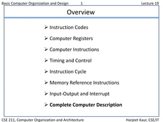
=1 (I/O) =0 (Register) =1(Indir) =0(Dir)
start
SC 0, IEN 0, R 0
R
AR PC
R’T0
IR M[AR], PC PC + 1
R’T1
AR IR(0~11), I IR(15)
D0...D7 Decode IR(12 ~ 14)
R’T2
AR 0, TR PC
RT0
M[AR] TR, PC 0
RT1
PC PC + 1, IEN 0
R 0, SC 0
RT2
D7
I I
Execute
I/O
Instruction
Execute
RR
Instruction
AR <- M[AR] Idle
D7IT3 D7I’T3 D7’IT3 D7’I’T3
Execute MR
Instruction
=0(Instruction =1(Interrupt
Cycle) Cycle)
=1(Register or I/O) =0(Memory Ref)
D7’T4
3. Basic Computer Orgsnization and Design 3 Lecture 19
CSE 211, Computer Organization and Architecture Harjeet Kaur, CSE/IT
Complete Computer Design
Fetch
Decode
Indirect
Interrupt
Memory-Reference
AND
ADD
LDA
STA
BUN
BSA
ISZ
RT0:
RT1:
RT2:
D7IT3:
RT0:
RT1:
RT2:
D0T4:
D0T5:
D1T4:
D1T5:
D2T4:
D2T5:
D3T4:
D4T4:
D5T4:
D5T5:
D6T4:
D6T5:
D6T6:
AR PC
IR M[AR], PC PC + 1
D0, ..., D7 Decode IR(12 ~ 14),
AR IR(0 ~ 11), I IR(15)
AR M[AR]
R 1
AR 0, TR PC
M[AR] TR, PC 0
PC PC + 1, IEN 0, R 0, SC 0
DR M[AR]
AC AC DR, SC 0
DR M[AR]
AC AC + DR, E Cout, SC 0
DR M[AR]
AC DR, SC 0
M[AR] AC, SC 0
PC AR, SC 0
M[AR] PC, AR AR + 1
PC AR, SC 0
DR M[AR]
DR DR + 1
M[AR] DR, if(DR=0) then (PC PC + 1),
SC 0
4. Basic Computer Orgsnization and Design 4 Lecture 19
CSE 211, Computer Organization and Architecture Harjeet Kaur, CSE/IT
Complete Computer Design
Register-Reference
CLA
CLE
CMA
CME
CIR
CIL
INC
SPA
SNA
SZA
SZE
HLT
Input-Output
INP
OUT
SKI
SKO
ION
IOF
D7IT3 = r
IR(i) = Bi
r:
rB11:
rB10:
rB9:
rB8:
rB7:
rB6:
rB5:
rB4:
rB3:
rB2:
rB1:
rB0:
D7IT3 = p
IR(i) = Bi
p:
pB11:
pB10:
pB9:
pB8:
pB7:
pB6:
(Common to all register-reference instr)
(i = 0,1,2, ..., 11)
SC 0
AC 0
E 0
AC AC
E E
AC shr AC, AC(15) E, E AC(0)
AC shl AC, AC(0) E, E AC(15)
AC AC + 1
If(AC(15) =0) then (PC PC + 1)
If(AC(15) =1) then (PC PC + 1)
If(AC = 0) then (PC PC + 1)
If(E=0) then (PC PC + 1)
S 0
(Common to all input-output instructions)
(i = 6,7,8,9,10,11)
SC 0
AC(0-7) INPR, FGI 0
OUTR AC(0-7), FGO 0
If(FGI=1) then (PC PC + 1)
If(FGO=1) then (PC PC + 1)
IEN 1
IEN 0
5. Basic Computer Orgsnization and Design 5 Lecture 19
CSE 211, Computer Organization and Architecture Harjeet Kaur, CSE/IT
Design of a Basic Computer(BC)
Hardware Components of BC
A memory unit: 4096 x 16.
Registers:
AR, PC, DR, AC, IR, TR, OUTR, INPR, and SC
Flip-Flops(Status):
I, S, E, R, IEN, FGI, and FGO
Decoders: a 3x8 Opcode decoder
a 4x16 timing decoder
Common bus: 16 bits
Control logic gates:
Adder and Logic circuit: Connected to AC
Control Logic Gates
- Input Controls of the nine registers
- Read and Write Controls of memory
- Set, Clear, or Complement Controls of the flip-flops
- S2, S1, S0 Controls to select a register for the bus
- AC, and Adder and Logic circuit
![Basic Computer Orgsnization and Design 2 Lecture 19
CSE 211, Computer Organization and Architecture Harjeet Kaur, CSE/IT
Complete Computer Design
=1 (I/O) =0 (Register) =1(Indir) =0(Dir)
start
SC 0, IEN 0, R 0
R
AR PC
R’T0
IR M[AR], PC PC + 1
R’T1
AR IR(0~11), I IR(15)
D0...D7 Decode IR(12 ~ 14)
R’T2
AR 0, TR PC
RT0
M[AR] TR, PC 0
RT1
PC PC + 1, IEN 0
R 0, SC 0
RT2
D7
I I
Execute
I/O
Instruction
Execute
RR
Instruction
AR <- M[AR] Idle
D7IT3 D7I’T3 D7’IT3 D7’I’T3
Execute MR
Instruction
=0(Instruction =1(Interrupt
Cycle) Cycle)
=1(Register or I/O) =0(Memory Ref)
D7’T4](data:image/gif;base64,R0lGODlhAQABAIAAAAAAAP///yH5BAEAAAAALAAAAAABAAEAAAIBRAA7)