1. 1. What are tri-state devices and why they are essential in a bus oriented system?
Electronic logic uses just two states, high and low voltage, or "1" and "0". The output of a
gate will always be at one value or the other. This is convenient when only a single output is used
to drive a signal. In some cases, it is useful to have two or more outputs driving the same signal
line. However, if two outputs are linked together, if they have different outputs, there is likely to be
damage to the outputs and the level on the line will be un-predictable. A tri-state output has the
same high and low levels as standard logic outputs but it has third state, namely high impedance
(Z). A high impedance state means that the output is not transferred to the line so effectively; the
output is simply turned off. Another logic gate can now drive the line and the level is entirely
predictable. Numerous outputs can now drive a single line as long as only on is turned on at any
time.
A device which has one input, one enable and one output line is called tri-state device, if two
different devices wants a common bus then tri-state device are essential to assign bus to any one
of them in bus orientation system.
In a multiplexed bus system, many devices are connected to a common bus. If 2 or more devices
attempt to use the bus at the same time, then data will be lost. Thus only one device must be
allowed to use the bus at a time. One method is to connect the devices through tri-state Devices,
which when disabled will effectively disconnect devices from the bus.
2. Explain priority encoder
The Priority Encoder is another type of combinational circuit similar to a binary encoder, except
that it generates an output code based on the highest prioritized input. Priority encoders are used
extensively in digital and computer systems as microprocessor interrupt controllers where they
detect the highest priority input.
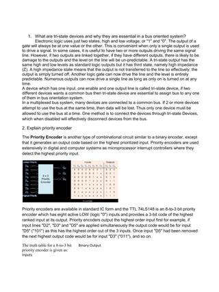
Priority encoders are available in standard IC form and the TTL 74LS148 is an 8-to-3 bit priority
encoder which has eight active LOW (logic "0") inputs and provides a 3-bit code of the highest
ranked input at its output. Priority encoders output the highest order input first for example, if
input lines "D2", "D3" and "D5" are applied simultaneously the output code would be for input
"D5" ("101") as this has the highest order out of the 3 inputs. Once input "D5" had been removed
the next highest output code would be for input "D3" ("011"), and so on.
The truth table for a 8-to-3 bit Binary Output
priority encoder is given as:
Inputs
2. D7 D6 D5 D4 D3 D2 D1 D0 Q2 Q1 Q0
0 0 0 0 0 0 0 1 0 0 0
0 0 0 0 0 0 1 X 0 0 1
0 0 0 0 0 1 X X 0 1 0
0 0 0 0 1 X X X 0 1 1
0 0 0 1 X X X X 1 0 0
0 0 1 X X X X X 1 0 1
0 1 X X X X X X 1 1 0
1 X X X X X X X 1 1 1
Then the final Boolean expression for the priority encoder including the zero inputs is defined as:
3. Differentiate between static RAM and dynamic RAM
STATIC RAM DYNAMIC RAM
1.Static ram use a number of transistor to 1. Dynamic ram use storage cell made of
store single bit. transistor and and capacitor.
2. SRAM store data till power of the computer 2. DRAM refreshed there data every
is switched on instance of time and retain the data for
a very short span of time, even after
the power is off
3. Static Ram is very costly 3. Dynamic Ram is cheaper.
4. Static Ram is faster the Dynamic Ram 4. while dynamic ram is slower then static
5. Static Ram is used in L1 and L2 cache.
5. Dynamic Ram is used in system RAM
4. Describe the operation of octal to binary encoder
Octal-to-Binary take 8 inputs and provides 3 outputs, thus doing the opposite of what the 3-to-8 decoder
does. At any one time, only one input line has a value of 1. The figure below shows the truth table of an
Octal-to-binary encoder.
3. TRUTH TABLE
I0 I1 I2 I3 I4 I5 I6 I7 Y2 Y1 Y0
1 0 0 0 0 0 0 0 0 0 0
0 1 0 0 0 0 0 0 0 0 1
0 0 1 0 0 0 0 0 0 1 0
0 0 0 1 0 0 0 0 0 1 1
0 0 0 0 1 0 0 0 1 0 0
0 0 0 0 0 1 0 0 1 0 1
0 0 0 0 0 0 1 0 1 1 0
0 0 0 0 0 0 0 1 1 1 1
For an 8-to-3 binary encoder with inputs I0-I7 the logic expressions of the outputs Y0-Y2 are:
Y1= I2 + I3 + I6 + I7
Y0 = I1 + I3 + I5 + I7
Y2 = I4 + I5 + I6 +I7 CRICUIT
5.Differentiate between RAM and ROM memories.
RAM ROM
1. RAM is Random Access Memory. 1. ROM is Read Only Memory
2. RAM is the memory available for the operating 2. ROM is the memory that comes with your
system, programs and processes to use when computer that is pre-written to hold the
the computer is running instructions for booting-up the computer
3. RAM requires a flow of electricity to retain data 3. ROM will retain data without the flow of
4. RAM is a type of volatile memory electricity
5. There are different types of RAM, including 4. ROM is a type of non- volatile memory
DRAM (Dynamic Random Access Memory) and 5. There are different types of ROM, including
SRAM (Static Random Access Memory). PROM (programmable read-only memory) that
is manufactured as blank memory (e.g. a CD-
ROM) and EPROM (erasable programmable
read-only memory).
6. What is a tri-state buffer? Why we need it?
An inverter is called a NOT gate, and it looks like:
4. The inverter is a triangle, followed by a circle/bubble. That circle sometimes appears by itself, and
means negation
The buffer is logic circuit that applies the current or power. It has one input line and one output
line. The logic output of the buffer is same as its input. A tri-state buffer is a device that allows you
to control when an output signal makes it to the bus. When the tri-state buffer's control bit is
active, the input of the device makes it to the output. This is when the "valve" is open. When it's
not active, the output of the device is Z, which is high-impedance or, equivalently, nothing. This is
when the "valve" is closed, and no electrical signal is allowed to pass to the outputA tri-state
buffer is a useful device that allows us to control when current passes through the device, and
when it doesn't. A tri-state buffer has two inputs: a data input x and a control input c. The control
input acts like a valve. When the control input is active, the output is the input. That is, it behaves
just like a normal buffer. The "valve" is closed. When the control input is not active, the output is
"Z". The "valve" is open, and no electrical current flows through. Thus, even if x is 0 or 1, that
value does not flow
7. Describe operation of 4:2 priority encoders
A 4-bit priority encoder (also sometimes called a priority decoder). This circuit basically converts
the 4-bit input into a binary representation. If the input n is active, all lower inputs (n-1 .. 0) are
ignored:
x3 x2 x1 x0 y1 y0
1 X X X 1 1
0 1 X X 1 0
0 0 1 X 0 1
0 0 0 X 0 0
The circuit operation is simple. Each output is driven by an OR-gate which is connected to the
NAND-INV outputs of the corresponding input lines. The NAND gate of each stage receives its
input bit, as well as the NAND gate outputs of all higher priority stages. This structure implies that
an active input on stage n effectively disables all lower stages n-1.. 0.
5. 8. Give classification of memories.
Memrory is divided into 2 patrs
1.RAM
2.ROM
1.ROM: This type of memory holds information permanently written on it. Usually it is called
non-volatile memory because it retains the information when the power is turned off. This
is an important feature of Read Only Memory. ROM is used to store computer startup
instructions. The instruction is pre-programmed by the manufacturer; means you can’t
modify or write back on ROM. Rom is divide into 3 parts
PROM (Programmable read-only memory)
EPROM (Erasable programmable read-only memory)
EEPROM(Electrically Erasable programmable read-only memory)
2.RAM: This is a type of memory serves as main memory of a computer. It temporarily
stores copy of information and files loaded from a computer hard drive that are required by
a processor. After finishing the modification or change you made on the loaded file, it must
be saved back to the hard drive before the power is turned off. If power is switched off
without saving, you won’t retrieve the change made on the original file.RAM IS DIVIDED
INTO 2 Parts
1. SRAM: .Static ram use a number of transistor to store single bit.
SRAM store data till power of the computer is switched on
Static Ram is very costly
Static Ram is faster the Dynamic Ram
DRAM: Dynamic ram use storage cell made of transistor and and capacitor.
DRAM refreshed there data every instance of time and retain the data for a very short
span of time, even after the power is off
Dynamic Ram is cheaper.
while dynamic ram is slower then static
6. 9.What is a latch? Describe its functions?
Latch – a memory element that does not have a clock input. State changes occur
in
response to a change in data input. Latches are commonly used in asynchronous
sequential switching circuits
10. What is a decoder? Explain the working of a decoder
A decoder is a combinational logic circuit that converts the binary code data at its input into one of a
number of different output lines one at a time producing an equivalent decimal code at its output
Binary Decoders: have inputs of 2-bit, 3-bit or 4-bit codes depending upon the number of data input
lines, and a n-bit decoder has 2n output lines. Therefore, if it receives n inputs (usually grouped as a
binary or Boolean number) it activates one and only one of its 2n outputs based on that input with all
other outputs deactivated. A decoder’s output code normally has more bits than its input code and
practical binary decoder circuits include 2-to-4, 3-to-8 and 4-to-16 line configurations. A binary
decoder converts coded inputs into coded outputs, where the input and output codes are different
and decoders are available to "decode" either a Binary or BCD (8421 code) input pattern to typically a
Decimal output code. Commonly available BCD-to-Decimal decoders include the TTL 7442 or the
CMOS 4028. An example of a 2-to-4 line decoder along with its truth table is given below. It consists
of an array of four NAND gates, one of which is selected for each combination of the input signals A
and B.
Memory Address Decoder: Binary Decoders are most often used in more complex digital systems to
access a particular memory location based on an "address" produced by a computing device. In
modern microprocessor systems the amount of memory required can be quite high and is generally
more than one single memory chip alone. One method of overcoming this problem is to connect lots
of individual memory chips together and to read the data on a common "Data Bus". In order to
prevent the data being "read" from each memory chip at the same time, each memory chip is
selected individually one at time and this process is known as Address Decoding. In this application,
the address represents the coded data input, and the outputs are the particular memory element select
signals. Each memory chip has an input called Chip Select or CS which is used by the MPU to select the
appropriate memory chip and a logic "1" on this input selects the device and a logic "0" on the input de-
selects it. By selecting or de-selecting each chip, allows us to select the correct memory device for a
particular address and when we specify a particular memory address, the corresponding memory location
exists ONLY in one of the chips