SlideShare une entreprise Scribd logo
1  sur  21
I. NIGHTLIGHT ANALOG AND
DIGITAL CIRCUIT
Fig.1 Nightlight analog circuit Fig.2 Nightlight digital circuit
By Wagner Nunes
A. Light Depended Resistor (LDR)
Fig. 3 Example of LDR component
Fig. 4 Example of the LDR function
in the exponential decay graphic
Fig. 7 Example of an LDR when resistance
increases
Fig. 6 Example of an LDR when resistance
decreases
Fig.5 Example of the electrons in
the valence band jumping to the
conduction band
• The LDR is made of a semiconductor
material that is layered on an
insulating material such as ceramic.
B. The Comparator
• 1) The Logic:
– If (V-) > (V+) => Vout ≈ GND or “0” low (-saturation)
– If (V+) < (V-) => Vout ≈ +Vcc or “1” high (+saturation)
Fig. 8 Example of a comparator output “0” Fig. 9 Example of a comparator output “1”
C. Function of the NPN Bipolar Junction
Transistor (BJT) as a Switch
• NPN (N stands for negative charge and P
stands for positive charge or hole)
• BJT(bipolar junction transistor ) is because it
involves both of these types of charger.
Fig. 11 Example of a transistor tuning the LED onFig. 10 the three regions of a NPN transistor
1) Cut - Off Region Conditions :
• Input base current IB= 0
• VBE < 0.7v
• Output collector current IC= 0
• Base – Collector junction BC is reversed biased
• Base – Emitter junction BE is reversed biased
• Maximum collector VCE= VCC
Fig. 12 Example of cut - off region conditions
1) Saturation Region Conditions
• Input base current (IB) connected to VCC
• VBE > 0.7v
• Max collector current IC= VCC/RC
• Base – Collector junction BC is forward biased
• Base – Emitter junction BE is forward biased
• VCE= 0 (ideal saturation)
Fig. 13 Example of saturation region conditions
Calculation for the collector resistor ( ) , base
current ( ) , and base resistor( )
IC = 20mA(datasheet)
VCE (Sat ) = 0.2V(datasheet)
bDC (direct current gain) = 60(datasheet)
IC = bDc ´ IB
-VCC + IC RC +VLED +VCE(Sat) = 0
-6V + 20mA ´ RC + 3.4V + 0.2V = 0
-2.4V + 20mA ´ RC = 0
RC =
2.4V
20mA
=120W
IB =
IC
bDC
= 333mA
RB =
6V - 0.7V
333mA
=16KW
IB
RB
RC
D. LED (light emitting diode)
Fig. 12 Example of the barrier potential
Fig. 14 Example of current in forward direction
on a diode
Fig. 15 Energy released by the
electron of a single photon.
Fig.13 An LED will begin to emit light when the
on-voltage is exceeded.
Fig. 11 Example of a blue 5mm LED
Calculation for energy released by the
electron of a single photon.
h (Plank 's constant) = 6.626 ´10-34
J / s
C(Coulomb) = 6. 25´1018
e-
c (Speed of light) = 3´108
m / s
l (called lambda or wavelength)
u ( frequency)
eV (electron volts)
lu = c
u =
c
l
=
3´108
m / s
470 ´10-9
m
= 640 ´1012
s-1
E( photon) = hu = (6. 626 ´10-34
J / s)´ (640 ´1012
s-1
) = 423´110-21
J
E(eV ) = E( photon) ´1Coulomb = (423´10-21
J)´ (6.25´1018
e-
) = 2. 6eV
Analog Circuit Schematic
II. NIGHTLIGHT DIGITAL CIRCUIT VERSION –
BASIC OPERATION
• Arduino Function:
– There is no analog output on Arduino. Instead it is a
digital output (on or off).
– If the output is half of the time on and half of the time
off, it is said to be 50% duty cycle.
– Duty cycle is the percentage of time that the output is
on. The output can be 30%, 20%, 10% duty cycle, or
any percentage from 0 – 100%.
– The Arduino has a technic called pulse width
modulation (PMW) that makes its output work as
analog.
Arduino Function:
• In the nightlight device, it allows the LED to fade
in and out going from 0 to 255 (8 bits = as a
default resolution) value repeating in a loop.
• 0 correspond to 0 volts and 255 to 5 volts and any
value in between are proportional to those
voltages.
• Then theses values are sent to the PWM pin
(PWM Pins 3, 5, 6, 9, 10, 11) thus fading the LED
in and out.
28
Arduino
Function – Pulse Width Modulation
Fig.18 Example of pulse width modulation
1) Formula for Duty Cycle:
DutyCycle=
TH
T
´100%
Voltage per step
(analogWrite( )) :
x=0 ® 255
xsteps
how many volts
xsteps
= x steps
5V
255 steps
=19.6mV per step
how many volts= x
5V
255
æ
è
ç
ö
ø
÷ =
E. Arduino
Function:
• This “function call” passes the read value
(argument) from the inputs (A0 to A5) to the
function in the library and its return an
integer, which is from 0 to 1023 (10 bits = )
as a default resolution).
• 0 corresponds to 0V and 1023 to 5V.
210
formula to calculate the voltages per
step on the input read
x = 0 ®1023
xsteps
how many volts
xsteps
= x steps
5V
1024 steps
= 4.88mV per step
how many volts= x
5V
1024
æ
è
ç
ö
ø
÷ =
Appendix C
Flowchart for the Digital Circuit
III. NIGHTLIGHT ANALOG CIRCUIT VERSION VS.
NIGHTLIGHT DIGITAL CIRCUIT VERSION
NIGHTLIGHT ANALOG CIRCUIT VERSION NIGHTLIGHT DIGITAL CIRCUIT VERSION
I spent more time with the digital circuit
than the analog one because of my
familiarity with it.
I improved my lack of skills with Arduino
the analog circuit required more space on
the board than the digital one due to
more parts used.
V. COST TO BUILD AND OPERATE
NIGHTLIGHT ANALOG CIRCUIT NIGHTLIGHT DIGITAL CIRCUIT
costs about $5.70 costs about $26.38, approximately five
times more (because of the Arduino )
+ Arduino can be used for other
applications because it is programmable.
Running on 6V (Maui Electric Company), 8
hours per day, the cost is $1.20 per
month.
Running on 6V battery, 8 hours per day,
the cost is $11 per month.
Conclusion
• As a result, this project spiked my interest
even more in electronics hardware, software,
and more about technology in general.
Consequently, after my associate degree in
the ECET, my next academic goal is to earn a
bachelor’s degree, become an electronic
computer engineer, and perhaps to earn a
master degree so I can teach electronics at a
university.
ETRO_296_Final_Presentation

Contenu connexe

Tendances

RF Circuit Design - [Ch3-2] Power Waves and Power-Gain Expressions
RF Circuit Design - [Ch3-2] Power Waves and Power-Gain ExpressionsRF Circuit Design - [Ch3-2] Power Waves and Power-Gain Expressions
RF Circuit Design - [Ch3-2] Power Waves and Power-Gain ExpressionsSimen Li
 
Temple, San Jose Interconnection App Stamped (1)
Temple, San Jose Interconnection App Stamped (1)Temple, San Jose Interconnection App Stamped (1)
Temple, San Jose Interconnection App Stamped (1)John Turner
 
questions on diode analysis: Assignment6
questions on diode analysis: Assignment6questions on diode analysis: Assignment6
questions on diode analysis: Assignment6Akash Kumar Verma
 
射頻電子 - [第三章] 史密斯圖與阻抗匹配
射頻電子 - [第三章] 史密斯圖與阻抗匹配射頻電子 - [第三章] 史密斯圖與阻抗匹配
射頻電子 - [第三章] 史密斯圖與阻抗匹配Simen Li
 
Agilent ADS 模擬手冊 [實習1] 基本操作與射頻放大器設計
Agilent ADS 模擬手冊 [實習1] 基本操作與射頻放大器設計Agilent ADS 模擬手冊 [實習1] 基本操作與射頻放大器設計
Agilent ADS 模擬手冊 [實習1] 基本操作與射頻放大器設計Simen Li
 
14.5.7 Example 1 Part 4
14.5.7 Example 1 Part 414.5.7 Example 1 Part 4
14.5.7 Example 1 Part 4Talia Carbis
 
RF Module Design - [Chapter 1] From Basics to RF Transceivers
RF Module Design - [Chapter 1] From Basics to RF TransceiversRF Module Design - [Chapter 1] From Basics to RF Transceivers
RF Module Design - [Chapter 1] From Basics to RF TransceiversSimen Li
 
RF Module Design - [Chapter 7] Voltage-Controlled Oscillator
RF Module Design - [Chapter 7] Voltage-Controlled OscillatorRF Module Design - [Chapter 7] Voltage-Controlled Oscillator
RF Module Design - [Chapter 7] Voltage-Controlled OscillatorSimen Li
 
PVCOM-PV Coding & Modelling.
PVCOM-PV Coding & Modelling.PVCOM-PV Coding & Modelling.
PVCOM-PV Coding & Modelling.Amit Kulkarni
 
Original NPN Transistor 2SD667A 667 2SD667 D667 TO-92 New
Original NPN Transistor 2SD667A 667 2SD667 D667 TO-92 NewOriginal NPN Transistor 2SD667A 667 2SD667 D667 TO-92 New
Original NPN Transistor 2SD667A 667 2SD667 D667 TO-92 NewAUTHELECTRONIC
 

Tendances (20)

RF Circuit Design - [Ch3-2] Power Waves and Power-Gain Expressions
RF Circuit Design - [Ch3-2] Power Waves and Power-Gain ExpressionsRF Circuit Design - [Ch3-2] Power Waves and Power-Gain Expressions
RF Circuit Design - [Ch3-2] Power Waves and Power-Gain Expressions
 
Temple, San Jose Interconnection App Stamped (1)
Temple, San Jose Interconnection App Stamped (1)Temple, San Jose Interconnection App Stamped (1)
Temple, San Jose Interconnection App Stamped (1)
 
06 amplificadores de potência
06 amplificadores de potência06 amplificadores de potência
06 amplificadores de potência
 
Ch2 slides-1
Ch2 slides-1Ch2 slides-1
Ch2 slides-1
 
Reflection and Transmission coefficients in transmission line
Reflection and Transmission coefficients in transmission lineReflection and Transmission coefficients in transmission line
Reflection and Transmission coefficients in transmission line
 
2 n3055h
2 n3055h2 n3055h
2 n3055h
 
questions on diode analysis: Assignment6
questions on diode analysis: Assignment6questions on diode analysis: Assignment6
questions on diode analysis: Assignment6
 
Ch1 slides-1
Ch1 slides-1Ch1 slides-1
Ch1 slides-1
 
Dancing L8
Dancing L8Dancing L8
Dancing L8
 
射頻電子 - [第三章] 史密斯圖與阻抗匹配
射頻電子 - [第三章] 史密斯圖與阻抗匹配射頻電子 - [第三章] 史密斯圖與阻抗匹配
射頻電子 - [第三章] 史密斯圖與阻抗匹配
 
Agilent ADS 模擬手冊 [實習1] 基本操作與射頻放大器設計
Agilent ADS 模擬手冊 [實習1] 基本操作與射頻放大器設計Agilent ADS 模擬手冊 [實習1] 基本操作與射頻放大器設計
Agilent ADS 模擬手冊 [實習1] 基本操作與射頻放大器設計
 
Lecture 12
Lecture 12Lecture 12
Lecture 12
 
14.5.7 Example 1 Part 4
14.5.7 Example 1 Part 414.5.7 Example 1 Part 4
14.5.7 Example 1 Part 4
 
Lecture 13
Lecture 13Lecture 13
Lecture 13
 
ECNG 3013 E
ECNG 3013 EECNG 3013 E
ECNG 3013 E
 
RF Module Design - [Chapter 1] From Basics to RF Transceivers
RF Module Design - [Chapter 1] From Basics to RF TransceiversRF Module Design - [Chapter 1] From Basics to RF Transceivers
RF Module Design - [Chapter 1] From Basics to RF Transceivers
 
RF Module Design - [Chapter 7] Voltage-Controlled Oscillator
RF Module Design - [Chapter 7] Voltage-Controlled OscillatorRF Module Design - [Chapter 7] Voltage-Controlled Oscillator
RF Module Design - [Chapter 7] Voltage-Controlled Oscillator
 
Ch08p
Ch08pCh08p
Ch08p
 
PVCOM-PV Coding & Modelling.
PVCOM-PV Coding & Modelling.PVCOM-PV Coding & Modelling.
PVCOM-PV Coding & Modelling.
 
Original NPN Transistor 2SD667A 667 2SD667 D667 TO-92 New
Original NPN Transistor 2SD667A 667 2SD667 D667 TO-92 NewOriginal NPN Transistor 2SD667A 667 2SD667 D667 TO-92 New
Original NPN Transistor 2SD667A 667 2SD667 D667 TO-92 New
 

En vedette

Automatic Street Light On/Off
Automatic Street Light On/OffAutomatic Street Light On/Off
Automatic Street Light On/Off kishan619
 
Automatic Light Control using LDR and PIR Sensor
Automatic Light Control using LDR and PIR SensorAutomatic Light Control using LDR and PIR Sensor
Automatic Light Control using LDR and PIR SensorZiauddin Ridoy
 
automatic street light
automatic street lightautomatic street light
automatic street lightAnish Anand
 
optical fibre ppt for download visit http://nowcracktheworld.blogspot.in/
optical fibre  ppt for download visit http://nowcracktheworld.blogspot.in/optical fibre  ppt for download visit http://nowcracktheworld.blogspot.in/
optical fibre ppt for download visit http://nowcracktheworld.blogspot.in/Ram Niwas Bajiya
 
Automatic control of street light using LDR
Automatic control of street light using LDRAutomatic control of street light using LDR
Automatic control of street light using LDRDevang Loharikar
 
Physics Investigatory Project Class 12
Physics Investigatory Project Class 12Physics Investigatory Project Class 12
Physics Investigatory Project Class 12Self-employed
 
Optical fiber communiction system
Optical fiber communiction systemOptical fiber communiction system
Optical fiber communiction systemrahulohlan14
 

En vedette (9)

Automatic Street Light On/Off
Automatic Street Light On/OffAutomatic Street Light On/Off
Automatic Street Light On/Off
 
Automatic Light Control using LDR and PIR Sensor
Automatic Light Control using LDR and PIR SensorAutomatic Light Control using LDR and PIR Sensor
Automatic Light Control using LDR and PIR Sensor
 
Cyclotron (1)
Cyclotron (1)Cyclotron (1)
Cyclotron (1)
 
automatic street light
automatic street lightautomatic street light
automatic street light
 
OPTICAL FIBER COMMUNICATION PPT
OPTICAL FIBER COMMUNICATION PPTOPTICAL FIBER COMMUNICATION PPT
OPTICAL FIBER COMMUNICATION PPT
 
optical fibre ppt for download visit http://nowcracktheworld.blogspot.in/
optical fibre  ppt for download visit http://nowcracktheworld.blogspot.in/optical fibre  ppt for download visit http://nowcracktheworld.blogspot.in/
optical fibre ppt for download visit http://nowcracktheworld.blogspot.in/
 
Automatic control of street light using LDR
Automatic control of street light using LDRAutomatic control of street light using LDR
Automatic control of street light using LDR
 
Physics Investigatory Project Class 12
Physics Investigatory Project Class 12Physics Investigatory Project Class 12
Physics Investigatory Project Class 12
 
Optical fiber communiction system
Optical fiber communiction systemOptical fiber communiction system
Optical fiber communiction system
 

Similaire à ETRO_296_Final_Presentation

The iot academy_embeddedsystems_training_circuitdesignpart3
The iot academy_embeddedsystems_training_circuitdesignpart3The iot academy_embeddedsystems_training_circuitdesignpart3
The iot academy_embeddedsystems_training_circuitdesignpart3The IOT Academy
 
Lecture 06 transistorremodel
Lecture 06 transistorremodelLecture 06 transistorremodel
Lecture 06 transistorremodelIsmael Cayo Apaza
 
Analog and Digital Electronics Lab Manual
Analog and Digital Electronics Lab ManualAnalog and Digital Electronics Lab Manual
Analog and Digital Electronics Lab ManualChirag Shetty
 
Assignment 1 Description Marks out of Wtg() Due date .docx
Assignment 1  Description Marks out of Wtg() Due date .docxAssignment 1  Description Marks out of Wtg() Due date .docx
Assignment 1 Description Marks out of Wtg() Due date .docxfredharris32
 
Lect 05 Diodes and applications - Part2.pptx
Lect 05 Diodes and applications - Part2.pptxLect 05 Diodes and applications - Part2.pptx
Lect 05 Diodes and applications - Part2.pptxAnkitVerma981163
 
Conversor a d mcp3201
Conversor a d mcp3201Conversor a d mcp3201
Conversor a d mcp3201Samuel Borges
 
EMI Surge Protection Circuit Analysis
EMI Surge Protection Circuit AnalysisEMI Surge Protection Circuit Analysis
EMI Surge Protection Circuit AnalysisRekaNext Capital
 
Lect 05 Diodes and applications - Part2.pptx
Lect 05 Diodes and applications - Part2.pptxLect 05 Diodes and applications - Part2.pptx
Lect 05 Diodes and applications - Part2.pptxPedroErenciaMillan
 
DC Biasing – Bipolar Junction Transistors (BJTs)
DC Biasing – Bipolar Junction Transistors  (BJTs)DC Biasing – Bipolar Junction Transistors  (BJTs)
DC Biasing – Bipolar Junction Transistors (BJTs)ssuserb29892
 
voltage doubler using 555 timer ic
voltage doubler using 555 timer ic voltage doubler using 555 timer ic
voltage doubler using 555 timer ic afzalvp99
 
Lesson 8_et438b (2).ppsx
Lesson 8_et438b (2).ppsxLesson 8_et438b (2).ppsx
Lesson 8_et438b (2).ppsxBkannan2
 
TECHNIQUES DE MODELISATION POUR LES COMPOSANTS ACTIFS
TECHNIQUES DE MODELISATION POUR LES COMPOSANTS ACTIFSTECHNIQUES DE MODELISATION POUR LES COMPOSANTS ACTIFS
TECHNIQUES DE MODELISATION POUR LES COMPOSANTS ACTIFSPiero Belforte
 
Mixed Signal Verification of a Voltage Regulator using a State Space approach...
Mixed Signal Verification of a Voltage Regulator using a State Space approach...Mixed Signal Verification of a Voltage Regulator using a State Space approach...
Mixed Signal Verification of a Voltage Regulator using a State Space approach...Raj Mitra
 
Digital Logic Design basic gate and Logic Probe
Digital Logic Design basic gate and Logic ProbeDigital Logic Design basic gate and Logic Probe
Digital Logic Design basic gate and Logic ProbeAQCreations
 
Lab 7 diode with operational amplifiers by kehali b. haileselassie and kou
Lab 7  diode with operational amplifiers by kehali b. haileselassie and kouLab 7  diode with operational amplifiers by kehali b. haileselassie and kou
Lab 7 diode with operational amplifiers by kehali b. haileselassie and koukehali Haileselassie
 

Similaire à ETRO_296_Final_Presentation (20)

The iot academy_embeddedsystems_training_circuitdesignpart3
The iot academy_embeddedsystems_training_circuitdesignpart3The iot academy_embeddedsystems_training_circuitdesignpart3
The iot academy_embeddedsystems_training_circuitdesignpart3
 
Lecture 06 transistorremodel
Lecture 06 transistorremodelLecture 06 transistorremodel
Lecture 06 transistorremodel
 
Analog and Digital Electronics Lab Manual
Analog and Digital Electronics Lab ManualAnalog and Digital Electronics Lab Manual
Analog and Digital Electronics Lab Manual
 
Pdc manual
Pdc manualPdc manual
Pdc manual
 
Assignment 1 Description Marks out of Wtg() Due date .docx
Assignment 1  Description Marks out of Wtg() Due date .docxAssignment 1  Description Marks out of Wtg() Due date .docx
Assignment 1 Description Marks out of Wtg() Due date .docx
 
Lect 05 Diodes and applications - Part2.pptx
Lect 05 Diodes and applications - Part2.pptxLect 05 Diodes and applications - Part2.pptx
Lect 05 Diodes and applications - Part2.pptx
 
Chapter 10
Chapter 10Chapter 10
Chapter 10
 
ADC and DAC Best Ever Pers
ADC and DAC Best Ever PersADC and DAC Best Ever Pers
ADC and DAC Best Ever Pers
 
Conversor a d mcp3201
Conversor a d mcp3201Conversor a d mcp3201
Conversor a d mcp3201
 
EMI Surge Protection Circuit Analysis
EMI Surge Protection Circuit AnalysisEMI Surge Protection Circuit Analysis
EMI Surge Protection Circuit Analysis
 
Lect 05 Diodes and applications - Part2.pptx
Lect 05 Diodes and applications - Part2.pptxLect 05 Diodes and applications - Part2.pptx
Lect 05 Diodes and applications - Part2.pptx
 
Unit 6.pptx
Unit 6.pptxUnit 6.pptx
Unit 6.pptx
 
Chapter 1 ac analysis SKEE 2253
Chapter 1 ac analysis SKEE 2253Chapter 1 ac analysis SKEE 2253
Chapter 1 ac analysis SKEE 2253
 
DC Biasing – Bipolar Junction Transistors (BJTs)
DC Biasing – Bipolar Junction Transistors  (BJTs)DC Biasing – Bipolar Junction Transistors  (BJTs)
DC Biasing – Bipolar Junction Transistors (BJTs)
 
voltage doubler using 555 timer ic
voltage doubler using 555 timer ic voltage doubler using 555 timer ic
voltage doubler using 555 timer ic
 
Lesson 8_et438b (2).ppsx
Lesson 8_et438b (2).ppsxLesson 8_et438b (2).ppsx
Lesson 8_et438b (2).ppsx
 
TECHNIQUES DE MODELISATION POUR LES COMPOSANTS ACTIFS
TECHNIQUES DE MODELISATION POUR LES COMPOSANTS ACTIFSTECHNIQUES DE MODELISATION POUR LES COMPOSANTS ACTIFS
TECHNIQUES DE MODELISATION POUR LES COMPOSANTS ACTIFS
 
Mixed Signal Verification of a Voltage Regulator using a State Space approach...
Mixed Signal Verification of a Voltage Regulator using a State Space approach...Mixed Signal Verification of a Voltage Regulator using a State Space approach...
Mixed Signal Verification of a Voltage Regulator using a State Space approach...
 
Digital Logic Design basic gate and Logic Probe
Digital Logic Design basic gate and Logic ProbeDigital Logic Design basic gate and Logic Probe
Digital Logic Design basic gate and Logic Probe
 
Lab 7 diode with operational amplifiers by kehali b. haileselassie and kou
Lab 7  diode with operational amplifiers by kehali b. haileselassie and kouLab 7  diode with operational amplifiers by kehali b. haileselassie and kou
Lab 7 diode with operational amplifiers by kehali b. haileselassie and kou
 

ETRO_296_Final_Presentation

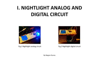
  • 1. I. NIGHTLIGHT ANALOG AND DIGITAL CIRCUIT Fig.1 Nightlight analog circuit Fig.2 Nightlight digital circuit By Wagner Nunes
  • 2. A. Light Depended Resistor (LDR) Fig. 3 Example of LDR component Fig. 4 Example of the LDR function in the exponential decay graphic Fig. 7 Example of an LDR when resistance increases Fig. 6 Example of an LDR when resistance decreases Fig.5 Example of the electrons in the valence band jumping to the conduction band • The LDR is made of a semiconductor material that is layered on an insulating material such as ceramic.
  • 3. B. The Comparator • 1) The Logic: – If (V-) > (V+) => Vout ≈ GND or “0” low (-saturation) – If (V+) < (V-) => Vout ≈ +Vcc or “1” high (+saturation) Fig. 8 Example of a comparator output “0” Fig. 9 Example of a comparator output “1”
  • 4. C. Function of the NPN Bipolar Junction Transistor (BJT) as a Switch • NPN (N stands for negative charge and P stands for positive charge or hole) • BJT(bipolar junction transistor ) is because it involves both of these types of charger. Fig. 11 Example of a transistor tuning the LED onFig. 10 the three regions of a NPN transistor
  • 5. 1) Cut - Off Region Conditions : • Input base current IB= 0 • VBE < 0.7v • Output collector current IC= 0 • Base – Collector junction BC is reversed biased • Base – Emitter junction BE is reversed biased • Maximum collector VCE= VCC Fig. 12 Example of cut - off region conditions
  • 6. 1) Saturation Region Conditions • Input base current (IB) connected to VCC • VBE > 0.7v • Max collector current IC= VCC/RC • Base – Collector junction BC is forward biased • Base – Emitter junction BE is forward biased • VCE= 0 (ideal saturation) Fig. 13 Example of saturation region conditions
  • 7. Calculation for the collector resistor ( ) , base current ( ) , and base resistor( ) IC = 20mA(datasheet) VCE (Sat ) = 0.2V(datasheet) bDC (direct current gain) = 60(datasheet) IC = bDc ´ IB -VCC + IC RC +VLED +VCE(Sat) = 0 -6V + 20mA ´ RC + 3.4V + 0.2V = 0 -2.4V + 20mA ´ RC = 0 RC = 2.4V 20mA =120W IB = IC bDC = 333mA RB = 6V - 0.7V 333mA =16KW IB RB RC
  • 8. D. LED (light emitting diode) Fig. 12 Example of the barrier potential Fig. 14 Example of current in forward direction on a diode Fig. 15 Energy released by the electron of a single photon. Fig.13 An LED will begin to emit light when the on-voltage is exceeded. Fig. 11 Example of a blue 5mm LED
  • 9. Calculation for energy released by the electron of a single photon. h (Plank 's constant) = 6.626 ´10-34 J / s C(Coulomb) = 6. 25´1018 e- c (Speed of light) = 3´108 m / s l (called lambda or wavelength) u ( frequency) eV (electron volts) lu = c u = c l = 3´108 m / s 470 ´10-9 m = 640 ´1012 s-1 E( photon) = hu = (6. 626 ´10-34 J / s)´ (640 ´1012 s-1 ) = 423´110-21 J E(eV ) = E( photon) ´1Coulomb = (423´10-21 J)´ (6.25´1018 e- ) = 2. 6eV
  • 11. II. NIGHTLIGHT DIGITAL CIRCUIT VERSION – BASIC OPERATION • Arduino Function: – There is no analog output on Arduino. Instead it is a digital output (on or off). – If the output is half of the time on and half of the time off, it is said to be 50% duty cycle. – Duty cycle is the percentage of time that the output is on. The output can be 30%, 20%, 10% duty cycle, or any percentage from 0 – 100%. – The Arduino has a technic called pulse width modulation (PMW) that makes its output work as analog.
  • 12. Arduino Function: • In the nightlight device, it allows the LED to fade in and out going from 0 to 255 (8 bits = as a default resolution) value repeating in a loop. • 0 correspond to 0 volts and 255 to 5 volts and any value in between are proportional to those voltages. • Then theses values are sent to the PWM pin (PWM Pins 3, 5, 6, 9, 10, 11) thus fading the LED in and out. 28
  • 13. Arduino Function – Pulse Width Modulation Fig.18 Example of pulse width modulation
  • 14. 1) Formula for Duty Cycle: DutyCycle= TH T ´100% Voltage per step (analogWrite( )) : x=0 ® 255 xsteps how many volts xsteps = x steps 5V 255 steps =19.6mV per step how many volts= x 5V 255 æ è ç ö ø ÷ =
  • 15. E. Arduino Function: • This “function call” passes the read value (argument) from the inputs (A0 to A5) to the function in the library and its return an integer, which is from 0 to 1023 (10 bits = ) as a default resolution). • 0 corresponds to 0V and 1023 to 5V. 210
  • 16. formula to calculate the voltages per step on the input read x = 0 ®1023 xsteps how many volts xsteps = x steps 5V 1024 steps = 4.88mV per step how many volts= x 5V 1024 æ è ç ö ø ÷ =
  • 17. Appendix C Flowchart for the Digital Circuit
  • 18. III. NIGHTLIGHT ANALOG CIRCUIT VERSION VS. NIGHTLIGHT DIGITAL CIRCUIT VERSION NIGHTLIGHT ANALOG CIRCUIT VERSION NIGHTLIGHT DIGITAL CIRCUIT VERSION I spent more time with the digital circuit than the analog one because of my familiarity with it. I improved my lack of skills with Arduino the analog circuit required more space on the board than the digital one due to more parts used.
  • 19. V. COST TO BUILD AND OPERATE NIGHTLIGHT ANALOG CIRCUIT NIGHTLIGHT DIGITAL CIRCUIT costs about $5.70 costs about $26.38, approximately five times more (because of the Arduino ) + Arduino can be used for other applications because it is programmable. Running on 6V (Maui Electric Company), 8 hours per day, the cost is $1.20 per month. Running on 6V battery, 8 hours per day, the cost is $11 per month.
  • 20. Conclusion • As a result, this project spiked my interest even more in electronics hardware, software, and more about technology in general. Consequently, after my associate degree in the ECET, my next academic goal is to earn a bachelor’s degree, become an electronic computer engineer, and perhaps to earn a master degree so I can teach electronics at a university.