SlideShare a Scribd company logo
1 of 24
Download to read offline
US006756838B1
(12) United States Patent (10) Patent N0.: US 6,756,838 B1
Wu et al. (45) Date of Patent: Jun. 29, 2004
(54) CHARGE PUMP BASED VOLTAGE 6,208,197 B1 * 3/2001 Ternullo et a1. .......... .. 327/536
REGULATOR WITH SMART POWER 6,229,161 B1 5/2001 Nemati et al.
REGULATION 6,278,317 B1 * 8/2001 Hsu et al. ................. .. 327/536
6,424,202 B1 7/2002 Bartlett
(75) IIIVGIIIOI‘SZ Dandan Wu, Sunnyvale, (US); OTHER PUBLICATIONS
Plerre Dermy, Nevada City, CA (US)
Jieh—Tsorng Wu, Kuen—Long Chang, “MOS—Charge Pumps
(73) Assignee: T-Ram, Inc., San Jose, CA (US) for LoW Voltage Operation,” IEEE Journal of Solid State
Circuits, vol. 33, No. 4, Apr. 1998, pp. 592—597.
( * ) Notice: Subject to any disclaimer, the term of this * _ _
patent is extended or adjusted under 35 cued by exammer
U'S'C' 154(k)) by 0 days‘ Primary Examiner—Jeffrey ZWeiZig
(21) Appl. No.: 10/391,326 (57) ABSTRACT
(22) Filed; Mal; 18, 2003 A charge pump based voltage regulator With smart poWer
7 regulation employs an architecture that requires that the
(51) Int. Cl. .................................................. G05F 1/10 Charge pump Current be a linear Combination of the load
(52) US Cl- - - - - - - - - - - - - - - - - - - - - - - - - - - -- 327/536 current and a clamp current With a possible offset current.
(58) Field of Search ................................. 327/530, 534, The smart poWer regulation is based on automatic load
327/535, 536, 537 activity (or load current) detection using the clamp current.
The clamp current and the ?ltered charge pump current are
(56) References Cited compared With one another; and the charge pump current is
Us‘ PATENT DOCUMENTS then adJusted accordingly by stepping'the frequency of the
clock driving the charge pump, optimizing the poWer con
5,161,096 A 11/1992 Newman sumption of the entire voltage regulator With varying load
5,399,928 A 3/1995 Lin et a1. activity. The negative voltage regulation is independent of
5,532,640 A 7/1996 Qkunaga the integrated circuit positive supply voltage. In one
11: 1;; gm ct al't t 1 embodiment, a derivative of the desired output voltage is, , amamo 0 e a . -
5,841,314 A 11/1998 Briga? et a1‘ compared W1t1h ~a relfelrence goltageg t5)~ generate afclamp5,946,225 A 8/1999 Ryu et a1‘ current contro s1gna '. ‘n anot er em 0 1ment,t e re erence
6,091,282 A * 7/2000 Kim ......................... .. 327/536 Voltage 15 solely Posmve
6,151,255 A 11/2000 J00 et 211.
6,166,968 A 12/2000 Song 33 Claims, 16 Drawing Sheets
19.
18 16
, (J 26 r___________"1'
CK Charge VN L i_ 08d :
. vco —?3——> Pump 2 a
44 l............“
22
Ipump_sense
LOF<023> Gear
4-— -
Shlft
, Ic|amp_sense I14 512
24
Positive
Vref I Clamp
Regulator
70
——-—--——-—>
Se uence
“a SE;EN ———->
U.S. Patent Jun. 29, 2004 Sheet 1 0f 16 US 6,756,838 B1
6858
005cm+2V
lnwlAl
H
mEEm
H
U.S. Patent Jun. 29, 2004 Sheet 3 0f 16 US 6,756,838 B1
1
z»
m.GE
Acvxcmm52mmAovxcmm52mm
U.S. Patent Jun. 29, 2004 Sheet 4 0f 16 US 6,756,838 B1
FIG.4
------- .
EN reset SET VN (VWL2) -2V
U.S. Patent Jun. 29, 2004 Sheet 6 6f 16 US 6,756,838 B1
0.0E
llullllll.0x0
mmvm
636?yovBEEE25028889:2.c2623.
E2509E6395ad
.F
3Aif
5:02amE250“E51@920omm=o>mémmwz
U.S. Patent Jun. 29, 2004 Sheet 7 0f 16 US 6,756,838 B1
wmulimm
Aonmvmmqdmm3610..
+
JQJ
0
+1
.16l
%552033
I
o<0E950
M23:
2.86ooATIOATIImQ
$6ooATloATllé
86TOATIOATIQs6IATAATINQE0voATloATlE
mEQQQw5538i6*95E2509600>
U.S. Patent Jun. 29, 2004 Sheet 8 0f 16 US 6,756,838 B1
aEza@920669mmE250.32
m.OE
wow
PM
Nov
k
62.5youomm=o>85:5?98n=mm>
U.S. Patent Jun. 29, 2004 Sheet 10 0f 16 US 6,756,838 B1
honqmpm553cm:2AQHmVLOJ
‘ll-I'll
hmuoocoBEEQEBE?zcosamw
2..07.
BHEQESHowohE950+
b29388
+
L0>>On_wwwoxm
/E250+_
4
III623530IIIaEsEmEo
U.S. Patent Jun. 29, 2004 Sheet 11 0f 16 US 6,756,838 B1
Amnovkg
EHEDNOSK
BNosxQHEOO25
hmuoocm66805.2‘.?zcozwow
v.0
mvuZAQV6.2.E15
U.S. Patent Jun. 29, 2004 Sheet 12 0f 16 US 6,756,838 B1
CKtochargepump
ICONCO—-—————> FIG.12
+
lblas
currentDAC
LOF<310>
me.9"
000.0000M000doomé000.?000.0000.0
00nd,.
633
000%000.0
US 6,756,838 B1
000.N000.P.000.T
Sheet 13 0f 16
000.0oomd000._.
Jun. 29, 2004
000.?
P15.E04E049.00
000.N00nd000.0
U.S. Patent
U.S. Patent Jun. 29, 2004 Sheet 14 0f 16 US 6,756,838 B1
E04$649649:22llaEzarm?o
U.S. Patent Jun. 29, 2004 Sheet 15 0f 16 US 6,756,838 B1
2.9"
9.04E04
2.5882
:9;F0695
NmOJmmOJ
623530
U.S. Patent Jun. 29, 2004 Sheet 16 0f 16 US 6,756,838 B1
2..9"
Aumwzv
80.683Q8.“838383838380.0
_________oood.
u
>>>3&2v-83
.4/.___..-_-.-L._-l
oood83
_____________________________________=________________________________._________________________=.83
____
_________________________________________________________________________________________________________________________________-8o.”_______________________________________._
_______________________________________________________________________________________________________-83
____________________________________________________________________________________________________________________________________-
8%
_______________________________________________________________________________________________________________________________________________________-83
______
______________________________________________________________________________________________________________________________________-83
_________._
___________.__________________________________________________________________________________________________-.
._..._..83
$95::I
~08¢E36283__=“_2s:
US 6,756,838 B1
1
CHARGE PUMP BASED VOLTAGE
REGULATOR WITH SMART POWER
REGULATION
BACKGROUND OF THE INVENTION
1. Field of the Invention
This invention relates generally to voltage regulators, and
more particularly to a charge pump based voltage regulator
With smart poWer regulation.
2. Description of the Prior Art
Aconventional SRAM device employs SRAM cells, each
cell consisting of four or six transistors. A thyristor based
SRAM cell consists of only tWo devices, the thyristor itself,
and a pass transistor. An SRAM device comprising thyristor
SRAM cells Will thus be much more compact and much less
costly.
SWitching betWeen the on state and the off state of a
thyristor hoWever, takes rather a long time due to the long
life time of the minority carriers in the P-base. This char
acteristic undesirably limits the speed of operation of a
thyristor-based SRAM. A thinly capacitively coupled thy
ristor (TCCT) to signi?cantly speed up the sWitching has
been disclosed in US. Pat. No. 6,229,161, entitled Semi
conductor capacitively-coupled NDR Device And Its Appli
cations In High-Density High-Speed Memories And In
PoWer SWitches, issued May 8, 2001 to Nemati et al. A
TCCT employs an additional gate closely coupled to a base
region. This gate is coupled to a control line commonly
knoWn as Word line 2 (WL2), Which is pulsed from a
negative voltage to a positive voltage When the TCCT is in
its Write operation. The negative voltage is necessary to
loWer the P-base potential and alloWs the carriers in the
P-base to How out quickly during the Write operation,
signi?cantly expediting the sWitching of TCCT states. FIG.
1 illustrates a TCCT cell in a CMOS process.
Conventional SRAM products based on six-MOSFET
memory cells are poWered-up by a positive voltage supply
and usually do not require a negative voltage source to
operate.
It Would therefore be desirable and advantageous in vieW
of the foregoing to provide a technique to generate an
on-chip negative supply for the WL2 in a TCCT-based
SRAM array from the positive voltage supply poWering-up
the integrated circuit (IC).
BRIEF DESCRIPTION OF THE DRAWINGS
FIG. 1 illustrates a TCCT in series With a pass gate
(NMOSFET) in a CMOS process;
FIG. 2 is a simpli?ed schematic diagram illustrating a
charge pump based negative voltage generator With smart
poWer regulation according to one embodiment of the
present invention;
FIG. 3 is a simpli?ed block diagram illustrating a negative
voltage regulator driving a plurality of WL2s associated
With a plurality of SRAMs;
FIG. 4 shoWs a timing diagram associated With the
negative voltage regulator shoWn in FIG. 2;
FIG. 5 is a schematic diagram illustrating one technique
of providing positive clamp regulator frequency compensa
tion suitable for use With the negative voltage regulator
shoWn in FIG. 2;
FIG. 6 is a schematic diagram illustrating one technique
ofproviding negative voltage charge pump current detection
suitable for use With the negative voltage regulator shoWn in
FIG. 2;
1O
15
25
35
40
45
55
65
2
FIG. 7 is a schematic diagram illustrating one technique
of implementing a VCO and a current DAC for frequency
stepping suitable for use With the negative voltage regulator
shoWn in FIG. 2;
FIG. 8 is a simpli?ed schematic diagram illustrating a
negative voltage regulator using a voltage loop to force a
Word line 2 output voltage according to one embodiment of
the present invention;
FIG. 9 is a schematic diagram illustrating one technique
of providing a gear shift With current comparators and a
sequential thermo encoder suitable for use With the negative
voltage regulator shoWn in FIG. 2;
FIG. 10 is a block diagram illustrating a more simpli?ed
version of the gear shift mechanism depicted in FIG. 9;
FIG. 11 is a more detailed schematic diagram of the
sequential thermo encoder shoWn in FIG. 9;
FIG. 12 is a simpli?ed block diagram the frequency
stepping mechanism associated With the gear shift depicted
in FIG. 9;
FIG. 13 is a timing diagram illustrating gear shift response
to alternating no load and full load conditions for the gear
shift depicted in FIG. 9;
FIG. 14 is a timing diagram illustrating gear shift response
to achieve small poWer stepping for the gear shift depicted
in FIG. 9;
FIG. 15 is a timing diagram illustrating gear shift response
during Wake-up for the gear shift depicted in FIG. 9; and
FIG. 16 is a diagram illustrating the effect of poWer
regulation on pump current for one embodiment of the
negative voltage regulator shoWn in FIG. 2.
While the above-identi?ed draWing ?gures set forth par
ticular embodiments, other embodiments of the present
invention are also contemplated, as noted in the discussion.
In all cases, this disclosure presents illustrated embodiments
of the present invention by Way of representation and not
limitation. Numerous other modi?cations and embodiments
can be devised by those skilled in the art Which fall Within
the scope and spirit of the principles of this invention.
DETAIL DESCRIPTION OF THE INVENTION
Charge pumps (CPs) are commonly used inside an IC to
generate either a negative voltage or a positive voltage larger
than the external supply voltage poWering-up the IC. CPs of
various types (NMOSFET or PMOSFET-based, With or
Without bootstrapping) have been developed since the early
days of silicon-based MOS technologies. They Were also
implemented in bipolar technologies. CPs are notorious for
three undesirable de?ciencies. First and foremost they are
very inef?cient in terms of circuit area and overall poWer
dissipation. They require a large amount of capacitor Which
occupies a large area on an IC (relatively to other circuit
blocks and functions on the IC). Their inef?ciency is further
Worsened by their sensitivity to leakage currents and the
effect of circuit parasitic capacitances. CP poWer ef?ciency
is very loW, often less than 10% and seldom above 25%. The
ef?ciency tends to decrease as the CP output current loading
requirements and the magnitude of the output voltage are
increased. For instance, in order to deliver a 2 mA output
current at an output voltage of approximately 2.0 V (either
beloW the IC ground level, as in the case of the negative
voltage generator (NVG) discussed beloW, or above the
positive supply that is used to poWer-up the IC), the CP
draWs a total current in the order of 25 mA from the IC
external supply.
The second limitation of MOSFET-based CPs is their
inaccurate and unstable output voltage With varying loading
US 6,756,838 B1
3
conditions. This lack of accuracy and stability is due to the
switched capacitor nature of or the charge transfer mecha
nism in CPs. It is further Worsened by the rate of variation
With time in the CP loading conditions. Extended dynamic
loading requires more ?ltering, more CP output storage and
as a consequence more CP internal capacitor for a ?xed
average output load current.
The third major detrimental CP characteristics (Which is
related to the previous tWo) is the limited output current
capability. CP circuits commonly described in specialiZed
technical publications produce output currents in the order
of tens of microamperes or 100 to 200 pA at best. The
loading requirements placed on the WL2 NVG for the
TCCT-based SRAM arrays developed by T-RAM, Inc. is ten
times or one order of magnitude greater than the maximum
capacity commonly reported to this date.
Based on the above considerations, it appears highly
desirable for the technical and commercial viability of
TCCT-based SRAM arrays, either as a standalone IC or a
building block or memory function in a larger IC such as a
Microcontroller (uC), Microprocessor (,uP), Network Pro
cessor (nP), Digital Signal Processor (DSP) or Application
Speci?c Integrated Circuit (ASIC), to implement a NVG by
attaching an output voltage regulator to a negative voltage
CP. Furthermore it is very important that this NVG be
implemented in such a Way that it can conserve poWer and
improve the poWer ef?ciency thereby minimiZing the overall
IC poWer dissipation. Speci?cally, the poWer consumption
of the CP should be adjustable during various operating
modes of the SRAM array, e.g., When the current loading
requirements on the NVG is changed betWeen a minimum
value and a maximum value (either gradually or abruptly),
or continuously at a more or less rapid rate of change, or in
discrete steps of more or less greater height and more or less
closely spaced in time. It Would be even more desirable and
advantageous to provide a general architecture for imple
menting voltage regulation With smart poWer regulation
based on automatic load activity detection Wherein the
architecture and associated methods are independent of the
voltage supply (internal or external) that poWers up the IC.
A number of applications in the ?elds of large and dense
non-volatile memories, photodetectors and image sensors,
specialiZed analog interfaces can greatly bene?t from the
technique and methods described herein.
The various methods of supply voltage regulation and
conversion developed over time in the ?elds of electronic
poWer supply generation, conversion and management have
been classi?ed in tWo major categories: “linear” and
“switch-Mode.” Each category presents a set of graded
advantages. The advantages of the “linear” category are
voltage accuracy, loW-noise ?gures, ease of use and com
plexity management. The primary advantage of the “sWitch
mode” category is poWer efficiency. A subset of the sWitch
mode category is the purely sWitched-capacitor type. CP
falls Within this sub-category. Another subset of sWitch
mode regulator is commonly referred to as a “boost con
verter.” As previously mentioned their accuracy and stability
With load variations is quite loW, although it may be
adequate for certain applications (such as in certain DRAM
and most conventional non-volatile memory technologies).
The linear category is further divided into “drop-out” and
“clamp” subcategories. Linear drop-out Regulators (LDO)
take an input supply voltage and reduce it a loWer absolute
value ie less negative from an input beloW the ground
plane, or less positive from an input above the ground plane.
LDO operates on the principle of supplying more or less
current to the load and modulating the conductance of a pass
10
15
25
35
40
45
55
65
4
transistor Which usually is a large poWer device. LDO
regulators can be further sub-categoriZed by the type and
biasing of the voltage drop-out device, either NMOS or
PMOS, NPN or PNP bipolar transistors, biased either as a
voltage folloWer in a common drain or collector
con?guration, or as a phase inverter in a common source or
emitter con?guration. Each of these circuit topologies pre
sents its speci?c advantage When considering the quality and
requirements of load and line regulations.
In contrast to a LDO regulator, a clamp regulator operates
on the principle of adding a dummy load in parallel to the
speci?ed regulator output load, and modulating the conduc
tance of this dummy load to compensate for variations in the
regulator output load. The dummy load is a smaller device
than the voltage dropout poWer transistor and therefore
modulating its drive requires less poWer. In cases Where
output load variations are limited in amplitude, or in cases
Where they are very rapid (also referred to as high dynamic
output loads), a clamp regulator is more poWer ef?cient. This
is achieved by maintaining the voltage dropout pass
transistor under a constant bias rather than modulating it in
the LDO regulator con?guration. In certain cases of a high
dynamic load With large ?uctuations, combining a LDO and
a clamp regulator in a dual regulation loop is an appropriate
solution. The stability of a dual loop system must be
carefully studied and sometimes trimmed. Therefore such
hybrid technique is usually considered only When the load
variations are someWhat predictable and can be character
iZed Within de?nable limits in time and amplitude.
Another advantage of a clamp regulator is that it is more
compact and ef?cient. A clamp regulator to maintain the
output voltage of a CP supplying the negative WL2 voltage
to the TCCT-based SRAM array, or producing a positive
voltage greater than the IC supply voltage, is a more feasible
and/or attractive solution When compared to an LDO regu
lator (Which Would require a CP output voltage of greater
magnitude than the output voltage speci?ed in the
application), or to a boost converter (Which Would require a
larger amount of sWitched-capacitor Within the IC or capaci
tors and other magnetic components and even specialiZed
diodes external to the IC). Also this clamp regulation tech
nique readily lends itself, Without further increase in the
overhead poWer dissipation and the CP output voltage, to the
attachment of tWo relatively small sensing current mirrors.
One is connected in parallel With the CP output blocking
transistor. The other is connected in parallel With one of the
transistors in the current clamping branch of the clamp
regulator attached to the CP output. The output of these tWo
current sensors can be used to not only monitor the load
current, but also as the feedback variable in a separate
control loop to maintain the CP activity and resulting poWer
dissipation at the minimum level to insure proper operation
and stability of the NVG. This second loop is a current loop,
as the feedback variable being measured and controlled is a
difference betWeen tWo sensed currents.
The present invention is directed to a charge pump based
NVG With clamp-type output voltage regulation and With
smart poWer regulation of the charge pump current to
optimiZe the overall poWer ef?ciency of the NVG. The
general architecture relies on the fact that the charge pump
delivers a current equal to a linear combination of the load
current and the current through the clamp of the voltage
regulator or clamp current. Note that this linear combination
also includes the possible presence of an offset current. The
smart poWer regulation is based on automatic detection or
sensing of both the clamp current and the charge pump
output current, and a comparison of these tWo currents. The
US 6,756,838 B1
5
clamp current and the ?ltered charge pump current are
compared With one another, and the charge pump current is
then adjusted accordingly by stepping the frequency of the
clock driving the charge pump, optimiZing the poWer con
sumption of the entire NVG With varying load activity.
According to one embodiment, a charge pump based
negative voltage generator (CPNVG) is provided that is
responsive to an output load current and its variations,
Wherein the clamp current is the difference betWeen the
charge pump output current and the CPNVG output load
current.
Looking at FIG. 2, a simpli?ed block diagram illustrates
a negative voltage regulator 10 according to one embodi
ment of the present invention. It shall be understood
hoWever, that the present invention is not so limited, and that
although the particular embodiments described herein beloW
refer to a negative voltage regulator, the present invention
applies equally to both positive and negative voltage regu
lators. With continued reference to FIG. 2, negative voltage
regulator 10 may, for example, generate an on-chip negative
supply for the Word line 2 (WL2) in a TCCT-based SRAM
array. Regulator 10 is based on dual loop regulation con
sisting of a voltage loop 12 and a current loop 14. Since
these tWo loops 12, 14 are closely coupled Within one
feedback circuit, they Will herein after be collectively
referred to as a voltage/current loop. The main building
blocks associated With negative voltage regulator 10 include
a negative voltage charge pump 16, a voltage-controlled
oscillator (VCO) 18 and a positive clamp regulator fre
quency compensation circuit 70.
A current loop segment 22 is employed by the negative
voltage regulator 10 to minimiZe poWer consumption in
various operating modes of the load e.g., SRAM array
discussed herein before. The current loop segment 22
includes a gear shift circuit 24 using direct detection of
charge pump 16 current as a feedback parameter.
The negative voltage regulator 10 generates a negative
voltage supply VN 26 that is also shoWn in FIG. 3 Which is
a simpli?ed block diagram illustrating the negative voltage
regulator 10 driving a plurality of Word line 2 (WL2) drivers
associated With a plurality of SRAM banks 28, 30, 32.
FIG. 4 shoWs a timing diagram associated With the
negative voltage regulator 10 shoWn in FIG. 2. The negative
voltage supply VN 26 sequence can be seen to commence
folloWing enable EN and internal reset pulses, at Which time
the negative voltage supply VN 26 begins to drop from its
initial value of 0V until reaching its ?nal value of —2V. A
signal named SET is asserted after VN ?rst crosses its
desired ?nal value.
Looking noW at FIG. 6, a schematic diagram illustrates
one technique of providing negative voltage charge pump
current detection suitable for use With the negative voltage
regulator 10 shoWn in FIG. 2. The negative voltage charge
pump 16 comprises four stages 34, 36, 38, 40 and a current
mirror 42. Each stage 34—40 most preferably provides an
equal amount of voltage drop; Wherein the total voltage drop
depends on the sWing of the input clock (enumerated as 44
in FIG. 2), threshold voltages of the MOS devices, the ratio
betWeen the main capacitances and the parasitic
capacitances, the frequency of the input clock 44 and the
load current. The NMOS current mirror 42 at the output of
the charge pump 16 is employed to detect the current
through the charge pump 16. The current detection is then
used to achieve the desired poWer regulation as described
further herein beloW. A cascode transistor N1 (112) is
coupled in series to the mirror transistor 110. The gate of
10
25
35
40
45
55
65
6
cascode transistor 112 is biased at ground or an appropriate
voltage to both isolate the mirror transistor 110 from the
increased charge pump output voltage and improve the
output impedance of the current mirror 42.
FIG. 7 is a schematic diagram illustrating one technique
of implementing a VCO 18 and a current DAC 50 for
frequency stepping suitable for use With the negative voltage
regulator 10 shoWn in FIG. 2. The VCO 18 is a ring
oscillator comprising ?ve stages of starved inverters 52, 54,
56, 58, 60. It can be a voltage-controlled oscillator (VCO),
current-controlled oscillator (ICO) or, in a broader sense,
any oscillator Whose frequency is tunable via an input
control signal or signals. The oscillator in FIG. 7 is con?g
ured as an ICO. The current is programmed via LOF<0:3>
62 to discretely tune the frequency of the output clock. The
present inventors found an oscillator 18 frequency range of
about 50 MHZ through about 300 MHZ to provide Workable
results. TWo adjacent oscillator 18 clock phases are used to
generate a pair of non-overlapping clocks driving the charge
pump 16.
With reference noW to FIG. 5, a schematic diagram
illustrates one technique of providing positive clamp regu
lator frequency compensation suitable for use With the
negative voltage regulator 10 shoWn in FIG. 2. The positive
clamp regulation loop 70 regulates the negative voltage VN
26 and further supplies the clamp current 72. Avariation in
the load current Will cause a disturbance in VN 26. An
OPAMP 20 in the loop compares a reference voltage 74 With
a voltage VX 76 derived from the negative voltage 26. The
OPAMP 20 then regulates the clamp current 72 in response
to the outcome of the comparison. The charge pump 16
current Ipump is thus continuously adjusted since it is the sum
of the load current and clamp current. Notice in FIG. 5 that
I is a measurement of and proportional topumpisense Ipump;
clampismse is a measurement of and proportional to Idamp.
In one embodiment, the bandWidth of the voltage/current
regulation loop 70 Was found by the present inventors to be
about 7 MHZ through about 13 MHZ With VCC at 1.8V
(phase margin 40°—58°), and to be about 10 MHZ through
about 17 MHZ With VCC at 2.5V (phase margin 38°—50°),
across process, supply voltage and temperature corners.
More speci?cally, the regulation of the negative voltage
VN 26 is performed via the voltage feedback loop 12 (not by
the current loop segment) With positive current clamping. A
voltage divider extracts a positive voltage VX 76 from the
negative voltage VN 26, and an auxiliary voltage Vtop, such
that the extracted voltage is proportional to the negative
voltage VN 26, Wherein
and Where 0<(X<1. OPAMP 20 compares the extracted
voltage With a readily available positive reference voltage
VREF 74 and ampli?es the difference. A PMOS 77 driven
by this OPAMP 20 in turn generates a current Idamp 72 that
is proportional to the comparison result. A cascode MOS
transistor M2 (78) coupled in series With PMOS 77 isolates
PMOS 77 from the increased regulator output voltage to
prevent voltage breakdoWn of PMOS 77. The gate of
cascode MOS transistor 78 is biased at ground or any
appropriate voltage to maximiZe, Without breakdoWn, the
voltage drop betWeen the drain and source of PMOS 77. The
cascode MOS transistor 78 also stands to improve the gain
of the positive clamp regulator loop.
A Miller compensation capacitor 120 in series With a
resistor 122 is used to realiZe frequency compensation or
stabiliZation of the positive clamp regulator loop. Note this
U Pataent # 6756838
U Pataent # 6756838
U Pataent # 6756838
U Pataent # 6756838

More Related Content

What's hot

Hutchison effect more info
Hutchison effect   more infoHutchison effect   more info
Hutchison effect more infoJohn Hutchison
 
Danapur Electrical LayOut-Final Model
Danapur Electrical LayOut-Final ModelDanapur Electrical LayOut-Final Model
Danapur Electrical LayOut-Final ModelMd Ishteyaque
 
Inertia dynamics ac_motor_brake_specsheet
Inertia dynamics ac_motor_brake_specsheetInertia dynamics ac_motor_brake_specsheet
Inertia dynamics ac_motor_brake_specsheetElectromate
 
EDS22719 MDB (PAGE 1)
EDS22719 MDB (PAGE 1)EDS22719 MDB (PAGE 1)
EDS22719 MDB (PAGE 1)MARK IMPEY
 
Vw beta5
Vw beta5Vw beta5
Vw beta5TDCSoft
 

What's hot (8)

Atmoselecgen
AtmoselecgenAtmoselecgen
Atmoselecgen
 
Hutchison effect more info
Hutchison effect   more infoHutchison effect   more info
Hutchison effect more info
 
Danapur Electrical LayOut-Final Model
Danapur Electrical LayOut-Final ModelDanapur Electrical LayOut-Final Model
Danapur Electrical LayOut-Final Model
 
Inertia dynamics ac_motor_brake_specsheet
Inertia dynamics ac_motor_brake_specsheetInertia dynamics ac_motor_brake_specsheet
Inertia dynamics ac_motor_brake_specsheet
 
Ciclotron pwp20000 2 h
Ciclotron   pwp20000 2 hCiclotron   pwp20000 2 h
Ciclotron pwp20000 2 h
 
Gis basics
Gis basicsGis basics
Gis basics
 
EDS22719 MDB (PAGE 1)
EDS22719 MDB (PAGE 1)EDS22719 MDB (PAGE 1)
EDS22719 MDB (PAGE 1)
 
Vw beta5
Vw beta5Vw beta5
Vw beta5
 

Similar to U Pataent # 6756838

IRJET-CUK Converter Based PV Module for Excitation Ff Synchronous Machine
IRJET-CUK Converter Based PV Module for Excitation Ff Synchronous MachineIRJET-CUK Converter Based PV Module for Excitation Ff Synchronous Machine
IRJET-CUK Converter Based PV Module for Excitation Ff Synchronous MachineIRJET Journal
 
Stability Analysis of DC-link Voltage Control on Autonomous Micro Hydro Power...
Stability Analysis of DC-link Voltage Control on Autonomous Micro Hydro Power...Stability Analysis of DC-link Voltage Control on Autonomous Micro Hydro Power...
Stability Analysis of DC-link Voltage Control on Autonomous Micro Hydro Power...IAES-IJPEDS
 
E041116369
E041116369E041116369
E041116369IOSR-JEN
 
Design, Simulation and Implementation of Flyback based, True Single Stage, Is...
Design, Simulation and Implementation of Flyback based, True Single Stage, Is...Design, Simulation and Implementation of Flyback based, True Single Stage, Is...
Design, Simulation and Implementation of Flyback based, True Single Stage, Is...IJMER
 
Three-Level DTC Based on Fuzzy Logic and Neural Network of Sensorless DSSM Us...
Three-Level DTC Based on Fuzzy Logic and Neural Network of Sensorless DSSM Us...Three-Level DTC Based on Fuzzy Logic and Neural Network of Sensorless DSSM Us...
Three-Level DTC Based on Fuzzy Logic and Neural Network of Sensorless DSSM Us...IJPEDS-IAES
 
Analysis of Commutation Torque Ripple Minimization for Brushless DC Motor Bas...
Analysis of Commutation Torque Ripple Minimization for Brushless DC Motor Bas...Analysis of Commutation Torque Ripple Minimization for Brushless DC Motor Bas...
Analysis of Commutation Torque Ripple Minimization for Brushless DC Motor Bas...IJERA Editor
 
Transient Dynamic Analyzing for Induction Motor Design Based on combine Simul...
Transient Dynamic Analyzing for Induction Motor Design Based on combine Simul...Transient Dynamic Analyzing for Induction Motor Design Based on combine Simul...
Transient Dynamic Analyzing for Induction Motor Design Based on combine Simul...IJERA Editor
 
Implementation of Three phase SPWM Inverter with Minimum Number of Power Elec...
Implementation of Three phase SPWM Inverter with Minimum Number of Power Elec...Implementation of Three phase SPWM Inverter with Minimum Number of Power Elec...
Implementation of Three phase SPWM Inverter with Minimum Number of Power Elec...IJMTST Journal
 
A dual pulse-clock double edge triggered flip-flop
A dual pulse-clock double edge triggered flip-flopA dual pulse-clock double edge triggered flip-flop
A dual pulse-clock double edge triggered flip-flopKavitha Reddy
 
Fuzzy-PI Torque and Flux Controllers for DTC with Multilevel Inverter of Indu...
Fuzzy-PI Torque and Flux Controllers for DTC with Multilevel Inverter of Indu...Fuzzy-PI Torque and Flux Controllers for DTC with Multilevel Inverter of Indu...
Fuzzy-PI Torque and Flux Controllers for DTC with Multilevel Inverter of Indu...IJPEDS-IAES
 
Implementation of PWM Control of DC Split Converter Fed Switched Reluctance M...
Implementation of PWM Control of DC Split Converter Fed Switched Reluctance M...Implementation of PWM Control of DC Split Converter Fed Switched Reluctance M...
Implementation of PWM Control of DC Split Converter Fed Switched Reluctance M...IJECEIAES
 

Similar to U Pataent # 6756838 (20)

IRJET-CUK Converter Based PV Module for Excitation Ff Synchronous Machine
IRJET-CUK Converter Based PV Module for Excitation Ff Synchronous MachineIRJET-CUK Converter Based PV Module for Excitation Ff Synchronous Machine
IRJET-CUK Converter Based PV Module for Excitation Ff Synchronous Machine
 
Stability Analysis of DC-link Voltage Control on Autonomous Micro Hydro Power...
Stability Analysis of DC-link Voltage Control on Autonomous Micro Hydro Power...Stability Analysis of DC-link Voltage Control on Autonomous Micro Hydro Power...
Stability Analysis of DC-link Voltage Control on Autonomous Micro Hydro Power...
 
E041116369
E041116369E041116369
E041116369
 
Design, Simulation and Implementation of Flyback based, True Single Stage, Is...
Design, Simulation and Implementation of Flyback based, True Single Stage, Is...Design, Simulation and Implementation of Flyback based, True Single Stage, Is...
Design, Simulation and Implementation of Flyback based, True Single Stage, Is...
 
JSAEM
JSAEMJSAEM
JSAEM
 
Three-Level DTC Based on Fuzzy Logic and Neural Network of Sensorless DSSM Us...
Three-Level DTC Based on Fuzzy Logic and Neural Network of Sensorless DSSM Us...Three-Level DTC Based on Fuzzy Logic and Neural Network of Sensorless DSSM Us...
Three-Level DTC Based on Fuzzy Logic and Neural Network of Sensorless DSSM Us...
 
Analysis of Commutation Torque Ripple Minimization for Brushless DC Motor Bas...
Analysis of Commutation Torque Ripple Minimization for Brushless DC Motor Bas...Analysis of Commutation Torque Ripple Minimization for Brushless DC Motor Bas...
Analysis of Commutation Torque Ripple Minimization for Brushless DC Motor Bas...
 
Bldc
BldcBldc
Bldc
 
Transient Dynamic Analyzing for Induction Motor Design Based on combine Simul...
Transient Dynamic Analyzing for Induction Motor Design Based on combine Simul...Transient Dynamic Analyzing for Induction Motor Design Based on combine Simul...
Transient Dynamic Analyzing for Induction Motor Design Based on combine Simul...
 
Implementation of Three phase SPWM Inverter with Minimum Number of Power Elec...
Implementation of Three phase SPWM Inverter with Minimum Number of Power Elec...Implementation of Three phase SPWM Inverter with Minimum Number of Power Elec...
Implementation of Three phase SPWM Inverter with Minimum Number of Power Elec...
 
A dual pulse-clock double edge triggered flip-flop
A dual pulse-clock double edge triggered flip-flopA dual pulse-clock double edge triggered flip-flop
A dual pulse-clock double edge triggered flip-flop
 
C05311115
C05311115C05311115
C05311115
 
Modeling & Analysis of a Novel Adaptive Hysteresis Band Controller for Boost ...
Modeling & Analysis of a Novel Adaptive Hysteresis Band Controller for Boost ...Modeling & Analysis of a Novel Adaptive Hysteresis Band Controller for Boost ...
Modeling & Analysis of a Novel Adaptive Hysteresis Band Controller for Boost ...
 
Fuzzy-PI Torque and Flux Controllers for DTC with Multilevel Inverter of Indu...
Fuzzy-PI Torque and Flux Controllers for DTC with Multilevel Inverter of Indu...Fuzzy-PI Torque and Flux Controllers for DTC with Multilevel Inverter of Indu...
Fuzzy-PI Torque and Flux Controllers for DTC with Multilevel Inverter of Indu...
 
Implementation of PWM Control of DC Split Converter Fed Switched Reluctance M...
Implementation of PWM Control of DC Split Converter Fed Switched Reluctance M...Implementation of PWM Control of DC Split Converter Fed Switched Reluctance M...
Implementation of PWM Control of DC Split Converter Fed Switched Reluctance M...
 
5341 5345.output
5341 5345.output5341 5345.output
5341 5345.output
 
5341 5345.output
5341 5345.output5341 5345.output
5341 5345.output
 
[IJET V2I5P12] Authors: Mr. Harikrishnan U, Dr. Bos Mathew Jos, Mr.Thomas P R...
[IJET V2I5P12] Authors: Mr. Harikrishnan U, Dr. Bos Mathew Jos, Mr.Thomas P R...[IJET V2I5P12] Authors: Mr. Harikrishnan U, Dr. Bos Mathew Jos, Mr.Thomas P R...
[IJET V2I5P12] Authors: Mr. Harikrishnan U, Dr. Bos Mathew Jos, Mr.Thomas P R...
 
2002 15
2002 152002 15
2002 15
 
Ijetcas14 641
Ijetcas14 641Ijetcas14 641
Ijetcas14 641
 

Recently uploaded

Apidays New York 2024 - Scaling API-first by Ian Reasor and Radu Cotescu, Adobe
Apidays New York 2024 - Scaling API-first by Ian Reasor and Radu Cotescu, AdobeApidays New York 2024 - Scaling API-first by Ian Reasor and Radu Cotescu, Adobe
Apidays New York 2024 - Scaling API-first by Ian Reasor and Radu Cotescu, Adobeapidays
 
Axa Assurance Maroc - Insurer Innovation Award 2024
Axa Assurance Maroc - Insurer Innovation Award 2024Axa Assurance Maroc - Insurer Innovation Award 2024
Axa Assurance Maroc - Insurer Innovation Award 2024The Digital Insurer
 
AWS Community Day CPH - Three problems of Terraform
AWS Community Day CPH - Three problems of TerraformAWS Community Day CPH - Three problems of Terraform
AWS Community Day CPH - Three problems of TerraformAndrey Devyatkin
 
ICT role in 21st century education and its challenges
ICT role in 21st century education and its challengesICT role in 21st century education and its challenges
ICT role in 21st century education and its challengesrafiqahmad00786416
 
DBX First Quarter 2024 Investor Presentation
DBX First Quarter 2024 Investor PresentationDBX First Quarter 2024 Investor Presentation
DBX First Quarter 2024 Investor PresentationDropbox
 
Rising Above_ Dubai Floods and the Fortitude of Dubai International Airport.pdf
Rising Above_ Dubai Floods and the Fortitude of Dubai International Airport.pdfRising Above_ Dubai Floods and the Fortitude of Dubai International Airport.pdf
Rising Above_ Dubai Floods and the Fortitude of Dubai International Airport.pdfOrbitshub
 
EMPOWERMENT TECHNOLOGY GRADE 11 QUARTER 2 REVIEWER
EMPOWERMENT TECHNOLOGY GRADE 11 QUARTER 2 REVIEWEREMPOWERMENT TECHNOLOGY GRADE 11 QUARTER 2 REVIEWER
EMPOWERMENT TECHNOLOGY GRADE 11 QUARTER 2 REVIEWERMadyBayot
 
CNIC Information System with Pakdata Cf In Pakistan
CNIC Information System with Pakdata Cf In PakistanCNIC Information System with Pakdata Cf In Pakistan
CNIC Information System with Pakdata Cf In Pakistandanishmna97
 
Emergent Methods: Multi-lingual narrative tracking in the news - real-time ex...
Emergent Methods: Multi-lingual narrative tracking in the news - real-time ex...Emergent Methods: Multi-lingual narrative tracking in the news - real-time ex...
Emergent Methods: Multi-lingual narrative tracking in the news - real-time ex...Zilliz
 
Apidays New York 2024 - The Good, the Bad and the Governed by David O'Neill, ...
Apidays New York 2024 - The Good, the Bad and the Governed by David O'Neill, ...Apidays New York 2024 - The Good, the Bad and the Governed by David O'Neill, ...
Apidays New York 2024 - The Good, the Bad and the Governed by David O'Neill, ...apidays
 
Corporate and higher education May webinar.pptx
Corporate and higher education May webinar.pptxCorporate and higher education May webinar.pptx
Corporate and higher education May webinar.pptxRustici Software
 
Modular Monolith - a Practical Alternative to Microservices @ Devoxx UK 2024
Modular Monolith - a Practical Alternative to Microservices @ Devoxx UK 2024Modular Monolith - a Practical Alternative to Microservices @ Devoxx UK 2024
Modular Monolith - a Practical Alternative to Microservices @ Devoxx UK 2024Victor Rentea
 
TrustArc Webinar - Unlock the Power of AI-Driven Data Discovery
TrustArc Webinar - Unlock the Power of AI-Driven Data DiscoveryTrustArc Webinar - Unlock the Power of AI-Driven Data Discovery
TrustArc Webinar - Unlock the Power of AI-Driven Data DiscoveryTrustArc
 
Cyberprint. Dark Pink Apt Group [EN].pdf
Cyberprint. Dark Pink Apt Group [EN].pdfCyberprint. Dark Pink Apt Group [EN].pdf
Cyberprint. Dark Pink Apt Group [EN].pdfOverkill Security
 
Spring Boot vs Quarkus the ultimate battle - DevoxxUK
Spring Boot vs Quarkus the ultimate battle - DevoxxUKSpring Boot vs Quarkus the ultimate battle - DevoxxUK
Spring Boot vs Quarkus the ultimate battle - DevoxxUKJago de Vreede
 
Strategies for Landing an Oracle DBA Job as a Fresher
Strategies for Landing an Oracle DBA Job as a FresherStrategies for Landing an Oracle DBA Job as a Fresher
Strategies for Landing an Oracle DBA Job as a FresherRemote DBA Services
 
Biography Of Angeliki Cooney | Senior Vice President Life Sciences | Albany, ...
Biography Of Angeliki Cooney | Senior Vice President Life Sciences | Albany, ...Biography Of Angeliki Cooney | Senior Vice President Life Sciences | Albany, ...
Biography Of Angeliki Cooney | Senior Vice President Life Sciences | Albany, ...Angeliki Cooney
 
Artificial Intelligence Chap.5 : Uncertainty
Artificial Intelligence Chap.5 : UncertaintyArtificial Intelligence Chap.5 : Uncertainty
Artificial Intelligence Chap.5 : UncertaintyKhushali Kathiriya
 
Architecting Cloud Native Applications
Architecting Cloud Native ApplicationsArchitecting Cloud Native Applications
Architecting Cloud Native ApplicationsWSO2
 

Recently uploaded (20)

Apidays New York 2024 - Scaling API-first by Ian Reasor and Radu Cotescu, Adobe
Apidays New York 2024 - Scaling API-first by Ian Reasor and Radu Cotescu, AdobeApidays New York 2024 - Scaling API-first by Ian Reasor and Radu Cotescu, Adobe
Apidays New York 2024 - Scaling API-first by Ian Reasor and Radu Cotescu, Adobe
 
Axa Assurance Maroc - Insurer Innovation Award 2024
Axa Assurance Maroc - Insurer Innovation Award 2024Axa Assurance Maroc - Insurer Innovation Award 2024
Axa Assurance Maroc - Insurer Innovation Award 2024
 
AWS Community Day CPH - Three problems of Terraform
AWS Community Day CPH - Three problems of TerraformAWS Community Day CPH - Three problems of Terraform
AWS Community Day CPH - Three problems of Terraform
 
ICT role in 21st century education and its challenges
ICT role in 21st century education and its challengesICT role in 21st century education and its challenges
ICT role in 21st century education and its challenges
 
DBX First Quarter 2024 Investor Presentation
DBX First Quarter 2024 Investor PresentationDBX First Quarter 2024 Investor Presentation
DBX First Quarter 2024 Investor Presentation
 
Rising Above_ Dubai Floods and the Fortitude of Dubai International Airport.pdf
Rising Above_ Dubai Floods and the Fortitude of Dubai International Airport.pdfRising Above_ Dubai Floods and the Fortitude of Dubai International Airport.pdf
Rising Above_ Dubai Floods and the Fortitude of Dubai International Airport.pdf
 
EMPOWERMENT TECHNOLOGY GRADE 11 QUARTER 2 REVIEWER
EMPOWERMENT TECHNOLOGY GRADE 11 QUARTER 2 REVIEWEREMPOWERMENT TECHNOLOGY GRADE 11 QUARTER 2 REVIEWER
EMPOWERMENT TECHNOLOGY GRADE 11 QUARTER 2 REVIEWER
 
CNIC Information System with Pakdata Cf In Pakistan
CNIC Information System with Pakdata Cf In PakistanCNIC Information System with Pakdata Cf In Pakistan
CNIC Information System with Pakdata Cf In Pakistan
 
Emergent Methods: Multi-lingual narrative tracking in the news - real-time ex...
Emergent Methods: Multi-lingual narrative tracking in the news - real-time ex...Emergent Methods: Multi-lingual narrative tracking in the news - real-time ex...
Emergent Methods: Multi-lingual narrative tracking in the news - real-time ex...
 
Apidays New York 2024 - The Good, the Bad and the Governed by David O'Neill, ...
Apidays New York 2024 - The Good, the Bad and the Governed by David O'Neill, ...Apidays New York 2024 - The Good, the Bad and the Governed by David O'Neill, ...
Apidays New York 2024 - The Good, the Bad and the Governed by David O'Neill, ...
 
Corporate and higher education May webinar.pptx
Corporate and higher education May webinar.pptxCorporate and higher education May webinar.pptx
Corporate and higher education May webinar.pptx
 
Modular Monolith - a Practical Alternative to Microservices @ Devoxx UK 2024
Modular Monolith - a Practical Alternative to Microservices @ Devoxx UK 2024Modular Monolith - a Practical Alternative to Microservices @ Devoxx UK 2024
Modular Monolith - a Practical Alternative to Microservices @ Devoxx UK 2024
 
TrustArc Webinar - Unlock the Power of AI-Driven Data Discovery
TrustArc Webinar - Unlock the Power of AI-Driven Data DiscoveryTrustArc Webinar - Unlock the Power of AI-Driven Data Discovery
TrustArc Webinar - Unlock the Power of AI-Driven Data Discovery
 
Cyberprint. Dark Pink Apt Group [EN].pdf
Cyberprint. Dark Pink Apt Group [EN].pdfCyberprint. Dark Pink Apt Group [EN].pdf
Cyberprint. Dark Pink Apt Group [EN].pdf
 
Spring Boot vs Quarkus the ultimate battle - DevoxxUK
Spring Boot vs Quarkus the ultimate battle - DevoxxUKSpring Boot vs Quarkus the ultimate battle - DevoxxUK
Spring Boot vs Quarkus the ultimate battle - DevoxxUK
 
Strategies for Landing an Oracle DBA Job as a Fresher
Strategies for Landing an Oracle DBA Job as a FresherStrategies for Landing an Oracle DBA Job as a Fresher
Strategies for Landing an Oracle DBA Job as a Fresher
 
+971581248768>> SAFE AND ORIGINAL ABORTION PILLS FOR SALE IN DUBAI AND ABUDHA...
+971581248768>> SAFE AND ORIGINAL ABORTION PILLS FOR SALE IN DUBAI AND ABUDHA...+971581248768>> SAFE AND ORIGINAL ABORTION PILLS FOR SALE IN DUBAI AND ABUDHA...
+971581248768>> SAFE AND ORIGINAL ABORTION PILLS FOR SALE IN DUBAI AND ABUDHA...
 
Biography Of Angeliki Cooney | Senior Vice President Life Sciences | Albany, ...
Biography Of Angeliki Cooney | Senior Vice President Life Sciences | Albany, ...Biography Of Angeliki Cooney | Senior Vice President Life Sciences | Albany, ...
Biography Of Angeliki Cooney | Senior Vice President Life Sciences | Albany, ...
 
Artificial Intelligence Chap.5 : Uncertainty
Artificial Intelligence Chap.5 : UncertaintyArtificial Intelligence Chap.5 : Uncertainty
Artificial Intelligence Chap.5 : Uncertainty
 
Architecting Cloud Native Applications
Architecting Cloud Native ApplicationsArchitecting Cloud Native Applications
Architecting Cloud Native Applications
 

U Pataent # 6756838

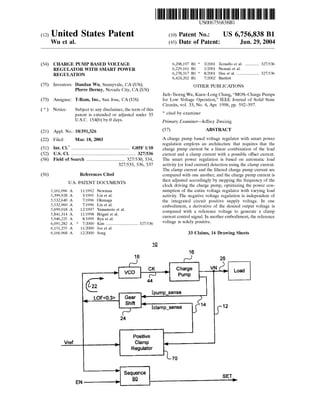
  • 1. US006756838B1 (12) United States Patent (10) Patent N0.: US 6,756,838 B1 Wu et al. (45) Date of Patent: Jun. 29, 2004 (54) CHARGE PUMP BASED VOLTAGE 6,208,197 B1 * 3/2001 Ternullo et a1. .......... .. 327/536 REGULATOR WITH SMART POWER 6,229,161 B1 5/2001 Nemati et al. REGULATION 6,278,317 B1 * 8/2001 Hsu et al. ................. .. 327/536 6,424,202 B1 7/2002 Bartlett (75) IIIVGIIIOI‘SZ Dandan Wu, Sunnyvale, (US); OTHER PUBLICATIONS Plerre Dermy, Nevada City, CA (US) Jieh—Tsorng Wu, Kuen—Long Chang, “MOS—Charge Pumps (73) Assignee: T-Ram, Inc., San Jose, CA (US) for LoW Voltage Operation,” IEEE Journal of Solid State Circuits, vol. 33, No. 4, Apr. 1998, pp. 592—597. ( * ) Notice: Subject to any disclaimer, the term of this * _ _ patent is extended or adjusted under 35 cued by exammer U'S'C' 154(k)) by 0 days‘ Primary Examiner—Jeffrey ZWeiZig (21) Appl. No.: 10/391,326 (57) ABSTRACT (22) Filed; Mal; 18, 2003 A charge pump based voltage regulator With smart poWer 7 regulation employs an architecture that requires that the (51) Int. Cl. .................................................. G05F 1/10 Charge pump Current be a linear Combination of the load (52) US Cl- - - - - - - - - - - - - - - - - - - - - - - - - - - -- 327/536 current and a clamp current With a possible offset current. (58) Field of Search ................................. 327/530, 534, The smart poWer regulation is based on automatic load 327/535, 536, 537 activity (or load current) detection using the clamp current. The clamp current and the ?ltered charge pump current are (56) References Cited compared With one another; and the charge pump current is Us‘ PATENT DOCUMENTS then adJusted accordingly by stepping'the frequency of the clock driving the charge pump, optimizing the poWer con 5,161,096 A 11/1992 Newman sumption of the entire voltage regulator With varying load 5,399,928 A 3/1995 Lin et a1. activity. The negative voltage regulation is independent of 5,532,640 A 7/1996 Qkunaga the integrated circuit positive supply voltage. In one 11: 1;; gm ct al't t 1 embodiment, a derivative of the desired output voltage is, , amamo 0 e a . - 5,841,314 A 11/1998 Briga? et a1‘ compared W1t1h ~a relfelrence goltageg t5)~ generate afclamp5,946,225 A 8/1999 Ryu et a1‘ current contro s1gna '. ‘n anot er em 0 1ment,t e re erence 6,091,282 A * 7/2000 Kim ......................... .. 327/536 Voltage 15 solely Posmve 6,151,255 A 11/2000 J00 et 211. 6,166,968 A 12/2000 Song 33 Claims, 16 Drawing Sheets 19. 18 16 , (J 26 r___________"1' CK Charge VN L i_ 08d : . vco —?3——> Pump 2 a 44 l............“ 22 Ipump_sense LOF<023> Gear 4-— - Shlft , Ic|amp_sense I14 512 24 Positive Vref I Clamp Regulator 70 ——-—--——-—> Se uence “a SE;EN ———->
  • 2. U.S. Patent Jun. 29, 2004 Sheet 1 0f 16 US 6,756,838 B1 6858 005cm+2V lnwlAl H mEEm H
  • 3.
  • 4. U.S. Patent Jun. 29, 2004 Sheet 3 0f 16 US 6,756,838 B1 1 z» m.GE Acvxcmm52mmAovxcmm52mm
  • 5. U.S. Patent Jun. 29, 2004 Sheet 4 0f 16 US 6,756,838 B1 FIG.4 ------- . EN reset SET VN (VWL2) -2V
  • 6.
  • 7. U.S. Patent Jun. 29, 2004 Sheet 6 6f 16 US 6,756,838 B1 0.0E llullllll.0x0 mmvm 636?yovBEEE25028889:2.c2623. E2509E6395ad .F 3Aif 5:02amE250“E51@920omm=o>mémmwz
  • 8. U.S. Patent Jun. 29, 2004 Sheet 7 0f 16 US 6,756,838 B1 wmulimm Aonmvmmqdmm3610.. + JQJ 0 +1 .16l %552033 I o<0E950 M23: 2.86ooATIOATIImQ $6ooATloATllé 86TOATIOATIQs6IATAATINQE0voATloATlE mEQQQw5538i6*95E2509600>
  • 9. U.S. Patent Jun. 29, 2004 Sheet 8 0f 16 US 6,756,838 B1 aEza@920669mmE250.32 m.OE wow PM Nov k 62.5youomm=o>85:5?98n=mm>
  • 10.
  • 11. U.S. Patent Jun. 29, 2004 Sheet 10 0f 16 US 6,756,838 B1 honqmpm553cm:2AQHmVLOJ ‘ll-I'll hmuoocoBEEQEBE?zcosamw 2..07. BHEQESHowohE950+ b29388 + L0>>On_wwwoxm /E250+_ 4 III623530IIIaEsEmEo
  • 12. U.S. Patent Jun. 29, 2004 Sheet 11 0f 16 US 6,756,838 B1 Amnovkg EHEDNOSK BNosxQHEOO25 hmuoocm66805.2‘.?zcozwow v.0 mvuZAQV6.2.E15
  • 13. U.S. Patent Jun. 29, 2004 Sheet 12 0f 16 US 6,756,838 B1 CKtochargepump ICONCO—-—————> FIG.12 + lblas currentDAC LOF<310>
  • 14. me.9" 000.0000M000doomé000.?000.0000.0 00nd,. 633 000%000.0 US 6,756,838 B1 000.N000.P.000.T Sheet 13 0f 16 000.0oomd000._. Jun. 29, 2004 000.? P15.E04E049.00 000.N00nd000.0 U.S. Patent
  • 15. U.S. Patent Jun. 29, 2004 Sheet 14 0f 16 US 6,756,838 B1 E04$649649:22llaEzarm?o
  • 16. U.S. Patent Jun. 29, 2004 Sheet 15 0f 16 US 6,756,838 B1 2.9" 9.04E04 2.5882 :9;F0695 NmOJmmOJ 623530
  • 17. U.S. Patent Jun. 29, 2004 Sheet 16 0f 16 US 6,756,838 B1 2..9" Aumwzv 80.683Q8.“838383838380.0 _________oood. u >>>3&2v-83 .4/.___..-_-.-L._-l oood83 _____________________________________=________________________________._________________________=.83 ____ _________________________________________________________________________________________________________________________________-8o.”_______________________________________._ _______________________________________________________________________________________________________-83 ____________________________________________________________________________________________________________________________________- 8% _______________________________________________________________________________________________________________________________________________________-83 ______ ______________________________________________________________________________________________________________________________________-83 _________._ ___________.__________________________________________________________________________________________________-. ._..._..83 $95::I ~08¢E36283__=“_2s:
  • 18. US 6,756,838 B1 1 CHARGE PUMP BASED VOLTAGE REGULATOR WITH SMART POWER REGULATION BACKGROUND OF THE INVENTION 1. Field of the Invention This invention relates generally to voltage regulators, and more particularly to a charge pump based voltage regulator With smart poWer regulation. 2. Description of the Prior Art Aconventional SRAM device employs SRAM cells, each cell consisting of four or six transistors. A thyristor based SRAM cell consists of only tWo devices, the thyristor itself, and a pass transistor. An SRAM device comprising thyristor SRAM cells Will thus be much more compact and much less costly. SWitching betWeen the on state and the off state of a thyristor hoWever, takes rather a long time due to the long life time of the minority carriers in the P-base. This char acteristic undesirably limits the speed of operation of a thyristor-based SRAM. A thinly capacitively coupled thy ristor (TCCT) to signi?cantly speed up the sWitching has been disclosed in US. Pat. No. 6,229,161, entitled Semi conductor capacitively-coupled NDR Device And Its Appli cations In High-Density High-Speed Memories And In PoWer SWitches, issued May 8, 2001 to Nemati et al. A TCCT employs an additional gate closely coupled to a base region. This gate is coupled to a control line commonly knoWn as Word line 2 (WL2), Which is pulsed from a negative voltage to a positive voltage When the TCCT is in its Write operation. The negative voltage is necessary to loWer the P-base potential and alloWs the carriers in the P-base to How out quickly during the Write operation, signi?cantly expediting the sWitching of TCCT states. FIG. 1 illustrates a TCCT cell in a CMOS process. Conventional SRAM products based on six-MOSFET memory cells are poWered-up by a positive voltage supply and usually do not require a negative voltage source to operate. It Would therefore be desirable and advantageous in vieW of the foregoing to provide a technique to generate an on-chip negative supply for the WL2 in a TCCT-based SRAM array from the positive voltage supply poWering-up the integrated circuit (IC). BRIEF DESCRIPTION OF THE DRAWINGS FIG. 1 illustrates a TCCT in series With a pass gate (NMOSFET) in a CMOS process; FIG. 2 is a simpli?ed schematic diagram illustrating a charge pump based negative voltage generator With smart poWer regulation according to one embodiment of the present invention; FIG. 3 is a simpli?ed block diagram illustrating a negative voltage regulator driving a plurality of WL2s associated With a plurality of SRAMs; FIG. 4 shoWs a timing diagram associated With the negative voltage regulator shoWn in FIG. 2; FIG. 5 is a schematic diagram illustrating one technique of providing positive clamp regulator frequency compensa tion suitable for use With the negative voltage regulator shoWn in FIG. 2; FIG. 6 is a schematic diagram illustrating one technique ofproviding negative voltage charge pump current detection suitable for use With the negative voltage regulator shoWn in FIG. 2; 1O 15 25 35 40 45 55 65 2 FIG. 7 is a schematic diagram illustrating one technique of implementing a VCO and a current DAC for frequency stepping suitable for use With the negative voltage regulator shoWn in FIG. 2; FIG. 8 is a simpli?ed schematic diagram illustrating a negative voltage regulator using a voltage loop to force a Word line 2 output voltage according to one embodiment of the present invention; FIG. 9 is a schematic diagram illustrating one technique of providing a gear shift With current comparators and a sequential thermo encoder suitable for use With the negative voltage regulator shoWn in FIG. 2; FIG. 10 is a block diagram illustrating a more simpli?ed version of the gear shift mechanism depicted in FIG. 9; FIG. 11 is a more detailed schematic diagram of the sequential thermo encoder shoWn in FIG. 9; FIG. 12 is a simpli?ed block diagram the frequency stepping mechanism associated With the gear shift depicted in FIG. 9; FIG. 13 is a timing diagram illustrating gear shift response to alternating no load and full load conditions for the gear shift depicted in FIG. 9; FIG. 14 is a timing diagram illustrating gear shift response to achieve small poWer stepping for the gear shift depicted in FIG. 9; FIG. 15 is a timing diagram illustrating gear shift response during Wake-up for the gear shift depicted in FIG. 9; and FIG. 16 is a diagram illustrating the effect of poWer regulation on pump current for one embodiment of the negative voltage regulator shoWn in FIG. 2. While the above-identi?ed draWing ?gures set forth par ticular embodiments, other embodiments of the present invention are also contemplated, as noted in the discussion. In all cases, this disclosure presents illustrated embodiments of the present invention by Way of representation and not limitation. Numerous other modi?cations and embodiments can be devised by those skilled in the art Which fall Within the scope and spirit of the principles of this invention. DETAIL DESCRIPTION OF THE INVENTION Charge pumps (CPs) are commonly used inside an IC to generate either a negative voltage or a positive voltage larger than the external supply voltage poWering-up the IC. CPs of various types (NMOSFET or PMOSFET-based, With or Without bootstrapping) have been developed since the early days of silicon-based MOS technologies. They Were also implemented in bipolar technologies. CPs are notorious for three undesirable de?ciencies. First and foremost they are very inef?cient in terms of circuit area and overall poWer dissipation. They require a large amount of capacitor Which occupies a large area on an IC (relatively to other circuit blocks and functions on the IC). Their inef?ciency is further Worsened by their sensitivity to leakage currents and the effect of circuit parasitic capacitances. CP poWer ef?ciency is very loW, often less than 10% and seldom above 25%. The ef?ciency tends to decrease as the CP output current loading requirements and the magnitude of the output voltage are increased. For instance, in order to deliver a 2 mA output current at an output voltage of approximately 2.0 V (either beloW the IC ground level, as in the case of the negative voltage generator (NVG) discussed beloW, or above the positive supply that is used to poWer-up the IC), the CP draWs a total current in the order of 25 mA from the IC external supply. The second limitation of MOSFET-based CPs is their inaccurate and unstable output voltage With varying loading
  • 19. US 6,756,838 B1 3 conditions. This lack of accuracy and stability is due to the switched capacitor nature of or the charge transfer mecha nism in CPs. It is further Worsened by the rate of variation With time in the CP loading conditions. Extended dynamic loading requires more ?ltering, more CP output storage and as a consequence more CP internal capacitor for a ?xed average output load current. The third major detrimental CP characteristics (Which is related to the previous tWo) is the limited output current capability. CP circuits commonly described in specialiZed technical publications produce output currents in the order of tens of microamperes or 100 to 200 pA at best. The loading requirements placed on the WL2 NVG for the TCCT-based SRAM arrays developed by T-RAM, Inc. is ten times or one order of magnitude greater than the maximum capacity commonly reported to this date. Based on the above considerations, it appears highly desirable for the technical and commercial viability of TCCT-based SRAM arrays, either as a standalone IC or a building block or memory function in a larger IC such as a Microcontroller (uC), Microprocessor (,uP), Network Pro cessor (nP), Digital Signal Processor (DSP) or Application Speci?c Integrated Circuit (ASIC), to implement a NVG by attaching an output voltage regulator to a negative voltage CP. Furthermore it is very important that this NVG be implemented in such a Way that it can conserve poWer and improve the poWer ef?ciency thereby minimiZing the overall IC poWer dissipation. Speci?cally, the poWer consumption of the CP should be adjustable during various operating modes of the SRAM array, e.g., When the current loading requirements on the NVG is changed betWeen a minimum value and a maximum value (either gradually or abruptly), or continuously at a more or less rapid rate of change, or in discrete steps of more or less greater height and more or less closely spaced in time. It Would be even more desirable and advantageous to provide a general architecture for imple menting voltage regulation With smart poWer regulation based on automatic load activity detection Wherein the architecture and associated methods are independent of the voltage supply (internal or external) that poWers up the IC. A number of applications in the ?elds of large and dense non-volatile memories, photodetectors and image sensors, specialiZed analog interfaces can greatly bene?t from the technique and methods described herein. The various methods of supply voltage regulation and conversion developed over time in the ?elds of electronic poWer supply generation, conversion and management have been classi?ed in tWo major categories: “linear” and “switch-Mode.” Each category presents a set of graded advantages. The advantages of the “linear” category are voltage accuracy, loW-noise ?gures, ease of use and com plexity management. The primary advantage of the “sWitch mode” category is poWer efficiency. A subset of the sWitch mode category is the purely sWitched-capacitor type. CP falls Within this sub-category. Another subset of sWitch mode regulator is commonly referred to as a “boost con verter.” As previously mentioned their accuracy and stability With load variations is quite loW, although it may be adequate for certain applications (such as in certain DRAM and most conventional non-volatile memory technologies). The linear category is further divided into “drop-out” and “clamp” subcategories. Linear drop-out Regulators (LDO) take an input supply voltage and reduce it a loWer absolute value ie less negative from an input beloW the ground plane, or less positive from an input above the ground plane. LDO operates on the principle of supplying more or less current to the load and modulating the conductance of a pass 10 15 25 35 40 45 55 65 4 transistor Which usually is a large poWer device. LDO regulators can be further sub-categoriZed by the type and biasing of the voltage drop-out device, either NMOS or PMOS, NPN or PNP bipolar transistors, biased either as a voltage folloWer in a common drain or collector con?guration, or as a phase inverter in a common source or emitter con?guration. Each of these circuit topologies pre sents its speci?c advantage When considering the quality and requirements of load and line regulations. In contrast to a LDO regulator, a clamp regulator operates on the principle of adding a dummy load in parallel to the speci?ed regulator output load, and modulating the conduc tance of this dummy load to compensate for variations in the regulator output load. The dummy load is a smaller device than the voltage dropout poWer transistor and therefore modulating its drive requires less poWer. In cases Where output load variations are limited in amplitude, or in cases Where they are very rapid (also referred to as high dynamic output loads), a clamp regulator is more poWer ef?cient. This is achieved by maintaining the voltage dropout pass transistor under a constant bias rather than modulating it in the LDO regulator con?guration. In certain cases of a high dynamic load With large ?uctuations, combining a LDO and a clamp regulator in a dual regulation loop is an appropriate solution. The stability of a dual loop system must be carefully studied and sometimes trimmed. Therefore such hybrid technique is usually considered only When the load variations are someWhat predictable and can be character iZed Within de?nable limits in time and amplitude. Another advantage of a clamp regulator is that it is more compact and ef?cient. A clamp regulator to maintain the output voltage of a CP supplying the negative WL2 voltage to the TCCT-based SRAM array, or producing a positive voltage greater than the IC supply voltage, is a more feasible and/or attractive solution When compared to an LDO regu lator (Which Would require a CP output voltage of greater magnitude than the output voltage speci?ed in the application), or to a boost converter (Which Would require a larger amount of sWitched-capacitor Within the IC or capaci tors and other magnetic components and even specialiZed diodes external to the IC). Also this clamp regulation tech nique readily lends itself, Without further increase in the overhead poWer dissipation and the CP output voltage, to the attachment of tWo relatively small sensing current mirrors. One is connected in parallel With the CP output blocking transistor. The other is connected in parallel With one of the transistors in the current clamping branch of the clamp regulator attached to the CP output. The output of these tWo current sensors can be used to not only monitor the load current, but also as the feedback variable in a separate control loop to maintain the CP activity and resulting poWer dissipation at the minimum level to insure proper operation and stability of the NVG. This second loop is a current loop, as the feedback variable being measured and controlled is a difference betWeen tWo sensed currents. The present invention is directed to a charge pump based NVG With clamp-type output voltage regulation and With smart poWer regulation of the charge pump current to optimiZe the overall poWer ef?ciency of the NVG. The general architecture relies on the fact that the charge pump delivers a current equal to a linear combination of the load current and the current through the clamp of the voltage regulator or clamp current. Note that this linear combination also includes the possible presence of an offset current. The smart poWer regulation is based on automatic detection or sensing of both the clamp current and the charge pump output current, and a comparison of these tWo currents. The
  • 20. US 6,756,838 B1 5 clamp current and the ?ltered charge pump current are compared With one another, and the charge pump current is then adjusted accordingly by stepping the frequency of the clock driving the charge pump, optimiZing the poWer con sumption of the entire NVG With varying load activity. According to one embodiment, a charge pump based negative voltage generator (CPNVG) is provided that is responsive to an output load current and its variations, Wherein the clamp current is the difference betWeen the charge pump output current and the CPNVG output load current. Looking at FIG. 2, a simpli?ed block diagram illustrates a negative voltage regulator 10 according to one embodi ment of the present invention. It shall be understood hoWever, that the present invention is not so limited, and that although the particular embodiments described herein beloW refer to a negative voltage regulator, the present invention applies equally to both positive and negative voltage regu lators. With continued reference to FIG. 2, negative voltage regulator 10 may, for example, generate an on-chip negative supply for the Word line 2 (WL2) in a TCCT-based SRAM array. Regulator 10 is based on dual loop regulation con sisting of a voltage loop 12 and a current loop 14. Since these tWo loops 12, 14 are closely coupled Within one feedback circuit, they Will herein after be collectively referred to as a voltage/current loop. The main building blocks associated With negative voltage regulator 10 include a negative voltage charge pump 16, a voltage-controlled oscillator (VCO) 18 and a positive clamp regulator fre quency compensation circuit 70. A current loop segment 22 is employed by the negative voltage regulator 10 to minimiZe poWer consumption in various operating modes of the load e.g., SRAM array discussed herein before. The current loop segment 22 includes a gear shift circuit 24 using direct detection of charge pump 16 current as a feedback parameter. The negative voltage regulator 10 generates a negative voltage supply VN 26 that is also shoWn in FIG. 3 Which is a simpli?ed block diagram illustrating the negative voltage regulator 10 driving a plurality of Word line 2 (WL2) drivers associated With a plurality of SRAM banks 28, 30, 32. FIG. 4 shoWs a timing diagram associated With the negative voltage regulator 10 shoWn in FIG. 2. The negative voltage supply VN 26 sequence can be seen to commence folloWing enable EN and internal reset pulses, at Which time the negative voltage supply VN 26 begins to drop from its initial value of 0V until reaching its ?nal value of —2V. A signal named SET is asserted after VN ?rst crosses its desired ?nal value. Looking noW at FIG. 6, a schematic diagram illustrates one technique of providing negative voltage charge pump current detection suitable for use With the negative voltage regulator 10 shoWn in FIG. 2. The negative voltage charge pump 16 comprises four stages 34, 36, 38, 40 and a current mirror 42. Each stage 34—40 most preferably provides an equal amount of voltage drop; Wherein the total voltage drop depends on the sWing of the input clock (enumerated as 44 in FIG. 2), threshold voltages of the MOS devices, the ratio betWeen the main capacitances and the parasitic capacitances, the frequency of the input clock 44 and the load current. The NMOS current mirror 42 at the output of the charge pump 16 is employed to detect the current through the charge pump 16. The current detection is then used to achieve the desired poWer regulation as described further herein beloW. A cascode transistor N1 (112) is coupled in series to the mirror transistor 110. The gate of 10 25 35 40 45 55 65 6 cascode transistor 112 is biased at ground or an appropriate voltage to both isolate the mirror transistor 110 from the increased charge pump output voltage and improve the output impedance of the current mirror 42. FIG. 7 is a schematic diagram illustrating one technique of implementing a VCO 18 and a current DAC 50 for frequency stepping suitable for use With the negative voltage regulator 10 shoWn in FIG. 2. The VCO 18 is a ring oscillator comprising ?ve stages of starved inverters 52, 54, 56, 58, 60. It can be a voltage-controlled oscillator (VCO), current-controlled oscillator (ICO) or, in a broader sense, any oscillator Whose frequency is tunable via an input control signal or signals. The oscillator in FIG. 7 is con?g ured as an ICO. The current is programmed via LOF<0:3> 62 to discretely tune the frequency of the output clock. The present inventors found an oscillator 18 frequency range of about 50 MHZ through about 300 MHZ to provide Workable results. TWo adjacent oscillator 18 clock phases are used to generate a pair of non-overlapping clocks driving the charge pump 16. With reference noW to FIG. 5, a schematic diagram illustrates one technique of providing positive clamp regu lator frequency compensation suitable for use With the negative voltage regulator 10 shoWn in FIG. 2. The positive clamp regulation loop 70 regulates the negative voltage VN 26 and further supplies the clamp current 72. Avariation in the load current Will cause a disturbance in VN 26. An OPAMP 20 in the loop compares a reference voltage 74 With a voltage VX 76 derived from the negative voltage 26. The OPAMP 20 then regulates the clamp current 72 in response to the outcome of the comparison. The charge pump 16 current Ipump is thus continuously adjusted since it is the sum of the load current and clamp current. Notice in FIG. 5 that I is a measurement of and proportional topumpisense Ipump; clampismse is a measurement of and proportional to Idamp. In one embodiment, the bandWidth of the voltage/current regulation loop 70 Was found by the present inventors to be about 7 MHZ through about 13 MHZ With VCC at 1.8V (phase margin 40°—58°), and to be about 10 MHZ through about 17 MHZ With VCC at 2.5V (phase margin 38°—50°), across process, supply voltage and temperature corners. More speci?cally, the regulation of the negative voltage VN 26 is performed via the voltage feedback loop 12 (not by the current loop segment) With positive current clamping. A voltage divider extracts a positive voltage VX 76 from the negative voltage VN 26, and an auxiliary voltage Vtop, such that the extracted voltage is proportional to the negative voltage VN 26, Wherein and Where 0<(X<1. OPAMP 20 compares the extracted voltage With a readily available positive reference voltage VREF 74 and ampli?es the difference. A PMOS 77 driven by this OPAMP 20 in turn generates a current Idamp 72 that is proportional to the comparison result. A cascode MOS transistor M2 (78) coupled in series With PMOS 77 isolates PMOS 77 from the increased regulator output voltage to prevent voltage breakdoWn of PMOS 77. The gate of cascode MOS transistor 78 is biased at ground or any appropriate voltage to maximiZe, Without breakdoWn, the voltage drop betWeen the drain and source of PMOS 77. The cascode MOS transistor 78 also stands to improve the gain of the positive clamp regulator loop. A Miller compensation capacitor 120 in series With a resistor 122 is used to realiZe frequency compensation or stabiliZation of the positive clamp regulator loop. Note this