SlideShare a Scribd company logo
1 of 17
The 16550 UART
• Universal Asynchronous Receiver
  Transmitter
• Baud rates up to 1.5 M bauds
  (signal elements/s)
• = Data rate (bps) for binary data
• Compatible with Intel and other
  Processors
• Includes:
  - A programmable baud rate
  generator
  - 16-byte FIFO buffers at input and
  output to help processor deal with
  data bursts
Asynchronous Serial Data Communication

• Data sent asynchronously using the format
  illustrated below
• We often use one start bit and one stop bit
  to frame the data, which is usually 8-data
  bits with or without parity


           Usually a byte of data
The 16550 UART: Functional Description
• Totally independent Transmitter
  (TX) and Receiver (RX) Sections
• This allows communication in the
  following modes:
  - Simplex: Only TX or RX is used      40 pin DIP
  (one direction all the time)
  - Half Duplex: TX then RX
  (two directions at different times)
  - Full Duplex: TX and RX
  simultaneously
  (two directions at the same time)
• Can control a modem using six
  signals, e.g. #DSR (Data Set
  Ready) input, #DTR (Data Terminal
  Ready) output….
  Here the UART is the data terminal
  and modem is the dataset.
The 16550 UART: Typical Configuration

                                                   Serial to Parallel
                                                   Or Parallel to Serial
                                                   Converters

         Control
 µP                    16-byte FIFO Input Buffer    PS
                                                          SIN
                                                                     Receiver

                              UART
                                                                                  Serial
                       16-byte FIFO Output Buffer PS               Transmitter   Comm.
                                                          SOUT
                                                                                  Link
               Data

                   DMA Data Transfers:
                   Memory  UART Directly
                   Without going through the µP
Memory
The 16550 UART: Pin Assignments
          3 I/O Address bits
          from Processor
          (Table 11-5)

        Chip Select Inputs                               Data bus to Processor
        (Multiple I/Ps)

Master Reset (tie to µP Reset I/P)
                                          40 pin DIP
  Read & Write Control inputs                          Serial data INput from RX
  from µP                                               Serial data OUTput to TX
  (with complements for versatility
                                                       Baud rate Clock output
Address Strobe (not needed with
Intels)                                                Receiver Clock input
                Crystal or
                External Clock Input
                                                         Modem Interface:
TX ready for data. Put data into                         Inputs & Outputs
UART by DMA

              Interrupt Processor
                                                         User defined outputs
     RX ready with data. Take data from
     UART by DMA
UARTs in the PC
• Used to control the COM ports of the PC
  - UART at I/O address 3F8-3FF: COM Port 0
  - UART at I/O address 2F8-2FF: COM Port 2
Programming the UART
Two Stages:

a. Initialization Dialog: (Setup)
   - Follows RESET
   - Has two steps:
         1. Program the line control register
           (Set asynchronous transmission parameters:
            # of stop, data, and parity bits, etc.)
         2. Program the baud rate generator for the required
            baud rate

b. Operation Dialog: (Actual Communication)
The 8 I/O Byte Locations on the UART
A2    A1   A0   Function

0     0    0    Receiver buffer (read data from RX) and transmitter holding (write
                   data to TX). Also write LS byte of baud rate divisor
0     0    1    Interrupt enable. Also write MS byte of baud rate divisor

0     1    0    Interrupt identification (read) and FIFO control Register (write)
                - Used for operation dialog programming
0     1    1    Line control Register (Write into the line control register to
                    program asynchronous communication at initialization)
1     0    0    Modem control

1     0    1    Line status LSTAT (Read the line status register to see if TX or
                    RX are ready and to check for errors )

1     1    0    Modem status

1     1    1    Scratch
1. Programming the Line Control Register
a. Initialization I/O Address: A2 A1 A0 = 011
Dialog
Programming


                      Parity Control
 DL bit must be set   See next slide     Data Length = 5 bits
 before you can
 load the divisor                         Data Length > 5 bits
 for the baud
 generator


                                           See Table
                                           on next slide


                                           A break is a minimum
                                           of 2 frames of 0’s


                                              To allow programming
                                              The baud rate generator
The 3 Parity Control Bits in the Line Control Register
ST      P       PE      Function

0       0       0       No parity

0       0       1       Odd parity

0       1       0       No parity

0       1       1       Even parity

1       0       0       Undefined

1       0       1       Send/receive 1 (send 1 in place of the parity bit)

1       1       0       Undefined

1       1       1       Send/receive 0 (send 0 in place of the parity bit)
2. Programming the Baud rate Generator
•   Baud rate is programmed by loading a 16-bit              Baud Rate   Divisor Value
    divisor for the crystal oscillator (or external input)
                                                                 110         10,473
    frequency into the I/O port addresses:
                                                                 300          3840

     {A2 A1 A0} = 000: LS Byte of divisor                      1200          920
     {A2 A1 A0} = 001: MS Byte of divisor                      2400          480

                                                                4800          240
•   Divisor value is determined by the Oscillator
    frequency and the baud rate required:                       9600          120

                                                               19,200          60
    Divisor = Oscillator frequency / (16 * Baud rate)          38,400          30

                                                               57,600          20
    Table shows divisor values required for various
                                                               115,200         10
    baud rates for osc frequency = 18.432 MHz
(Active Low)
;Initialization dialog for Figure 11-45
   ;Baud rate 9600, 7 bit data, odd parity, 1 stop bit
   LINE       EQU       0F3H      ; A2 A1 A0 = 011 for the Line Control Register
   LSB        EQU       0F0H      ; A2 A1 A0 = 000 for LSB of divisor
   MSB        EQU       0F1H      ; A2 A1 A0 = 001 for MSB of divisor
   FIFO       EQU       0F2H      ; A2 A1 A0 = 010 for the FIFO Control Register

   INIT       PROC        NEAR
                          MOV AL,10001010B
                          OUT LINE,AL ; Enable Baud rate programming See slide 108

   ; program Baud 9600
   ; Divisor = 120d (see Table on slide 110)
                          MOV     AL,120               ; LSB of divisor
                          OUT     LSB,AL
                          MOV     AL,0                 ; MS Byte of divisor
                          OUT     MSB,AL
                          MOV     AL,00001010B         ;program 7 bit data, odd
Must write this           OUT     LINE,AL              ;parity, 1 stop bit
into FIFO Register                                     ;(& disable baud rate programming?)
to enable communication
and operation dialog      MOV AL,00000111B             ;enable transmitter and receiver
programming               OUT FIFO,AL                  ;by writing into the FIFO control Reg.
                          RET
   INIT       ENDP
16550 FIFO Control Register (Write)
                       I/O Address: A2 A1 A0 = 010


Required to enable       1     1   1
actual communication
(Operation Dialog)
b. Operation
Dialog 16550 Line Status Register (LSTAT)
Programming     I/O Address: A2 A1 A0 = 101

                                              Before reading data
                                              from receiver, ensure
                                              RX has data
                                              [DR (bit 1) = 1]


                                                 Error status bits
                                                 Any being 1 indicates
                                                 An error


                                                 Before writing data
                                                 for transmission,
                                                 Ensure TX is ready
                                                 to take it
                                                 [TH (bit 5) = 1]
;A procedure that transmits the byte in AH serially
;via the 16650 UART
LSTAT EQU     0F5H    ; The Line status register (LSTAT) (A2 A1 A0 = 101)
DATA EQU      0F0H    ; TX/RX Data Register at (A2 A1 A0 = 000)
SEND PROC     NEAR USES AX
              .REPEAT ;test the TH bit (bit 5) in to see if TX is available
                      IN AL,LSTAT
                      TEST AL,20H                   ;20H is the mask for the TH bit
              .UNTIL !ZERO?
              MOV AL,AH
              OUT DATA,AL                 ;send data to TX
                                                      (LSTAT)
              RET
SEND   ENDP
; Procedure receives byte from UART into AL if no comm. error
; If error detected, it load Al with ‘?’ as an alert
LSTAT EQU     0F5H     ; The Line status register (LSTAT) (A2 A1 A0 = 101)
DATA EQU      0F0H     ; TX/RX Data Register at (A2 A1 A0 = 000)
REVC PROC     NEAR
              .REPEAT
                      IN AL,LSTAT             ;test DR bit
                      TEST AL,1
              .UNTIL !ZERO?
              TEST AL,0EH                     ;test for any error
              .IF ZERO?                       ;no error
                      IN AL,DATA              ;Read RX Data Register into AL
              .ELSE                           ;any error
                      MOV AL,’?’              ;Put “?” in AL to indicate error
              .ENDIF
              RET
RECV   ENDP

More Related Content

What's hot

Session 8,9 PCI Express
Session 8,9 PCI ExpressSession 8,9 PCI Express
Session 8,9 PCI Express
Subhash Iyer
 
Programmable array logic
Programmable array logicProgrammable array logic
Programmable array logic
Gaditek
 
Fpga(field programmable gate array)
Fpga(field programmable gate array) Fpga(field programmable gate array)
Fpga(field programmable gate array)
Iffat Anjum
 

What's hot (20)

UART
UARTUART
UART
 
SPI Bus Protocol
SPI Bus ProtocolSPI Bus Protocol
SPI Bus Protocol
 
Session 8,9 PCI Express
Session 8,9 PCI ExpressSession 8,9 PCI Express
Session 8,9 PCI Express
 
PIC 16F877A by PARTHIBAN. S.
PIC 16F877A   by PARTHIBAN. S.PIC 16F877A   by PARTHIBAN. S.
PIC 16F877A by PARTHIBAN. S.
 
Introduction to intel 8086 part1
Introduction to intel 8086 part1Introduction to intel 8086 part1
Introduction to intel 8086 part1
 
Advance Peripheral Bus
Advance Peripheral Bus Advance Peripheral Bus
Advance Peripheral Bus
 
Zynq architecture
Zynq architectureZynq architecture
Zynq architecture
 
Arm cortex-m4 programmer model
Arm cortex-m4 programmer modelArm cortex-m4 programmer model
Arm cortex-m4 programmer model
 
8051 serial communication-UART
8051 serial communication-UART8051 serial communication-UART
8051 serial communication-UART
 
Pc ie tl_layer (3)
Pc ie tl_layer (3)Pc ie tl_layer (3)
Pc ie tl_layer (3)
 
APB protocol v1.0
APB protocol v1.0APB protocol v1.0
APB protocol v1.0
 
axi protocol
axi protocolaxi protocol
axi protocol
 
I2C Protocol
I2C ProtocolI2C Protocol
I2C Protocol
 
AMBA Ahb 2.0
AMBA Ahb 2.0AMBA Ahb 2.0
AMBA Ahb 2.0
 
PCI express
PCI expressPCI express
PCI express
 
8086 microprocessor-architecture
8086 microprocessor-architecture8086 microprocessor-architecture
8086 microprocessor-architecture
 
SPI Protocol
SPI ProtocolSPI Protocol
SPI Protocol
 
Programmable array logic
Programmable array logicProgrammable array logic
Programmable array logic
 
Fpga(field programmable gate array)
Fpga(field programmable gate array) Fpga(field programmable gate array)
Fpga(field programmable gate array)
 
Axi protocol
Axi protocolAxi protocol
Axi protocol
 

Viewers also liked (7)

Wireless UART Controller: XR18W750
Wireless UART Controller: XR18W750Wireless UART Controller: XR18W750
Wireless UART Controller: XR18W750
 
Xilinxaxi uart16550
Xilinxaxi uart16550Xilinxaxi uart16550
Xilinxaxi uart16550
 
7 8255
7 82557 8255
7 8255
 
Uart
UartUart
Uart
 
8254 Programmable Interval Timer by vijay
8254 Programmable Interval Timer by vijay8254 Programmable Interval Timer by vijay
8254 Programmable Interval Timer by vijay
 
Interfacing 8255
Interfacing 8255Interfacing 8255
Interfacing 8255
 
8259 Programmable Interrupt Controller by vijay
8259 Programmable Interrupt Controller by vijay8259 Programmable Interrupt Controller by vijay
8259 Programmable Interrupt Controller by vijay
 

Similar to Uart 16550

Seminar on serial communication
Seminar on serial communicationSeminar on serial communication
Seminar on serial communication
Samarth Patel
 
Usb Controlled Function Generator
Usb Controlled Function GeneratorUsb Controlled Function Generator
Usb Controlled Function Generator
Kent Schonert
 
Microcontroller 8051
Microcontroller 8051Microcontroller 8051
Microcontroller 8051
Rashmi
 
Micro lec note2
Micro lec note2Micro lec note2
Micro lec note2
KHATANA360
 

Similar to Uart 16550 (20)

AN INTRODUCTION TO SERIAL PORT INTERFACING
AN INTRODUCTION TO SERIAL PORT INTERFACINGAN INTRODUCTION TO SERIAL PORT INTERFACING
AN INTRODUCTION TO SERIAL PORT INTERFACING
 
8051 architecture
8051 architecture8051 architecture
8051 architecture
 
Seminar on serial communication
Seminar on serial communicationSeminar on serial communication
Seminar on serial communication
 
Presentation On: "Micro-controller 8051 & Embedded System"
Presentation On: "Micro-controller 8051 & Embedded System"Presentation On: "Micro-controller 8051 & Embedded System"
Presentation On: "Micro-controller 8051 & Embedded System"
 
The presentation is about USART and serial communication
The presentation is about USART and serial communicationThe presentation is about USART and serial communication
The presentation is about USART and serial communication
 
Microcontroller 8051
Microcontroller 8051Microcontroller 8051
Microcontroller 8051
 
12 mt06ped019
12 mt06ped019 12 mt06ped019
12 mt06ped019
 
Usb Controlled Function Generator
Usb Controlled Function GeneratorUsb Controlled Function Generator
Usb Controlled Function Generator
 
AVR Fundamentals
AVR FundamentalsAVR Fundamentals
AVR Fundamentals
 
Microcontroller 8051
Microcontroller 8051Microcontroller 8051
Microcontroller 8051
 
8051 Microcontroller
8051 Microcontroller8051 Microcontroller
8051 Microcontroller
 
Pin Description and Register Organization of 8086 Microprocessor
Pin Description and Register Organization of 8086 MicroprocessorPin Description and Register Organization of 8086 Microprocessor
Pin Description and Register Organization of 8086 Microprocessor
 
An Overview Study on I/O Expander with I2C and SMBus Interface
An Overview Study on I/O Expander with I2C and SMBus InterfaceAn Overview Study on I/O Expander with I2C and SMBus Interface
An Overview Study on I/O Expander with I2C and SMBus Interface
 
Micro lec note2
Micro lec note2Micro lec note2
Micro lec note2
 
Avr report
Avr reportAvr report
Avr report
 
4 ql uart_psb_ds_revc
4 ql uart_psb_ds_revc4 ql uart_psb_ds_revc
4 ql uart_psb_ds_revc
 
Atmega16 datasheet
Atmega16 datasheetAtmega16 datasheet
Atmega16 datasheet
 
Atmega16 Microconntroller Data sheet
Atmega16 Microconntroller Data sheetAtmega16 Microconntroller Data sheet
Atmega16 Microconntroller Data sheet
 
Pentium processor
Pentium processorPentium processor
Pentium processor
 
8051 Interrupts
8051 Interrupts8051 Interrupts
8051 Interrupts
 

Recently uploaded

The basics of sentences session 4pptx.pptx
The basics of sentences session 4pptx.pptxThe basics of sentences session 4pptx.pptx
The basics of sentences session 4pptx.pptx
heathfieldcps1
 
ppt your views.ppt your views of your college in your eyes
ppt your views.ppt your views of your college in your eyesppt your views.ppt your views of your college in your eyes
ppt your views.ppt your views of your college in your eyes
ashishpaul799
 

Recently uploaded (20)

The basics of sentences session 4pptx.pptx
The basics of sentences session 4pptx.pptxThe basics of sentences session 4pptx.pptx
The basics of sentences session 4pptx.pptx
 
An Overview of the Odoo 17 Discuss App.pptx
An Overview of the Odoo 17 Discuss App.pptxAn Overview of the Odoo 17 Discuss App.pptx
An Overview of the Odoo 17 Discuss App.pptx
 
MichaelStarkes_UncutGemsProjectSummary.pdf
MichaelStarkes_UncutGemsProjectSummary.pdfMichaelStarkes_UncutGemsProjectSummary.pdf
MichaelStarkes_UncutGemsProjectSummary.pdf
 
TỔNG HỢP HƠN 100 ĐỀ THI THỬ TỐT NGHIỆP THPT VẬT LÝ 2024 - TỪ CÁC TRƯỜNG, TRƯ...
TỔNG HỢP HƠN 100 ĐỀ THI THỬ TỐT NGHIỆP THPT VẬT LÝ 2024 - TỪ CÁC TRƯỜNG, TRƯ...TỔNG HỢP HƠN 100 ĐỀ THI THỬ TỐT NGHIỆP THPT VẬT LÝ 2024 - TỪ CÁC TRƯỜNG, TRƯ...
TỔNG HỢP HƠN 100 ĐỀ THI THỬ TỐT NGHIỆP THPT VẬT LÝ 2024 - TỪ CÁC TRƯỜNG, TRƯ...
 
Stl Algorithms in C++ jjjjjjjjjjjjjjjjjj
Stl Algorithms in C++ jjjjjjjjjjjjjjjjjjStl Algorithms in C++ jjjjjjjjjjjjjjjjjj
Stl Algorithms in C++ jjjjjjjjjjjjjjjjjj
 
factors influencing drug absorption-final-2.pptx
factors influencing drug absorption-final-2.pptxfactors influencing drug absorption-final-2.pptx
factors influencing drug absorption-final-2.pptx
 
ppt your views.ppt your views of your college in your eyes
ppt your views.ppt your views of your college in your eyesppt your views.ppt your views of your college in your eyes
ppt your views.ppt your views of your college in your eyes
 
Navigating the Misinformation Minefield: The Role of Higher Education in the ...
Navigating the Misinformation Minefield: The Role of Higher Education in the ...Navigating the Misinformation Minefield: The Role of Higher Education in the ...
Navigating the Misinformation Minefield: The Role of Higher Education in the ...
 
The Last Leaf, a short story by O. Henry
The Last Leaf, a short story by O. HenryThe Last Leaf, a short story by O. Henry
The Last Leaf, a short story by O. Henry
 
Post Exam Fun(da) Intra UEM General Quiz - Finals.pdf
Post Exam Fun(da) Intra UEM General Quiz - Finals.pdfPost Exam Fun(da) Intra UEM General Quiz - Finals.pdf
Post Exam Fun(da) Intra UEM General Quiz - Finals.pdf
 
Open Educational Resources Primer PowerPoint
Open Educational Resources Primer PowerPointOpen Educational Resources Primer PowerPoint
Open Educational Resources Primer PowerPoint
 
BỘ LUYỆN NGHE TIẾNG ANH 8 GLOBAL SUCCESS CẢ NĂM (GỒM 12 UNITS, MỖI UNIT GỒM 3...
BỘ LUYỆN NGHE TIẾNG ANH 8 GLOBAL SUCCESS CẢ NĂM (GỒM 12 UNITS, MỖI UNIT GỒM 3...BỘ LUYỆN NGHE TIẾNG ANH 8 GLOBAL SUCCESS CẢ NĂM (GỒM 12 UNITS, MỖI UNIT GỒM 3...
BỘ LUYỆN NGHE TIẾNG ANH 8 GLOBAL SUCCESS CẢ NĂM (GỒM 12 UNITS, MỖI UNIT GỒM 3...
 
An overview of the various scriptures in Hinduism
An overview of the various scriptures in HinduismAn overview of the various scriptures in Hinduism
An overview of the various scriptures in Hinduism
 
Envelope of Discrepancy in Orthodontics: Enhancing Precision in Treatment
 Envelope of Discrepancy in Orthodontics: Enhancing Precision in Treatment Envelope of Discrepancy in Orthodontics: Enhancing Precision in Treatment
Envelope of Discrepancy in Orthodontics: Enhancing Precision in Treatment
 
....................Muslim-Law notes.pdf
....................Muslim-Law notes.pdf....................Muslim-Law notes.pdf
....................Muslim-Law notes.pdf
 
INU_CAPSTONEDESIGN_비밀번호486_업로드용 발표자료.pdf
INU_CAPSTONEDESIGN_비밀번호486_업로드용 발표자료.pdfINU_CAPSTONEDESIGN_비밀번호486_업로드용 발표자료.pdf
INU_CAPSTONEDESIGN_비밀번호486_업로드용 발표자료.pdf
 
Danh sách HSG Bộ môn cấp trường - Cấp THPT.pdf
Danh sách HSG Bộ môn cấp trường - Cấp THPT.pdfDanh sách HSG Bộ môn cấp trường - Cấp THPT.pdf
Danh sách HSG Bộ môn cấp trường - Cấp THPT.pdf
 
Behavioral-sciences-dr-mowadat rana (1).pdf
Behavioral-sciences-dr-mowadat rana (1).pdfBehavioral-sciences-dr-mowadat rana (1).pdf
Behavioral-sciences-dr-mowadat rana (1).pdf
 
How to the fix Attribute Error in odoo 17
How to the fix Attribute Error in odoo 17How to the fix Attribute Error in odoo 17
How to the fix Attribute Error in odoo 17
 
philosophy and it's principles based on the life
philosophy and it's principles based on the lifephilosophy and it's principles based on the life
philosophy and it's principles based on the life
 

Uart 16550

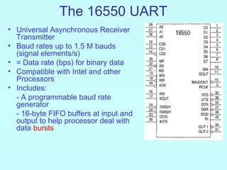
  • 1. The 16550 UART • Universal Asynchronous Receiver Transmitter • Baud rates up to 1.5 M bauds (signal elements/s) • = Data rate (bps) for binary data • Compatible with Intel and other Processors • Includes: - A programmable baud rate generator - 16-byte FIFO buffers at input and output to help processor deal with data bursts
  • 2. Asynchronous Serial Data Communication • Data sent asynchronously using the format illustrated below • We often use one start bit and one stop bit to frame the data, which is usually 8-data bits with or without parity Usually a byte of data
  • 3. The 16550 UART: Functional Description • Totally independent Transmitter (TX) and Receiver (RX) Sections • This allows communication in the following modes: - Simplex: Only TX or RX is used 40 pin DIP (one direction all the time) - Half Duplex: TX then RX (two directions at different times) - Full Duplex: TX and RX simultaneously (two directions at the same time) • Can control a modem using six signals, e.g. #DSR (Data Set Ready) input, #DTR (Data Terminal Ready) output…. Here the UART is the data terminal and modem is the dataset.
  • 4. The 16550 UART: Typical Configuration Serial to Parallel Or Parallel to Serial Converters Control µP 16-byte FIFO Input Buffer PS SIN Receiver UART Serial 16-byte FIFO Output Buffer PS Transmitter Comm. SOUT Link Data DMA Data Transfers: Memory  UART Directly Without going through the µP Memory
  • 5. The 16550 UART: Pin Assignments 3 I/O Address bits from Processor (Table 11-5) Chip Select Inputs Data bus to Processor (Multiple I/Ps) Master Reset (tie to µP Reset I/P) 40 pin DIP Read & Write Control inputs Serial data INput from RX from µP Serial data OUTput to TX (with complements for versatility Baud rate Clock output Address Strobe (not needed with Intels) Receiver Clock input Crystal or External Clock Input Modem Interface: TX ready for data. Put data into Inputs & Outputs UART by DMA Interrupt Processor User defined outputs RX ready with data. Take data from UART by DMA
  • 6. UARTs in the PC • Used to control the COM ports of the PC - UART at I/O address 3F8-3FF: COM Port 0 - UART at I/O address 2F8-2FF: COM Port 2
  • 7. Programming the UART Two Stages: a. Initialization Dialog: (Setup) - Follows RESET - Has two steps: 1. Program the line control register (Set asynchronous transmission parameters: # of stop, data, and parity bits, etc.) 2. Program the baud rate generator for the required baud rate b. Operation Dialog: (Actual Communication)
  • 8. The 8 I/O Byte Locations on the UART A2 A1 A0 Function 0 0 0 Receiver buffer (read data from RX) and transmitter holding (write data to TX). Also write LS byte of baud rate divisor 0 0 1 Interrupt enable. Also write MS byte of baud rate divisor 0 1 0 Interrupt identification (read) and FIFO control Register (write) - Used for operation dialog programming 0 1 1 Line control Register (Write into the line control register to program asynchronous communication at initialization) 1 0 0 Modem control 1 0 1 Line status LSTAT (Read the line status register to see if TX or RX are ready and to check for errors ) 1 1 0 Modem status 1 1 1 Scratch
  • 9. 1. Programming the Line Control Register a. Initialization I/O Address: A2 A1 A0 = 011 Dialog Programming Parity Control DL bit must be set See next slide Data Length = 5 bits before you can load the divisor Data Length > 5 bits for the baud generator See Table on next slide A break is a minimum of 2 frames of 0’s To allow programming The baud rate generator
  • 10. The 3 Parity Control Bits in the Line Control Register ST P PE Function 0 0 0 No parity 0 0 1 Odd parity 0 1 0 No parity 0 1 1 Even parity 1 0 0 Undefined 1 0 1 Send/receive 1 (send 1 in place of the parity bit) 1 1 0 Undefined 1 1 1 Send/receive 0 (send 0 in place of the parity bit)
  • 11. 2. Programming the Baud rate Generator • Baud rate is programmed by loading a 16-bit Baud Rate Divisor Value divisor for the crystal oscillator (or external input) 110 10,473 frequency into the I/O port addresses: 300 3840  {A2 A1 A0} = 000: LS Byte of divisor 1200 920  {A2 A1 A0} = 001: MS Byte of divisor 2400 480 4800 240 • Divisor value is determined by the Oscillator frequency and the baud rate required: 9600 120 19,200 60 Divisor = Oscillator frequency / (16 * Baud rate) 38,400 30 57,600 20 Table shows divisor values required for various 115,200 10 baud rates for osc frequency = 18.432 MHz
  • 13. ;Initialization dialog for Figure 11-45 ;Baud rate 9600, 7 bit data, odd parity, 1 stop bit LINE EQU 0F3H ; A2 A1 A0 = 011 for the Line Control Register LSB EQU 0F0H ; A2 A1 A0 = 000 for LSB of divisor MSB EQU 0F1H ; A2 A1 A0 = 001 for MSB of divisor FIFO EQU 0F2H ; A2 A1 A0 = 010 for the FIFO Control Register INIT PROC NEAR MOV AL,10001010B OUT LINE,AL ; Enable Baud rate programming See slide 108 ; program Baud 9600 ; Divisor = 120d (see Table on slide 110) MOV AL,120 ; LSB of divisor OUT LSB,AL MOV AL,0 ; MS Byte of divisor OUT MSB,AL MOV AL,00001010B ;program 7 bit data, odd Must write this OUT LINE,AL ;parity, 1 stop bit into FIFO Register ;(& disable baud rate programming?) to enable communication and operation dialog MOV AL,00000111B ;enable transmitter and receiver programming OUT FIFO,AL ;by writing into the FIFO control Reg. RET INIT ENDP
  • 14. 16550 FIFO Control Register (Write) I/O Address: A2 A1 A0 = 010 Required to enable 1 1 1 actual communication (Operation Dialog)
  • 15. b. Operation Dialog 16550 Line Status Register (LSTAT) Programming I/O Address: A2 A1 A0 = 101 Before reading data from receiver, ensure RX has data [DR (bit 1) = 1] Error status bits Any being 1 indicates An error Before writing data for transmission, Ensure TX is ready to take it [TH (bit 5) = 1]
  • 16. ;A procedure that transmits the byte in AH serially ;via the 16650 UART LSTAT EQU 0F5H ; The Line status register (LSTAT) (A2 A1 A0 = 101) DATA EQU 0F0H ; TX/RX Data Register at (A2 A1 A0 = 000) SEND PROC NEAR USES AX .REPEAT ;test the TH bit (bit 5) in to see if TX is available IN AL,LSTAT TEST AL,20H ;20H is the mask for the TH bit .UNTIL !ZERO? MOV AL,AH OUT DATA,AL ;send data to TX (LSTAT) RET SEND ENDP
  • 17. ; Procedure receives byte from UART into AL if no comm. error ; If error detected, it load Al with ‘?’ as an alert LSTAT EQU 0F5H ; The Line status register (LSTAT) (A2 A1 A0 = 101) DATA EQU 0F0H ; TX/RX Data Register at (A2 A1 A0 = 000) REVC PROC NEAR .REPEAT IN AL,LSTAT ;test DR bit TEST AL,1 .UNTIL !ZERO? TEST AL,0EH ;test for any error .IF ZERO? ;no error IN AL,DATA ;Read RX Data Register into AL .ELSE ;any error MOV AL,’?’ ;Put “?” in AL to indicate error .ENDIF RET RECV ENDP