Performance Analysis of Low Power, High Gain Operational Amplifier Using CMOS VLSI Design
•
0 likes•370 views

The operational amplifier is one of the most useful and important component of analog electronics. They are widely used in popular electronics. Their primary limitation is that they are not especially fast. The typical performance degrades rapidly for frequencies greater than about 1 MHz, although some models are designed specifically to handle higher frequencies. The primary use of op-amps in amplifier and related circuits is closely connected to the concept of negative feedback. The operational amplifier has high gain, high input impedance and low output impedance. Here the operational amplifier designed by using CMOS VLSI technology having low power consumption and high gain.

Recommended
Recommended
More Related Content
What's hot
What's hot (19)
Similar to Performance Analysis of Low Power, High Gain Operational Amplifier Using CMOS VLSI Design
Similar to Performance Analysis of Low Power, High Gain Operational Amplifier Using CMOS VLSI Design (20)
Recently uploaded
Recently uploaded (20)
Performance Analysis of Low Power, High Gain Operational Amplifier Using CMOS VLSI Design
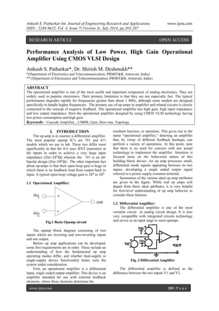
- 1. Ankush S. Patharkar Int. Journal of Engineering Research and Applications www.ijera.com ISSN : 2248-9622, Vol. 4, Issue 7( Version 3), July 2014, pp.203-207 www.ijera.com 203 | P a g e Performance Analysis of Low Power, High Gain Operational Amplifier Using CMOS VLSI Design Ankush S. Patharkar*, Dr. Shirish M. Deshmukh** *(Department of Electronics and Telecommunication, PRMIT&R, Amravati, India) ** (Department of Electronics and Telecommunication, PRMIT&R, Amravati, India) ABSTRACT The operational amplifier is one of the most useful and important component of analog electronics. They are widely used in popular electronics. Their primary limitation is that they are not especially fast. The typical performance degrades rapidly for frequencies greater than about 1 MHz, although some models are designed specifically to handle higher frequencies. The primary use of op-amps in amplifier and related circuits is closely connected to the concept of negative feedback. The operational amplifier has high gain, high input impedance and low output impedance. Here the operational amplifier designed by using CMOS VLSI technology having low power consumption and high gain. Keywords– Cascode Amplifier, , CMRR, Gain, Slew rate, Topology. I. INTRODUCTION The op-amp is in essence a differential amplifier. The most popular opamp IC's are 741 and 411 models which we use in lab. These two differ most significantly in that the 411 uses JFET transistors at the inputs in order to achieve a very large input impedance (Zin=109Ω) whereas the 741 is an all- bipolar design (Zin=106Ω) . The other important fact about op-amps is that their open-loop gain is huge in which there is no feedback loop from output back to input. A typical open-loop voltage gain is 104 to 105 1.1 Operational Amplifier: Fig.1 Basic Opamp circuit The opamp block diagram consisting of two inputs which are inverting and non-inverting inputs and one output. Before op amp applications can be developed, some first requirements are in order. These include an understanding of how the fundamental op amp operating modes differ, and whether dual-supply or single-supply device functionality better suits the system under consideration. First, an operational amplifier is a differential input, single ended output amplifier. This device is an amplifier intended for use with external feedback elements, where these elements determine the resultant function, or operation. This gives rise to the name "operational amplifier," denoting an amplifier that, by virtue of different feedback hookups, can perform a variety of operations. At this point, note that there is no need for concern with any actual technology to implement the amplifier. Attention is focused more on the behavioral nature of this building block device. An op amp processes small, differential mode signals appearing between its two inputs, developing a single ended output signal referred to a power supply common terminal. Summaries of the various ideal op amp attributes are given in the figure. While real op amps will depart from these ideal attributes, it is very helpful for first-level understanding of op amp behavior to consider these features. 1.2 Differential Amplifier: The differential amplifier is one of the most versatile circuit in analog circuit design. It is also very compatible with integrated circuits technology and serves as an input stage to most opamps. Fig. 2 Differential Amplifier The differential amplifier is defined as the difference between the two inputs V1 and V2. RESEARCH ARTICLE OPEN ACCESS
- 2. Ankush S. Patharkar Int. Journal of Engineering Research and Applications www.ijera.com ISSN : 2248-9622, Vol. 4, Issue 7( Version 3), July 2014, pp.203-207 www.ijera.com 204 | P a g e II. TWO STAGE DIFFERENTIAL AMPLIFIER Fig. 3 Two stage differential Amplifier The two stage amplifier consisting of single ended differential amplifier with high gain, second gain stage, biasing circuit and compensation circuit. The basic opamp architecture includes the high gain differential amplifier with dominant pole. The common source amplifier is used for second stage. The third stage is unity follower with a high frequency. The differential amplifier are usually used as a first stage in opamp with differential input and single ended output. The second stage increases the gain and also most desirable stage for high output swing. But as the gain increases this gives rise to lower the bandwidth and hence the designers had to decide between these tradeoffs. The purpose of the Compensation Circuit is to maintain stability when negative feedback is applied to the op amp. 1.3 Source coupled pair: The source-coupled pair comprised two MOS Ml and M2. When Ml and M2 are used in this configuration they are sometimes called a diff-pair. Fig. 4 Source coupled pair Since we know that a saturated MOSFET follows the relation The difference in the input voltages may be written as The maximum difference in the input voltages, maximum differential input voltage, is found by setting im to Iss (Ml conducting all of the tail bias current) and iD2 to 0 (M2 off) The minimum differential input voltage, 1.4 Folded cascode amplifier: The following figure shows the folded cascode amplifier Fig.5 Folded cascade Amplifier The folded cascode amplifier gives the same bias voltage at input and output. The typical gain value for this amplifier is 700 to 3000. The compensation is achieved by using load capacitor. As the load increases the opamp becomes slower but more stable. The cascode amplifier is used to drive the capacitor loads. III. PROPOSED ARCHITECTURE The proposed architecture consisting of bias circuit, differential input stage as the first stage, second stage as a common source stage, and the output buffer. Fig. 6 Proposed architecture of two stage amplifier The differential input stage as well as the common source stage consisting of PMOS and NMOS. The output buffer is used to drop capacitive loads. The differential and the common stage provide the high gain.
- 3. Ankush S. Patharkar Int. Journal of Engineering Research and Applications www.ijera.com ISSN : 2248-9622, Vol. 4, Issue 7( Version 3), July 2014, pp.203-207 www.ijera.com 205 | P a g e Fig.7 CMOS design of the stages 3.1 Op amp Gain: The gain of the opamp for the differential pair is, Gain of common source stage is, The gain of source follower is, 3.2 Small Signal opamp model: Fig.8 CMOS Design of stages Fig.9 Small signal model of opamp The transfer function can be given as, Assume widely separated poles, Dominant pole is, Non dominant pole is, As the value of 푔푚7 increases the pole distance also increases. The value of 퐶푐 may decrease the value of 푤푝1.
- 4. Ankush S. Patharkar Int. Journal of Engineering Research and Applications www.ijera.com ISSN : 2248-9622, Vol. 4, Issue 7( Version 3), July 2014, pp.203-207 www.ijera.com 206 | P a g e 3.3 Slew rate: Fig.10 CMOS design for slew rate calulation For large input signal the slew rate is given by The increase slew rate in two stage opamp can only be done by increasing unity gain frequency and increase in effective voltage in differential pair. The increase in unity gain frequency can be achieved by increase in 푤푝2 and keeping PM. IV. RESULTS The frequency responce for opamp is shown below. From the frequency respoce it is observed that the transconductance of the operational amplifier is 12 mA/V and the corresponding frequency is 79 MHz. The slew rate is defined as the rate of change of output with respect to time. The proposed operational amplifier has theoretical value of slew rate is 26 V/uS and the simulated slew rate value is 27.1 V/uS. Hence there is an improvement in the slew rate. Fig. 11 Frequency response of opamp From the above frequency responce we have, The slew rate is given by, Fig. 12 Slew rate calculation V. Conclusion The classical opamp have differential input stage, common source stage and optimal unity gain amplifier. The overall gain of the opamp is equal to product of stage gain. Here in this case the dominant pole is due to common source due to Miller effect. The second pole at the output can be increase by common source transconductance. The slew rate gives the maximum drive capability of output for large signals and may only be improved by increase in first stage effective voltage (gm1) or move second pole upwards. Compensation is done by pole splitting usually by exploring Miller capacitance. Differential amps have less common mode noise, but require additional common mode feedback circuit on output stage. Current mirror opamps are good and easy to use. References [1] R.J. Baker, H.W. Li, D.E. Boyce, CMOS circuit design layout and Simulation [2] P. E. Allen and D. R. Holberg, CMOS analog circuit design, 2nd edition [3] Roubik, G., "Introduction to CMOS op- amps and comparators", John Willy & Sons Inc, Vol. 189, (1999). [4] You Zheng and Carlos E. Saavedra, “Feedforward-Regulated Cascode OTA for
- 5. Ankush S. Patharkar Int. Journal of Engineering Research and Applications www.ijera.com ISSN : 2248-9622, Vol. 4, Issue 7( Version 3), July 2014, pp.203-207 www.ijera.com 207 | P a g e Gigahertz Applications “,IEEE Transactions on Circuits and Systems, 2008 [5] The International Technology Roadmap for Semiconductors (ITRS), 2006 [Online]. Available:http://www.itrs.net/Links/2006Update/2006UpdateFinal.htm [6] You, F., Embabi, S.H.K., Sanchez-Sinencio, E., "Multistage Amplifier Topologies with Nested Gm-C Compensation," IEEE Journal of Solid State Circuits, vol.32, no.12, Dec 1997. [7] Eschauzier, R.G.H., Huijsing, J.H., "A 100- MHz 100-dB operational amplifier with multipath Nested Miller compensation," IEEE Journal of Solid State Circuits, vol. 27, no. 12, pp. 1709-1716, Dec. 1992. [8] Leung, K. N., Mok, P. K. T., "Nested Miller compensation in low-power CMOS design," IEEE Transaction on Circuits and Systems II, Analog and Digital Signal Processing, vol. 48, no. 4, pp. 388-394, Apr. 2001. [9] Ferreira, L. H. C., Pimenta, T. C. and Moreno, R. L., "An ultralow-voltage ultra- low-power CMOS miller OTA with rail-to- rail input/output swing", IEEE Transactions on Circuits and Systems II: Express Briefs, Vol. 54, No. 10, (2007), 843-847.