Solid state device modeling and simulation jan2013 (1)
•
1 like•3,717 views

Recommended

Recommended
More Related Content
Similar to Solid state device modeling and simulation jan2013 (1)
Similar to Solid state device modeling and simulation jan2013 (1) (20)
More from SRI TECHNOLOGICAL SOLUTIONS
More from SRI TECHNOLOGICAL SOLUTIONS (20)
Solid state device modeling and simulation jan2013 (1)
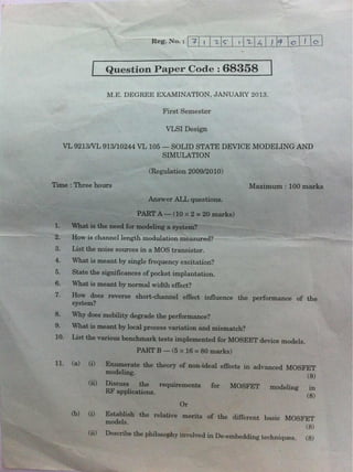
- 1. I Question Paper Code: 68358 I M.E. DEGREE EXAMINATION, JANUARY 2013. First Semester VLSI Design VL 9213NL 913/10244 VL 105 - SOLID STATE DEVICE MODELING AND SIMULATION (Regulation 2009/2010) Time : Three hours Maximum: 100 marks Answer ALL questions. PART A - (10 x 2 = 20 marks) 1. What is the need for modeling a system? 2. How is channel length modulation measured? 3. List the noise sources in a MOS transistor. 4. What is meant by single frequency excitation? 5. State the significances of pocket implantation. 6. What is meant by normal width effect? 7. How does reverse short-channel effect influence the performance of the system? 8. Why does mobility degrade the performance? 9. What is meant by local process variation and mismatch? 10. List the various benchmark tests implemented for MOSEET device models. PART B - (5 x 16 = 80 marks) II. (a) (i) Enumerate the theory of non-ideal effects in advanced MOSFET modeling. (8) (ii) Discuss the' requirements for MOSFET modeling In RF applications. (8) Or (b) (i) Establish the relative merits of the different basic MOSFET models. (8) (ii) Describe the philosophy involved in De-embedding techniques. (8)