SlideShare a Scribd company logo
1 of 6
Download to read offline
Post Graduate Diploma in IC Layout Design


Eligibility:
BE/ B.Tech/ MSc. in Electronics/ Electronics & Telecommunication/
Instrumentation/ Electrical/ Computers/ Information Technology/ MCA/ MCS/
AMIE /AMIETE or equivalent.


 Course No.                          Title                       Credits
                            Semester I (Six Months)

 ELICD-101       Foundation Course in Analog VLSI Design    5 (T) + 5 (P)
 ELICD-102       Foundation Course in Digital VLSI Design   5 (T) + 5 (P)
 ELICD-103       Foundation course in CMOS                  5 (T)
 ELICD-104       Foundation course IC Layout Design         5 (T) + 5 (P)
 ELICD-105       Foundation course in IPR Management        5 (T)

                           Semester II (Four Months)

 ELICD-201       Project                                    10
                           T- Theory, P- Practicals
ELICD-101: Foundation Course in Analog VLSI Design                      Credits: 5 (T) + 5 (P)

PN Junction, CMOS Transistors, Simple MOS Large Signal Model, Small-signal MOS Model,
Analog Subcircuits, MOS Switch, MOS and Bipolar Current Source/Sinks, Current Mirrors,
Basic principles of analog IC design -Matching, Process and temperature variations,

Introduction to feedback circuits, Loop gain, Reference circuits and voltage regulators, Current
and Voltage References, Bandgap Voltage References, Operational Transconductance
Amplifiers, General Design Principles of Op Amps, Op-amp application circuits and op-amp
characteristics, Transistor-level view of a two-stage op-amp, Output stages, Device high-
frequency small-signal models & capacitances, Simplified BW and high-frequency analysis, BW
limitations of basic gain stages: common-source and cascode amplifiers, Slew-rate and BW
limitations of op-amps, Frequency-response and stability of feedback circuits, Phase and gain
margins, Frequency compensation techniques, Cascode Op Amps,

Digital-Analog & Analog-Digital Converters, Analog and mixed devices and circuits, Analog
and mixed circuit design strategies and design optimizations, Circuit simulation tools like
Cadence, Mentor Graphics, PSPICE, testing and verification, Analog Circuit Modeling

Reference/Text Books

1. P. Gray, P. Hurst, S. Lewis, R. Meyer, "Analysis & Design of Analog Integrated Circuits,"
    WILEY
2. P. Allen, D. Holberg, "CMOS Analog Circuit Design, Second Edition," Oxford
3. D. Johns, K. Martin, "Analog Integrated Circuit Design," Wiley
4. B. Razavi, “Design of Analog CMOS Integrated Circuits” McGraw Hill
5. Sedra, Smith, "Microelectronics Circuits," 4th Edition, Oxford.
6. R. Jacob Baker , CMOS Mixed-Signal Circuit Design, Wiley
7. Ron Kielkowski, Inside SPICE, McGraw-Hill
8. Daniel Foty, MOSFET Modeling with SPICE, Prentice Hall
9. Yannis P. Tsividis, Operation and Modeling of the MOS Transistor, McGraw-Hill
10. Gordon W. Roberts and Adel S. Sedra, SPICE, Oxford University
11. R,V d Plassche “CMOS Analog to Digital and Digital to Analog Converters” Kluwer
    International
ELICD-102: Foundation Course in Digital VLSI Design                      Credits: 5 (T) + 5 (P)

CMOS inverter, characteristics, shift register, Flipflops, other basic cells, case studies, FPGA
Design Flow, ASIC Design Flow, Fault Modeling and Simulation CAD VLSI tools, simulators
for logic, timing, circuit, device and process optimization, Xilinx, Cadence, Mentor Graphics
simulation tools, Hardware description languages for VLSI design, VHDL and Verilog,

Combinatorial logic circuits and Sequential Ciruits, Arithmetic and Logic circuits, Comparison
circuits, adder, subtraction, look ahead carry, binary multiplication and division, floating and
fixed point arithmetic, ALU design, Finite state machines, Control Unit design

Hierarchical design methods Timing Analysis, Setup, Hold Times, Clock skew, Design
Tradeoffs: Designing for speed, power, reliability, testability, Power Analysis, Area and Power
Dissipation Estimation, Simultaneously switching outputs, VDD/VSS pairs, Ground Bounce,
Latch up, Metastability, Design for Testability, Fault Tolerance, Noise considerations for digital
IC’s

Reference/Text Books

1.   Rabaey, Chandrakasan, and Nikolic, Digital Integrated Circuits, A Design Perspective
2.   Weste and Harris CMOS VLSI Design
3.   Baker CMOS: Circuit Design, Layout and Simulation.
4.   Uyemura, CMOS Logic Circuit Design,
5.   Jaeger, Microelectronic Circuit Design
ELICD-103: Foundation Course in CMOS                                    Credits: 5 (T)
Introduction To CMOS Processes : Basic Processing Steps (Doping, Photolithography, Etching,
Deposition), PN Junction, MOS Transistors, MOS Device Design Equations, Electrical
Interaction Of Layers, NMOS And PMOS Cross Section And Operation, Technology
Considerations, Diode, BJT, MOS, Characteristics, models, CMOS Inverter Cross Section,
CMOS inverter DC, AC Analysis, Design tradeoffs, Introductions to CAD tools, Hierarchical
design of VLSIs, interception levels, behavioral description, RTL, Logic circuit, gate, circuits,
device and process. Properties of silicon wafers: Mechanical, Electrical, structural, Si wafer
growth techniques

Epitaxial growth, Oxidation, Diffusion, theory of diffusion, Ion implantation, ion implantation
system and principles, Metallization: Deposition techniques, Etching: Etch mechanisms,

The cost -volume trade-off, role of design center and foundry, design methodologies, custom and
semicustom designs, standard cell, gate array, FPGA, CPLD and PLDs, FPGA Design Flow,
ASIC Design Flow, IC design methodology and terminology, IC Packaging and Bonding
techniques, Physics of Power Dissipation in a nanometer CMOS, Design of Low Voltage
CMOS Circuits, Low Power SRAM Architectures, Power Estimation/Analysis Techniques,
Power Optimization Techniques Adaptive Power Supply Systems, Emerging Technologies,


Reference/Text Books
1. N. H. E. Weste and K. Eshraghian, Principles of CMOS VLSI Design, Addison-Wesley
2. Wayne Wolf, Modern VLSI Design System – on – Chip Design, Pearson Education
3. M. Michael Vai, VLSI Design, CRC Press
4. J. P. Uyemura, CMOS Logic Circuit Design, Springer (Kluwer Academic Publishers)
5. Ken Martin, Digital Integrated Circuit Design, Oxford University Press
6. David Hodges, Horace G Jackson & Resve A Saleh, Analysis and design of Digital
   Integrated Circuits in Deep Submission Technology,
ELICD-104: Foundation Course in IC Layout Design                        Credits: 5 (T) + 5 (P)


Layout techniques on devices: CMOS transistors, bipolar transistors, resistors, capacitors, and
diodes, Transistors in series and parallel. Finger & Bend gates, Stick diagrams, Transistor,
Schematic, logic & Complex logic fundamentals, Resistance and Capacitance theories and
calculations in layout. Theories on Parasitic R&C, Analog circuit and device matching theories,
Simple Static CMOS Gates, Inverting And Non-Inverting Gates, CMOS Inverter, Complex
Static CMOS Gates, Special CMOS Gates, Pull Up To Pull Down Ratio, Correspondence Of
Design Parameters With Specifications, Switching Characteristics, Transistor Sizing, Power
Dissipation, Design Margining, Scaling Of Device Dimensions, CMOS Logic Gate Design,
Mask Layout Designs For NMOS/CMOS, NAND, NOR Gates, 2 Input Multiplexer, Layout
Optimization For Performance, Clocking Strategies, Clock circuit & Clock Skew issues, Lamda
based design rules

Concepts of analog layout-Sharing, Fingering, Matching, Shielding & crosstalk, Second order &
Short channel effects, Issues to take care in analog layout- Latch up, Antenna effect, Electro
migration, Electrostatic discharge, Antenna issue, Latch up theory & prevention, High Voltage
circuit theory, I/O circuit, Noise and ground bounce theories, Strapping and Guard-ring
techniques, Advanced Digital and Analog mixed-signal layout techniques, High speed layout
techniques, High Voltage layout techniques, Reverse Engineering techniques, ESD and
Peripheral output driver and I/O cell layout techniques. Placement and routing techniques, Chip
floor planning techniques, Bonding pad, Seal-ring, Scribe-line layout techniques, Power bus
routing, bus slotting, and Clock net routing techniques. Extracting Circuits From Layout, Split
Gates, Cell Layout, Schematic And Layout Transistor Densities. Mixed Signal Circuits and
Layouts: Nonlinear Analog Circuits, Dynamic Analog Circuits, Data Converter Fundamentals,
DAC and ADC.

Introduction to Cadence virtuoso-Basic commands, Bind keys, Layout related functions, Layout
vs layout, Layout design & verification-Floor planning- hierarchical design, Power planning, Pin
placement, Understanding Design rules, DRC / LVS with ASSURA, Assignments- P - cells
creation, Simple inverter, D – flip flop, Custom digital layout, Current mirrors/ buffers/
differential pair, Two stage differential amplifier, High current switches, Resistor/Capacitor
dividers, “Layout design & verification of LDO”.

Reference/Text Books
   1. A. Hastings “The Art of Analog Layout” Prentice Hall
   2. Baker, Li Boyce, CMOS Circuit Design , Layout and Simulation
   3. C. Saint “IC Mask Design” McGraw Hill
   4. M.J.S.Smith, Application Specific Integrated Circuits, Addison-Wesley
   5. S. Kang and Yusuf Leblebici,
6. CMOS Digital Integrated Circuits Analysis and Design, McGraw-Hill
   7. H. E. Weste and David Harris, Principles of CMOS VLSI Design, Addison Wesley
   8. Dan Clein, Newnes, CMOS IC Layout,


ELICD-105: Foundation Course in IPR Management                             Credits: 5 (T)

Knowledge, Innovation and Intellectual Property Rights: An Introduction, Knowledge –
characteristics and role in economic growth, Tacit and codified knowledge, Knowledge as public
good and ‘market failure’, Market for knowledge, Incentives for creation of new knowledge,
Appropriation of knowledge: knowledge monopoly and its consequences, Pre-IPR system of
protection: Secrecy/Trade guilds/Cartels, IPR: Consequentiality, right based justification and
economic justification, Evolution of IP Statutes – Origin and Internationalization, International
organizations and Treaties (pre- TRIPs era): Paris Convention, Berne Convention, Rome
convention, IPIC Treaty, Budapest Treaty. CBD, UPOV convention. WIPO, GATT, FAO,
UNCTAD, Basic forms of IPRs: Patent, copyright, trademark, industrial design, Patents and
Patent information, Need for Patent, Patentable and Non-Patentable Invention, Types of Patent
application in India, PCT System, Guidelines for Registration of Patent, Patent filing, Opposition
and Grant, Concept of design, Design Act 2000, Need for protection of design, Concept,
Purpose, Characteristics and functions of Trademark, Copyright and Geographical Indications,
Concept of Copyright, Works Protected and Not Protected by Copyright, Copyright in Digital
era, Concept of Geographical Indications, IP Management, IPR Audit, Range and Classification
of IP Services

IPR Regime, Principles of IP Management, Sectoral IPR Debates on IPR and Development, IPRs
and technology transfer, IPRs vis-à-vis access & affordability of medicines, Traditional
knowledge, IPR and Benefit sharing, Indigenous knowledge and its appropriation, IPR in
Semiconductor IC Layout Design, Concept of Integrated Circuit Layout design, Registration of
Integrated Circuit Layout design, Semiconductor Chip Protection Copyrights, design registration,
design protection, licensing, IP reuse.

Reference/Text Books
1. Deborah E. Bouchoux Intellectual Property for Paralegals Cengage Learning
2. Prabuddha Ganguli Intellectual Property Rights Tata McGraw Hill
3. R. Radhakrishnan, S. Balasubramanian Intellectual Property Rights : Text and
   Cases Excel Books
4. Richard Stim Intellectual Property: Patents, Trademarks and Copyrights Cengage
   Learning


ELICD – 201 : Project


An extensive project involving either Layout design of complete VLSI or an exhaustive analysis
of the obtained Layout design from the point of view of IP protection/infringement.

More Related Content

Similar to 7 pg diploma ic layout design

syllbus (2).docx
syllbus (2).docxsyllbus (2).docx
syllbus (2).docxashwkr07
 
Ec6601 vlsi design syllabus for 6 th sem ece regulation 2013 anna universit...
Ec6601 vlsi design syllabus for 6 th sem ece regulation 2013   anna universit...Ec6601 vlsi design syllabus for 6 th sem ece regulation 2013   anna universit...
Ec6601 vlsi design syllabus for 6 th sem ece regulation 2013 anna universit...Raja Posupo
 
IES_Syllabus_for_Electronics.pdf colour based product sorting
IES_Syllabus_for_Electronics.pdf colour based product sortingIES_Syllabus_for_Electronics.pdf colour based product sorting
IES_Syllabus_for_Electronics.pdf colour based product sortingsanthoshmaha001
 
William Check Resume
William Check ResumeWilliam Check Resume
William Check ResumeBill Check
 
Copy of entc be syllabus
Copy of entc be syllabusCopy of entc be syllabus
Copy of entc be syllabusAmir Wagdarikar
 
2.ME VLSI 233-251.doc
2.ME VLSI 233-251.doc2.ME VLSI 233-251.doc
2.ME VLSI 233-251.docSRI NISHITH
 
2013 regulation syllabus for m.e vlsi design
2013 regulation syllabus for m.e vlsi design2013 regulation syllabus for m.e vlsi design
2013 regulation syllabus for m.e vlsi designkalaimathi mathiyazhagan
 
Gate syllabus
Gate syllabusGate syllabus
Gate syllabusRaj Kumar
 
Digital systems computer_electronics
Digital systems  computer_electronicsDigital systems  computer_electronics
Digital systems computer_electronicsNeeharika Kasarla
 
Digital systems computer_electronics
Digital systems  computer_electronicsDigital systems  computer_electronics
Digital systems computer_electronicsNeeharika Kasarla
 
EC(UVCE) 6th sem syllabus copy form lohith kumar 11guee6018
EC(UVCE) 6th sem syllabus copy form lohith kumar 11guee6018EC(UVCE) 6th sem syllabus copy form lohith kumar 11guee6018
EC(UVCE) 6th sem syllabus copy form lohith kumar 11guee6018UVCE
 
3rd year syllabus electronics & communication 2018 19
3rd year syllabus electronics & communication 2018 193rd year syllabus electronics & communication 2018 19
3rd year syllabus electronics & communication 2018 19kkmpec
 

Similar to 7 pg diploma ic layout design (20)

syllbus (2).docx
syllbus (2).docxsyllbus (2).docx
syllbus (2).docx
 
M Tech New Syllabus(2012)
M Tech New Syllabus(2012)M Tech New Syllabus(2012)
M Tech New Syllabus(2012)
 
Ec6601 vlsi design syllabus for 6 th sem ece regulation 2013 anna universit...
Ec6601 vlsi design syllabus for 6 th sem ece regulation 2013   anna universit...Ec6601 vlsi design syllabus for 6 th sem ece regulation 2013   anna universit...
Ec6601 vlsi design syllabus for 6 th sem ece regulation 2013 anna universit...
 
Ekt
EktEkt
Ekt
 
CMOS-IC Design NOTES Lodhi.pdf
CMOS-IC Design NOTES Lodhi.pdfCMOS-IC Design NOTES Lodhi.pdf
CMOS-IC Design NOTES Lodhi.pdf
 
ASHFAQUR_RAHMAN_Resume
ASHFAQUR_RAHMAN_ResumeASHFAQUR_RAHMAN_Resume
ASHFAQUR_RAHMAN_Resume
 
IES_Syllabus_for_Electronics.pdf colour based product sorting
IES_Syllabus_for_Electronics.pdf colour based product sortingIES_Syllabus_for_Electronics.pdf colour based product sorting
IES_Syllabus_for_Electronics.pdf colour based product sorting
 
William Check Resume
William Check ResumeWilliam Check Resume
William Check Resume
 
Copy of entc be syllabus
Copy of entc be syllabusCopy of entc be syllabus
Copy of entc be syllabus
 
2.ME VLSI 233-251.doc
2.ME VLSI 233-251.doc2.ME VLSI 233-251.doc
2.ME VLSI 233-251.doc
 
2013 regulation syllabus for m.e vlsi design
2013 regulation syllabus for m.e vlsi design2013 regulation syllabus for m.e vlsi design
2013 regulation syllabus for m.e vlsi design
 
Gate syllabus
Gate syllabusGate syllabus
Gate syllabus
 
vlsi
vlsivlsi
vlsi
 
Digital systems computer_electronics
Digital systems  computer_electronicsDigital systems  computer_electronics
Digital systems computer_electronics
 
Digital systems computer_electronics
Digital systems  computer_electronicsDigital systems  computer_electronics
Digital systems computer_electronics
 
Gagan_Resume
Gagan_ResumeGagan_Resume
Gagan_Resume
 
EC(UVCE) 6th sem syllabus copy form lohith kumar 11guee6018
EC(UVCE) 6th sem syllabus copy form lohith kumar 11guee6018EC(UVCE) 6th sem syllabus copy form lohith kumar 11guee6018
EC(UVCE) 6th sem syllabus copy form lohith kumar 11guee6018
 
3rd year syllabus electronics & communication 2018 19
3rd year syllabus electronics & communication 2018 193rd year syllabus electronics & communication 2018 19
3rd year syllabus electronics & communication 2018 19
 
Resume
ResumeResume
Resume
 
CAB
CABCAB
CAB
 

Recently uploaded

VIP Call Girls Service Bhagyanagar Hyderabad Call +91-8250192130
VIP Call Girls Service Bhagyanagar Hyderabad Call +91-8250192130VIP Call Girls Service Bhagyanagar Hyderabad Call +91-8250192130
VIP Call Girls Service Bhagyanagar Hyderabad Call +91-8250192130Suhani Kapoor
 
Best VIP Call Girls Noida Sector 47 Call Me: 8448380779
Best VIP Call Girls Noida Sector 47 Call Me: 8448380779Best VIP Call Girls Noida Sector 47 Call Me: 8448380779
Best VIP Call Girls Noida Sector 47 Call Me: 8448380779Delhi Call girls
 
VIP Call Girls Service Kukatpally Hyderabad Call +91-8250192130
VIP Call Girls Service Kukatpally Hyderabad Call +91-8250192130VIP Call Girls Service Kukatpally Hyderabad Call +91-8250192130
VIP Call Girls Service Kukatpally Hyderabad Call +91-8250192130Suhani Kapoor
 
WAEC Carpentry and Joinery Past Questions
WAEC Carpentry and Joinery Past QuestionsWAEC Carpentry and Joinery Past Questions
WAEC Carpentry and Joinery Past QuestionsCharles Obaleagbon
 
The history of music videos a level presentation
The history of music videos a level presentationThe history of music videos a level presentation
The history of music videos a level presentationamedia6
 
Verified Trusted Call Girls Adugodi💘 9352852248 Good Looking standard Profil...
Verified Trusted Call Girls Adugodi💘 9352852248  Good Looking standard Profil...Verified Trusted Call Girls Adugodi💘 9352852248  Good Looking standard Profil...
Verified Trusted Call Girls Adugodi💘 9352852248 Good Looking standard Profil...kumaririma588
 
CALL ON ➥8923113531 🔝Call Girls Aminabad Lucknow best Night Fun service
CALL ON ➥8923113531 🔝Call Girls Aminabad Lucknow best Night Fun serviceCALL ON ➥8923113531 🔝Call Girls Aminabad Lucknow best Night Fun service
CALL ON ➥8923113531 🔝Call Girls Aminabad Lucknow best Night Fun serviceanilsa9823
 
Cheap Rate ➥8448380779 ▻Call Girls In Huda City Centre Gurgaon
Cheap Rate ➥8448380779 ▻Call Girls In Huda City Centre GurgaonCheap Rate ➥8448380779 ▻Call Girls In Huda City Centre Gurgaon
Cheap Rate ➥8448380779 ▻Call Girls In Huda City Centre GurgaonDelhi Call girls
 
VIP College Call Girls Gorakhpur Bhavna 8250192130 Independent Escort Service...
VIP College Call Girls Gorakhpur Bhavna 8250192130 Independent Escort Service...VIP College Call Girls Gorakhpur Bhavna 8250192130 Independent Escort Service...
VIP College Call Girls Gorakhpur Bhavna 8250192130 Independent Escort Service...Suhani Kapoor
 
Cheap Rate Call girls Kalkaji 9205541914 shot 1500 night
Cheap Rate Call girls Kalkaji 9205541914 shot 1500 nightCheap Rate Call girls Kalkaji 9205541914 shot 1500 night
Cheap Rate Call girls Kalkaji 9205541914 shot 1500 nightDelhi Call girls
 
VIP Call Girl Amravati Aashi 8250192130 Independent Escort Service Amravati
VIP Call Girl Amravati Aashi 8250192130 Independent Escort Service AmravatiVIP Call Girl Amravati Aashi 8250192130 Independent Escort Service Amravati
VIP Call Girl Amravati Aashi 8250192130 Independent Escort Service AmravatiSuhani Kapoor
 
DragonBall PowerPoint Template for demo.pptx
DragonBall PowerPoint Template for demo.pptxDragonBall PowerPoint Template for demo.pptx
DragonBall PowerPoint Template for demo.pptxmirandajeremy200221
 
Cosumer Willingness to Pay for Sustainable Bricks
Cosumer Willingness to Pay for Sustainable BricksCosumer Willingness to Pay for Sustainable Bricks
Cosumer Willingness to Pay for Sustainable Bricksabhishekparmar618
 
Kindergarten Assessment Questions Via LessonUp
Kindergarten Assessment Questions Via LessonUpKindergarten Assessment Questions Via LessonUp
Kindergarten Assessment Questions Via LessonUpmainac1
 
Best VIP Call Girls Noida Sector 44 Call Me: 8448380779
Best VIP Call Girls Noida Sector 44 Call Me: 8448380779Best VIP Call Girls Noida Sector 44 Call Me: 8448380779
Best VIP Call Girls Noida Sector 44 Call Me: 8448380779Delhi Call girls
 
Kala jadu for love marriage | Real amil baba | Famous amil baba | kala jadu n...
Kala jadu for love marriage | Real amil baba | Famous amil baba | kala jadu n...Kala jadu for love marriage | Real amil baba | Famous amil baba | kala jadu n...
Kala jadu for love marriage | Real amil baba | Famous amil baba | kala jadu n...babafaisel
 

Recently uploaded (20)

VIP Call Girls Service Bhagyanagar Hyderabad Call +91-8250192130
VIP Call Girls Service Bhagyanagar Hyderabad Call +91-8250192130VIP Call Girls Service Bhagyanagar Hyderabad Call +91-8250192130
VIP Call Girls Service Bhagyanagar Hyderabad Call +91-8250192130
 
Best VIP Call Girls Noida Sector 47 Call Me: 8448380779
Best VIP Call Girls Noida Sector 47 Call Me: 8448380779Best VIP Call Girls Noida Sector 47 Call Me: 8448380779
Best VIP Call Girls Noida Sector 47 Call Me: 8448380779
 
VIP Call Girls Service Kukatpally Hyderabad Call +91-8250192130
VIP Call Girls Service Kukatpally Hyderabad Call +91-8250192130VIP Call Girls Service Kukatpally Hyderabad Call +91-8250192130
VIP Call Girls Service Kukatpally Hyderabad Call +91-8250192130
 
escort service sasti (*~Call Girls in Prasad Nagar Metro❤️9953056974
escort service sasti (*~Call Girls in Prasad Nagar Metro❤️9953056974escort service sasti (*~Call Girls in Prasad Nagar Metro❤️9953056974
escort service sasti (*~Call Girls in Prasad Nagar Metro❤️9953056974
 
WAEC Carpentry and Joinery Past Questions
WAEC Carpentry and Joinery Past QuestionsWAEC Carpentry and Joinery Past Questions
WAEC Carpentry and Joinery Past Questions
 
young call girls in Pandav nagar 🔝 9953056974 🔝 Delhi escort Service
young call girls in Pandav nagar 🔝 9953056974 🔝 Delhi escort Serviceyoung call girls in Pandav nagar 🔝 9953056974 🔝 Delhi escort Service
young call girls in Pandav nagar 🔝 9953056974 🔝 Delhi escort Service
 
The history of music videos a level presentation
The history of music videos a level presentationThe history of music videos a level presentation
The history of music videos a level presentation
 
Verified Trusted Call Girls Adugodi💘 9352852248 Good Looking standard Profil...
Verified Trusted Call Girls Adugodi💘 9352852248  Good Looking standard Profil...Verified Trusted Call Girls Adugodi💘 9352852248  Good Looking standard Profil...
Verified Trusted Call Girls Adugodi💘 9352852248 Good Looking standard Profil...
 
CALL ON ➥8923113531 🔝Call Girls Aminabad Lucknow best Night Fun service
CALL ON ➥8923113531 🔝Call Girls Aminabad Lucknow best Night Fun serviceCALL ON ➥8923113531 🔝Call Girls Aminabad Lucknow best Night Fun service
CALL ON ➥8923113531 🔝Call Girls Aminabad Lucknow best Night Fun service
 
Cheap Rate ➥8448380779 ▻Call Girls In Huda City Centre Gurgaon
Cheap Rate ➥8448380779 ▻Call Girls In Huda City Centre GurgaonCheap Rate ➥8448380779 ▻Call Girls In Huda City Centre Gurgaon
Cheap Rate ➥8448380779 ▻Call Girls In Huda City Centre Gurgaon
 
VIP College Call Girls Gorakhpur Bhavna 8250192130 Independent Escort Service...
VIP College Call Girls Gorakhpur Bhavna 8250192130 Independent Escort Service...VIP College Call Girls Gorakhpur Bhavna 8250192130 Independent Escort Service...
VIP College Call Girls Gorakhpur Bhavna 8250192130 Independent Escort Service...
 
Cheap Rate Call girls Kalkaji 9205541914 shot 1500 night
Cheap Rate Call girls Kalkaji 9205541914 shot 1500 nightCheap Rate Call girls Kalkaji 9205541914 shot 1500 night
Cheap Rate Call girls Kalkaji 9205541914 shot 1500 night
 
VIP Call Girl Amravati Aashi 8250192130 Independent Escort Service Amravati
VIP Call Girl Amravati Aashi 8250192130 Independent Escort Service AmravatiVIP Call Girl Amravati Aashi 8250192130 Independent Escort Service Amravati
VIP Call Girl Amravati Aashi 8250192130 Independent Escort Service Amravati
 
B. Smith. (Architectural Portfolio.).pdf
B. Smith. (Architectural Portfolio.).pdfB. Smith. (Architectural Portfolio.).pdf
B. Smith. (Architectural Portfolio.).pdf
 
DragonBall PowerPoint Template for demo.pptx
DragonBall PowerPoint Template for demo.pptxDragonBall PowerPoint Template for demo.pptx
DragonBall PowerPoint Template for demo.pptx
 
Call Girls Service Mukherjee Nagar @9999965857 Delhi 🫦 No Advance VVIP 🍎 SER...
Call Girls Service Mukherjee Nagar @9999965857 Delhi 🫦 No Advance  VVIP 🍎 SER...Call Girls Service Mukherjee Nagar @9999965857 Delhi 🫦 No Advance  VVIP 🍎 SER...
Call Girls Service Mukherjee Nagar @9999965857 Delhi 🫦 No Advance VVIP 🍎 SER...
 
Cosumer Willingness to Pay for Sustainable Bricks
Cosumer Willingness to Pay for Sustainable BricksCosumer Willingness to Pay for Sustainable Bricks
Cosumer Willingness to Pay for Sustainable Bricks
 
Kindergarten Assessment Questions Via LessonUp
Kindergarten Assessment Questions Via LessonUpKindergarten Assessment Questions Via LessonUp
Kindergarten Assessment Questions Via LessonUp
 
Best VIP Call Girls Noida Sector 44 Call Me: 8448380779
Best VIP Call Girls Noida Sector 44 Call Me: 8448380779Best VIP Call Girls Noida Sector 44 Call Me: 8448380779
Best VIP Call Girls Noida Sector 44 Call Me: 8448380779
 
Kala jadu for love marriage | Real amil baba | Famous amil baba | kala jadu n...
Kala jadu for love marriage | Real amil baba | Famous amil baba | kala jadu n...Kala jadu for love marriage | Real amil baba | Famous amil baba | kala jadu n...
Kala jadu for love marriage | Real amil baba | Famous amil baba | kala jadu n...
 

7 pg diploma ic layout design

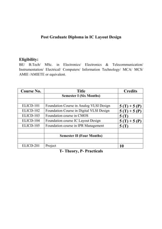
  • 1. Post Graduate Diploma in IC Layout Design Eligibility: BE/ B.Tech/ MSc. in Electronics/ Electronics & Telecommunication/ Instrumentation/ Electrical/ Computers/ Information Technology/ MCA/ MCS/ AMIE /AMIETE or equivalent. Course No. Title Credits Semester I (Six Months) ELICD-101 Foundation Course in Analog VLSI Design 5 (T) + 5 (P) ELICD-102 Foundation Course in Digital VLSI Design 5 (T) + 5 (P) ELICD-103 Foundation course in CMOS 5 (T) ELICD-104 Foundation course IC Layout Design 5 (T) + 5 (P) ELICD-105 Foundation course in IPR Management 5 (T) Semester II (Four Months) ELICD-201 Project 10 T- Theory, P- Practicals
  • 2. ELICD-101: Foundation Course in Analog VLSI Design Credits: 5 (T) + 5 (P) PN Junction, CMOS Transistors, Simple MOS Large Signal Model, Small-signal MOS Model, Analog Subcircuits, MOS Switch, MOS and Bipolar Current Source/Sinks, Current Mirrors, Basic principles of analog IC design -Matching, Process and temperature variations, Introduction to feedback circuits, Loop gain, Reference circuits and voltage regulators, Current and Voltage References, Bandgap Voltage References, Operational Transconductance Amplifiers, General Design Principles of Op Amps, Op-amp application circuits and op-amp characteristics, Transistor-level view of a two-stage op-amp, Output stages, Device high- frequency small-signal models & capacitances, Simplified BW and high-frequency analysis, BW limitations of basic gain stages: common-source and cascode amplifiers, Slew-rate and BW limitations of op-amps, Frequency-response and stability of feedback circuits, Phase and gain margins, Frequency compensation techniques, Cascode Op Amps, Digital-Analog & Analog-Digital Converters, Analog and mixed devices and circuits, Analog and mixed circuit design strategies and design optimizations, Circuit simulation tools like Cadence, Mentor Graphics, PSPICE, testing and verification, Analog Circuit Modeling Reference/Text Books 1. P. Gray, P. Hurst, S. Lewis, R. Meyer, "Analysis & Design of Analog Integrated Circuits," WILEY 2. P. Allen, D. Holberg, "CMOS Analog Circuit Design, Second Edition," Oxford 3. D. Johns, K. Martin, "Analog Integrated Circuit Design," Wiley 4. B. Razavi, “Design of Analog CMOS Integrated Circuits” McGraw Hill 5. Sedra, Smith, "Microelectronics Circuits," 4th Edition, Oxford. 6. R. Jacob Baker , CMOS Mixed-Signal Circuit Design, Wiley 7. Ron Kielkowski, Inside SPICE, McGraw-Hill 8. Daniel Foty, MOSFET Modeling with SPICE, Prentice Hall 9. Yannis P. Tsividis, Operation and Modeling of the MOS Transistor, McGraw-Hill 10. Gordon W. Roberts and Adel S. Sedra, SPICE, Oxford University 11. R,V d Plassche “CMOS Analog to Digital and Digital to Analog Converters” Kluwer International
  • 3. ELICD-102: Foundation Course in Digital VLSI Design Credits: 5 (T) + 5 (P) CMOS inverter, characteristics, shift register, Flipflops, other basic cells, case studies, FPGA Design Flow, ASIC Design Flow, Fault Modeling and Simulation CAD VLSI tools, simulators for logic, timing, circuit, device and process optimization, Xilinx, Cadence, Mentor Graphics simulation tools, Hardware description languages for VLSI design, VHDL and Verilog, Combinatorial logic circuits and Sequential Ciruits, Arithmetic and Logic circuits, Comparison circuits, adder, subtraction, look ahead carry, binary multiplication and division, floating and fixed point arithmetic, ALU design, Finite state machines, Control Unit design Hierarchical design methods Timing Analysis, Setup, Hold Times, Clock skew, Design Tradeoffs: Designing for speed, power, reliability, testability, Power Analysis, Area and Power Dissipation Estimation, Simultaneously switching outputs, VDD/VSS pairs, Ground Bounce, Latch up, Metastability, Design for Testability, Fault Tolerance, Noise considerations for digital IC’s Reference/Text Books 1. Rabaey, Chandrakasan, and Nikolic, Digital Integrated Circuits, A Design Perspective 2. Weste and Harris CMOS VLSI Design 3. Baker CMOS: Circuit Design, Layout and Simulation. 4. Uyemura, CMOS Logic Circuit Design, 5. Jaeger, Microelectronic Circuit Design
  • 4. ELICD-103: Foundation Course in CMOS Credits: 5 (T) Introduction To CMOS Processes : Basic Processing Steps (Doping, Photolithography, Etching, Deposition), PN Junction, MOS Transistors, MOS Device Design Equations, Electrical Interaction Of Layers, NMOS And PMOS Cross Section And Operation, Technology Considerations, Diode, BJT, MOS, Characteristics, models, CMOS Inverter Cross Section, CMOS inverter DC, AC Analysis, Design tradeoffs, Introductions to CAD tools, Hierarchical design of VLSIs, interception levels, behavioral description, RTL, Logic circuit, gate, circuits, device and process. Properties of silicon wafers: Mechanical, Electrical, structural, Si wafer growth techniques Epitaxial growth, Oxidation, Diffusion, theory of diffusion, Ion implantation, ion implantation system and principles, Metallization: Deposition techniques, Etching: Etch mechanisms, The cost -volume trade-off, role of design center and foundry, design methodologies, custom and semicustom designs, standard cell, gate array, FPGA, CPLD and PLDs, FPGA Design Flow, ASIC Design Flow, IC design methodology and terminology, IC Packaging and Bonding techniques, Physics of Power Dissipation in a nanometer CMOS, Design of Low Voltage CMOS Circuits, Low Power SRAM Architectures, Power Estimation/Analysis Techniques, Power Optimization Techniques Adaptive Power Supply Systems, Emerging Technologies, Reference/Text Books 1. N. H. E. Weste and K. Eshraghian, Principles of CMOS VLSI Design, Addison-Wesley 2. Wayne Wolf, Modern VLSI Design System – on – Chip Design, Pearson Education 3. M. Michael Vai, VLSI Design, CRC Press 4. J. P. Uyemura, CMOS Logic Circuit Design, Springer (Kluwer Academic Publishers) 5. Ken Martin, Digital Integrated Circuit Design, Oxford University Press 6. David Hodges, Horace G Jackson & Resve A Saleh, Analysis and design of Digital Integrated Circuits in Deep Submission Technology,
  • 5. ELICD-104: Foundation Course in IC Layout Design Credits: 5 (T) + 5 (P) Layout techniques on devices: CMOS transistors, bipolar transistors, resistors, capacitors, and diodes, Transistors in series and parallel. Finger & Bend gates, Stick diagrams, Transistor, Schematic, logic & Complex logic fundamentals, Resistance and Capacitance theories and calculations in layout. Theories on Parasitic R&C, Analog circuit and device matching theories, Simple Static CMOS Gates, Inverting And Non-Inverting Gates, CMOS Inverter, Complex Static CMOS Gates, Special CMOS Gates, Pull Up To Pull Down Ratio, Correspondence Of Design Parameters With Specifications, Switching Characteristics, Transistor Sizing, Power Dissipation, Design Margining, Scaling Of Device Dimensions, CMOS Logic Gate Design, Mask Layout Designs For NMOS/CMOS, NAND, NOR Gates, 2 Input Multiplexer, Layout Optimization For Performance, Clocking Strategies, Clock circuit & Clock Skew issues, Lamda based design rules Concepts of analog layout-Sharing, Fingering, Matching, Shielding & crosstalk, Second order & Short channel effects, Issues to take care in analog layout- Latch up, Antenna effect, Electro migration, Electrostatic discharge, Antenna issue, Latch up theory & prevention, High Voltage circuit theory, I/O circuit, Noise and ground bounce theories, Strapping and Guard-ring techniques, Advanced Digital and Analog mixed-signal layout techniques, High speed layout techniques, High Voltage layout techniques, Reverse Engineering techniques, ESD and Peripheral output driver and I/O cell layout techniques. Placement and routing techniques, Chip floor planning techniques, Bonding pad, Seal-ring, Scribe-line layout techniques, Power bus routing, bus slotting, and Clock net routing techniques. Extracting Circuits From Layout, Split Gates, Cell Layout, Schematic And Layout Transistor Densities. Mixed Signal Circuits and Layouts: Nonlinear Analog Circuits, Dynamic Analog Circuits, Data Converter Fundamentals, DAC and ADC. Introduction to Cadence virtuoso-Basic commands, Bind keys, Layout related functions, Layout vs layout, Layout design & verification-Floor planning- hierarchical design, Power planning, Pin placement, Understanding Design rules, DRC / LVS with ASSURA, Assignments- P - cells creation, Simple inverter, D – flip flop, Custom digital layout, Current mirrors/ buffers/ differential pair, Two stage differential amplifier, High current switches, Resistor/Capacitor dividers, “Layout design & verification of LDO”. Reference/Text Books 1. A. Hastings “The Art of Analog Layout” Prentice Hall 2. Baker, Li Boyce, CMOS Circuit Design , Layout and Simulation 3. C. Saint “IC Mask Design” McGraw Hill 4. M.J.S.Smith, Application Specific Integrated Circuits, Addison-Wesley 5. S. Kang and Yusuf Leblebici,
  • 6. 6. CMOS Digital Integrated Circuits Analysis and Design, McGraw-Hill 7. H. E. Weste and David Harris, Principles of CMOS VLSI Design, Addison Wesley 8. Dan Clein, Newnes, CMOS IC Layout, ELICD-105: Foundation Course in IPR Management Credits: 5 (T) Knowledge, Innovation and Intellectual Property Rights: An Introduction, Knowledge – characteristics and role in economic growth, Tacit and codified knowledge, Knowledge as public good and ‘market failure’, Market for knowledge, Incentives for creation of new knowledge, Appropriation of knowledge: knowledge monopoly and its consequences, Pre-IPR system of protection: Secrecy/Trade guilds/Cartels, IPR: Consequentiality, right based justification and economic justification, Evolution of IP Statutes – Origin and Internationalization, International organizations and Treaties (pre- TRIPs era): Paris Convention, Berne Convention, Rome convention, IPIC Treaty, Budapest Treaty. CBD, UPOV convention. WIPO, GATT, FAO, UNCTAD, Basic forms of IPRs: Patent, copyright, trademark, industrial design, Patents and Patent information, Need for Patent, Patentable and Non-Patentable Invention, Types of Patent application in India, PCT System, Guidelines for Registration of Patent, Patent filing, Opposition and Grant, Concept of design, Design Act 2000, Need for protection of design, Concept, Purpose, Characteristics and functions of Trademark, Copyright and Geographical Indications, Concept of Copyright, Works Protected and Not Protected by Copyright, Copyright in Digital era, Concept of Geographical Indications, IP Management, IPR Audit, Range and Classification of IP Services IPR Regime, Principles of IP Management, Sectoral IPR Debates on IPR and Development, IPRs and technology transfer, IPRs vis-à-vis access & affordability of medicines, Traditional knowledge, IPR and Benefit sharing, Indigenous knowledge and its appropriation, IPR in Semiconductor IC Layout Design, Concept of Integrated Circuit Layout design, Registration of Integrated Circuit Layout design, Semiconductor Chip Protection Copyrights, design registration, design protection, licensing, IP reuse. Reference/Text Books 1. Deborah E. Bouchoux Intellectual Property for Paralegals Cengage Learning 2. Prabuddha Ganguli Intellectual Property Rights Tata McGraw Hill 3. R. Radhakrishnan, S. Balasubramanian Intellectual Property Rights : Text and Cases Excel Books 4. Richard Stim Intellectual Property: Patents, Trademarks and Copyrights Cengage Learning ELICD – 201 : Project An extensive project involving either Layout design of complete VLSI or an exhaustive analysis of the obtained Layout design from the point of view of IP protection/infringement.