Modulador de Ancho de Pulso en Fuentes ATX Sdc7500
•
0 j'aime•4,437 vues

Utilizado en Fuentes ATX de PC

Recommandé
Contenu connexe
Tendances
Tendances (20)
Similaire à Modulador de Ancho de Pulso en Fuentes ATX Sdc7500
Similaire à Modulador de Ancho de Pulso en Fuentes ATX Sdc7500 (20)
Plus de Juan Carlos Ruiz
Dernier
Dernier (20)
Modulador de Ancho de Pulso en Fuentes ATX Sdc7500
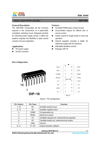
- 1. Data sheet January,2010 Rev1.0 1/7 ○C 2012 Shaoxing Devechip Microelectronics Co.,Ltd www.sdc-semi.com Voltage Mode PWM Controller SDC7500 General Description The SDC7500 incorporates all the functions required in the construction of a pulse-width modulation switching circuit. Designed primarily for switching power supply control, it offers the systems engineer the flexibility to tailor control circuitry to its own application. Applications PC power supply DC-DC convertor Features Complete PWM power control circuitry Uncommitted outputs for 200mA sink or source current Output control for single ended or push pull operation Internal regulator provides a stable 5V reference supply with 5% tolerance Adjustable deadtime control Package: DIP-16 Pin Configuration Figure 1. Pin Configuration Pin Number Pin Name Function 1, 16 IN+ Amplifier positive input 2, 15 IN- Amplifier negative input 3 COMP Compensation pin 4 DEAD Dead time control 5 CT Oscillate capacitor pin, external timing capacitor 6 RT Oscillate resistor pin, external timing resistor 7 GND Ground 8, 11 C1, C2 Output transistor collector
- 2. Data sheet January,2010 Rev1.0 2/7 ○C 2012 Shaoxing Devechip Microelectronics Co.,Ltd www.sdc-semi.com Voltage Mode PWM Controller SDC7500 9,10 E1, E2 Output transistor emitter 12 VCC Power supply pin 13 CTRL Output control pin 14 VREF Reference pin Table 1. Pin Configuration Functional Block Diagram Figure 2. Functional Block Diagram Absolute Maximum Ratings(NOTE:Stresses greater than those listed under Absolute Maximum Ratings may cause permanent damage to the device.) Parameter Symbol Value Unit Power Supply Voltage VCC Vcc 42 V Amplifier Input Voltage Vi VCC+0.3 V Collector Output Voltage Vo 42 V Collector Output Current Ico 200 mA Total Dissipation power PD 1000 mW Operating Temperature Topr -25~85 ℃ Storage Temperature Tstg -65~150 ℃ Table 2. Absolute Maximum Ratings
- 3. Data sheet January,2010 Rev1.0 3/7 ○C 2012 Shaoxing Devechip Microelectronics Co.,Ltd www.sdc-semi.com Voltage Mode PWM Controller SDC7500 Electrical Characteristics(Vcc=15.0V, f=1KHz, Ta=25℃, unless otherwise specified.) Parameter Symbol Conditions Min Typ Max Unit REFERENCE SECTION Output Voltage Vref Iref=1mA 4.90 5.00 5.10 V Input Regulation Delta_VV VCC=7V~40V 2 25 mV Output Regulation Delta_VL Iref=1mA~10mA 1 15 mV Short-circuit Output Current Isc Vref=0V,Ta=25℃ 55 mA Output Voltage Change with Temperature Delta_VT ΔTA=MIN TO MAX 0.2 1 % PWM SECTION Input Threshold Voltage Vth DUTY=0 4 4.5 V Input Sink Current Isink VPIN3=0.7V 0.3 0.7 mA OSCILLATOR SECTION Frequency Fosc CT=1nF RT=12KΩ 23 29 34 KHz Standard Deviation of Frequency Delta ALL Value of CT RT TA constant 10 % Frequency Change with Temperature Delta_FT TA=MIN TO MAX 12 % Frequency Change with Voltage Delta_FV VCC=7V~40V 0.1 % AMPLIFIER SECTION Input Offset Voltage Voffset Vo(PIN3)=2.5V 2 10 mV Input Offset Current Ioffset Vo(PIN3)=2.5V 25 250 nA Input Bias Current Ibias Vo(PIN3)=2.5V 0.2 1 uA Output Sink Current Isink VCOMP=0.5V 0.3 0.7 mA Output Source Current Isourse VCOMP=3.5V -2 mA Common-mode Input Voltage Range VI VCC=7V~40V -0.3~VCC V Open-loop Voltage Amplification GV ΔVo=0.5V~3.5V 70 95 dB Unity-gain Bandwidth Fband 800 KHz Common-mode Rejection Ratio Rrej VCC=40V 65 80 dB DEAD TIME CONTROL SECTION Input Bias Ibias VI=0~5.25V -2 -10 uA Maximum Duty Cycle Gv VI(PIN4)=0 45 % Input Threshold Voltage Vth DUTY=0 2.7 3.3 V Input Threshold Voltage Vth DUTY=MAX 0 POWER CURRENT SECTION Standby Supply Current ICC1 VCC=15V 6 10 mA Standby Supply Current ICC VCC=40V 9 15 mA Average Supply Current Iav VPIN4=2V 7.5 mA
- 4. Data sheet January,2010 Rev1.0 4/7 ○C 2012 Shaoxing Devechip Microelectronics Co.,Ltd www.sdc-semi.com Voltage Mode PWM Controller SDC7500 OUTPUT SECTION Collector off-state Current IC VCE=40V VCC=40V 2 100 uA Emitter off-state Current IE VCC=VC=40V VE=0 -100 uA Common-emitter Vsat VE=0,IC=100mA 1.0 1.3 V Collector-emitter Saturation Voltage Emitter-follower Vsat VC=15V IE=-100mA 1.5 2.5 V Output Control Input Current Ii VI=Vref 3.5 mA SWITCHING CHARACTERISTICS Output Voltage Rise Time Tr 100 200 ns Output Voltage Fall Time Tf Common-emitter configuration 25 100 ns Output Voltage Rise Time Tr 100 200 ns Output Voltage Fall Time Tf Emitter-follower configuration 40 100 ns Table 3. Electrical Characteristics Typical Performance Characteristics Figure 3. oscillator frequency and frequency Figure4. amplifier voltage amplification variation VS timing resistance
- 5. Data sheet January,2010 Rev1.0 5/7 Voltage Mode PWM Controller SDC7500 Typical Application 12345678910111213141516+ VO+ + VO+ VO- VIN+ VIN- COMPDEADCTRTGNDC1E1E2C2VCCCTRLVREFVIN- VIN+ + VIN Figure 5. Typical Application ○C 2012 Shaoxing Devechip Microelectronics Co.,Ltd www.sdc-semi.com
- 6. Data sheet January,2010 Rev1.0 6/7 Voltage Mode PWM Controller SDC7500 Package Dimension ○C 2012 Shaoxing Devechip Microelectronics Co.,Ltd www.sdc-semi.com
- 7. Data sheet January,2010 Rev1.0 7/7 ○C 2012 Shaoxing Devechip Microelectronics Co.,Ltd www.sdc-semi.com Voltage Mode PWM Controller SDC7500 Shaoxing Devechip Microelectronics Co.,Ltd http://www.sdc-semi.com/ IMPORTANT NOTICE Information in this document is provided solely in connection with SDC products. SDC reserves the right to make changes, corrections, modifications or improvements, to this document, and the products and services described herein at anytime, without notice. Shaoxing Devechip Microelectronics Co.,Ltd does not assume any responsibility for use of any its products for any particular purpose, nor does Shaoxing Devechip Microelectronics Co.,Ltd assume any liability arising out of the application or use of any its products or circuits. Shaoxing Devechip Microelectronics Co.,Ltd does not convey any license under its patent rights or other rights nor the rights of others. © 2012 Devechip Microelectronics - All rights reserved Contact us: Headquarters of Shaoxing Shenzhen Branch Address:, Tian Mu Road, No13 Address: 22A Shangbu building, Nan Yuan Road, NO.68 Easter City, Shaoxing, Zhengjiang,.China Futian District, Shenzhen Zip code:312000 Zip code:518031 Tel:(86) 0575-8861 6750 Tel:(86) 0755-8366 1155 Fax:(86) 0575-8862 2882 Fax:(86) 0755-8301 8528