
Recommandé
Recommandé
Contenu connexe
Tendances
Tendances (18)
Similaire à Low Power 32×32 bit Multiplier Architecture based on Vedic Mathematics Using Virtex 7 Low Power Device
Similaire à Low Power 32×32 bit Multiplier Architecture based on Vedic Mathematics Using Virtex 7 Low Power Device (20)
Plus de VIT-AP University
Plus de VIT-AP University (20)
Dernier
Dernier (20)
Low Power 32×32 bit Multiplier Architecture based on Vedic Mathematics Using Virtex 7 Low Power Device
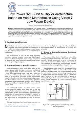
- 1. IJRREST INTERNATIONAL JOURNAL OF RESEARCH REVIEW IN ENGINEERING SCIENCE & TECHNOLOGY (ISSN 2278–6643) VOLUME-2, ISSUE-2, JUNE-2013 IJRREST, ijrrest.org 34 | P a g e Low Power 32×32 bit Multiplier Architecture based on Vedic Mathematics Using Virtex 7 Low Power Device *Neeraj Kumar Mishra, **Subodh Wairya Abstract— In this paper the most significant aspect of the proposed method is that, the developed multiplier architecture is based on vertical and crosswise structure of Ancient Indian Vedic Mathematics. As per this proposed architecture, for two 32-bit numbers; the multiplier and multiplicand, each are grouped as 16-bit numbers so that it decomposes into 16×16 multiplication modules. It is also illustrated that the further hierarchical decomposition of 8×8 modules into 4×4 modules and then 2×2 modules will have a significant VHDL coding of for 32x32 bits multiplication and their used FPGA family Virtex 7 low power implementation by Xilinx Synthesis 16.1 tool done. The synthesis results show that the computation time for calculating the product of 32x32 bits is delay 29.256 ns. (11.499ns logic, 11.994ns route) (48.9% logic, 51.1% route). —————————— —————————— 1 INTRODUCTION TO MULTIPLIER ultiplication is a crucial unfussy, basic function in arithmetic procedures and Vedic mathematics is a endowment prearranged for the paramount of human race, due to the capability it bestows for quicker intellectual computation. So multiplication is one of the most important operations in digital computer systems and digital signal processors. Beside multiplier is power hungry components so reducing their power dissipation satisfying the overall power budget of digital computer. 2 LITERATURE SURVEY OF VEDIC MATHEMATICS Vedic mathematics - a gift given to this world by the ancient sages of India. A system which is far simpler and more enjoyable than modern mathematics. The word “Vedic” is derived from the word “Veda” which means the store-house of all knowledge. Vedic mathematics is mainly based on 16 Sutras (or aphorisms) dealing with various branches of mathematics like arithmetic, algebra, geometry etc. These methods and ideas can be directly applied to trigonometry, plain and spherical geometry, conics, calculus (both differential and integral), and applied mathematics of various kinds. As mentioned earlier, all these Sutras were reconstructed from ancient Vedic texts early in the last century. Vedic mathematics requires no elucidation and enlightenment, for that reason we are not amplificating this algorithm in the manuscript, even though how the sutra is placed into maneuver in our work, is a matter of justification and is elucidated in the proposed multiplier architecture segment. In vedic mathematics there are 16 sutras use only one sutra to our multiplication algorithm that is Urdhva- tiryakbyham method of multiplication is Vertically and crosswise. 3 DETAILS OF URDHVA-TIRYAKBHHAM METHOD OF MULTIPLICATION The concept of the Urdhva-Tiryagbhyam sutra of the ancient Indian Vedic mathematics. It is based on a concept through which the generation of all partial products can be done with the concurrent addition of these partial products. The parallelism in generation of partial products and their summation is obtained using Urdhava Tiryakbhyam. Since the partial products and their sums are calculated in parallel, the multiplier is independent of the clock frequency of the processor. Thus the multiplier will require the same amount of time to calculate the product and hence is independent of the clock frequency. The net advantage is that it reduces the need of processors to operate at increasingly high clock frequencies. But this algorithm reduce power dissipation In Urdhva-Tiryagbhyam sutra algorithm discuss below Fig.1: Gate Level Diagram for Two Bit Using Urdhava Tiryakbhyam Sutra M ———————————————— *Dept. of ECE, R.D.F. Group of Institution Ghaziabad, U.P., India **Dept. of EC, IET Campus, Lucknow, U.P., India.
- 2. IJRREST INTERNATIONAL JOURNAL OF RESEARCH REVIEW IN ENGINEERING SCIENCE & TECHNOLOGY (ISSN 2278–6643) VOLUME-2, ISSUE-2, JUNE-2013 IJRREST, ijrrest.org 35 | P a g e 4 RELATED WORK OF 32×32 BIT VEDIC MULTIPLIER This paper is organized as follows: Section first describes Urdhva-Tiryagbhyam sutra, Section Second discusses the Design and implementation of 64bit multiplier, Section third Measure speed and delay of Xilinx Virtex 7 low power Device family, Last section Synthesis Report develop for speed grade -1 4.1 Design and Implementation of 32-bit Multiplier The Vedic multiplier is implemented using VHDL. In this multiplication algorithm chose two 32 bit these number are multiplied and give a 64 bit number for example consider two bit number these algorithm is as given below: Fig. 2: Two Bit Number Vedic Multiplication This algorithm is extended to further procedure for 4 bit number gives a 16bit output as shown below: Fig. 3: Four Bit Number Vedic Multiplication Now the procedure extended for 32bit multiplier gives 64bit output. Technique is used for multiplication is zero padding for example 4 bit number gives 8bit output as fig c right hand side bit called Lower side bit (LSB) and lest most bit called middle side bit (MSB) remaining bit are arrange in middle befor and after add a zero bit is called zero padding as shown in figure 4. arrange in the frame called zero padding. Above result for 4 bit number 0110 00011 0110 and 0011 MSB is left most bit 0110 and LSB is right most bit 0011 use a four signal called s1,s2,s3 and s4. Signal s1 is first horizontal line values is 0 1 1 0 0 0 0 0 signal s2 is second horizontal line value 0 0 0 0 0 0 1 1 signal s3 third horizontal line value is 0 0 0 0 1 1 0 0 and last signal s4 forth horizontal line value 0 0 0 1 1 0 0 0. We are here using a technique of zero padding and then as a final point an adder module if we are talking about 32×32 bit multiplier module then we will have to use four 32/2×32/2bit multiplier modules. Following the extremely comparable analogous approach we are proposing a 32 × 32 bit multiplier. The main projected structure for the 32×32 bit multiplier as fig 4. Fig. 4: Zero Padding Concept in 4 Bit Vedic Multiplier Now the generalized form for using signa s1,s2and s3 is shown below: Fig. 5: Generalized Architecture of Zero Padding Concept in 4 bit Vedic Multiplier 5 MEASURE SPEED AND DELAY XILINX VIRTEX 7 LOW POWER DEVICE FAMILY The proposed multiplier architecture is implemented in VHDL (Very High Speed Integrated Circuited Hardware Description Language) furthermore the FPGA device family Virtex 7 low power XC7V285TL, package FFG1925, speed grade -1L.Synthesis is done using Xilinx ISE Design Suite 13.1. The design is optimized for speed and delay using Xilinx13.1 found to be the most efficient in terms of both speed and delay Vedic multiplier code has been synthesized
- 3. IJRREST INTERNATIONAL JOURNAL OF RESEARCH REVIEW IN ENGINEERING SCIENCE & TECHNOLOGY (ISSN 2278–6643) VOLUME-2, ISSUE-2, JUNE-2013 IJRREST, ijrrest.org 36 | P a g e on XILINX FPGA. RTL schematic a test bench wave form found is shown in figure 6. Fig.6: RTL Schematic a Test Bench Fig.7: Hardware Architecture of Vedic 32-Bit Multiplier 6 SYNTHESIS REPORT DEVELOP FOR SPEED GRADE-1 The Vedic multiplier is implemented using VHDL and multipliers like Vedic multiplier of 32×32bit are implemented. The functional verification through simulation of the VHDL code was carried out using ModelSim simulator. The entire code is completely synthesizable. The synthesis is done using Xilinx Synthesis Tool (XST) available with Xilinx ISE 16.1. The design is optimized for speed and area using Xilinx, device family virtex 7 low power, and speed grade -1 is chosen. Table 1 and Table 2 indicate the device utilization summary of the array, and memory usage and delay of this particular device virtex 7 low power. Table 1 Table 2 CPU : 11.57 / 12.04 s | Elapsed : 11.00 / 12.00 s Total memory usage is 137824 kilobytes Macro Statistics for FPGA 32-bit / 4-inputs adder tree 64 Xors 8192 1-bit xor2 8192 delay 29.256 ns. (11.499ns logic, 11.994ns route) (48.9% logic, 51.1% route) 7 CONCLUSION The Vedic Mathematics gives us a clue of symmetric computation. Vedic mathematics deals with various topics of mathematics such as basic arithmetic, geometry, trigonometry, calculus etc. All these methods are very efficient as far as manual calculations are concerned. The proposed Vedic multiplier proves to be highly efficient in terms of the speed. The main advantage is delay increases slowly as the input bits increases total processing time depends upon the number used. The high speed multiplier algorithm exhibits improved efficiency in terms of speed and low power. REFERENCES Books: [1] F. Charles. Roth Jr. “Digital Systems Design using VHDL,” Thomson Brooks/Cole, 7th reprint, 2005. Logic Utilization Speed Used Available Utilization Number of Slices 1L 51030 178800 28% Number of bonded IOBs -1 512 1200 42%
- 4. IJRREST INTERNATIONAL JOURNAL OF RESEARCH REVIEW IN ENGINEERING SCIENCE & TECHNOLOGY (ISSN 2278–6643) VOLUME-2, ISSUE-2, JUNE-2013 IJRREST, ijrrest.org 37 | P a g e [2] Jagadguru Swami Sri Bharati Krisna Tirthaji Maharaja, Vedic Mathematics: Sixteen Simple Mathematical Formulae from the Veda, Delhi (1965). [3] Neil H.E Weste, David Harris, Ayan anerjee,”CMOS VLSI Design, A Circuits and Systems Perspective”,Third Edition, Published by Person Education, PP-327-328] Proceedings Papers: [4] Neeraj Mishra, Asmita Haveliya An advancement in the N×N Multiplier Architecture Realization via the Ancient Indian Vedic Mathematics, International Journal of Electronics Communication and Computer Engineering IJECCE Volume 4, Issue 2 [5] Ramalatha M, Thanushkodi K, Deena Dayalan K, Dharani P, A Novel Time and Energy Efficient Cubing Circuit using Vedic Mathematics for Finite Field Arithmetic, International Conference on Advances in Recent Technologies in Communication and Computing 2009. [6] Anvesh Kumar, Ashish Raman, Dr. R.K. Sarin, Dr. Arun Khosla, Small area Reconfigurable FFT Design by Vedic Mathematics, 2010 IEEE. [7] Honey Durga Tiwari, Ganzorig Gankhuyag, Chan Mo Kim, Yong Beom Cho, Multiplier design based on ancient Indian Vedic Mathematics, International SoC Design Conference 2008. [8] Sumita Vaidya and Deepak Dandekar, Delay-Power Performance comparison of Multipliers in VLSI Circuit Design, International Journal of Computer Networks & Communications (IJCNC), Vol.2, No.4, July 2010. [9] S.S. Kerur, Prakash Narchi, Jayashree C N, Harish M Kittur and Girish V A Implementation of Vedic Multiplier For Digital Signal Processing, International conference on VLSI communication & instrumentation (ICVCI) 2011. [10] S. Kumaravel, Ramalatha Marimuthu, "VLSI Implementation of High Performance RSA Algorithm Using Vedic Mathematics," ICCIMA, vol. 4,pp.126-128, International Conference on Computational Intelligence and Multimedia Applications (ICCIMA 2007), 2007. [11] N.-Y. Shen and O. T.-C. Chen, “Low-power multipliers by minimizing switching activities of partial products,” in Proc. IEEE Int. Symp. Circuits Syst., May 2002, vol. 4, pp. 93–96. [12] Shiann-Rong Kuang and Jiun-Ping Wang “Design of power efficient configurable booth multiplier” IEEE Trans. Circuits Syst. I Regular Papers vol. 57, no.3, pp. 568-580, March 2010 [13] T. Yamanaka and V. G. Moshnyaga, “Reducing energy of digital multiplier by adjusting voltage supply to multiplicand variation,” in Proc. 46th IEEE Midwest Symp. Circuits Syst., Dec. 2003, pp. 1423–1426.