![[object Object],[object Object],[object Object],[object Object],[object Object],Contents](data:image/gif;base64,R0lGODlhAQABAIAAAAAAAP///yH5BAEAAAAALAAAAAABAAEAAAIBRAA7)
Recommandé
Recommandé
Contenu connexe
Tendances
Tendances (20)
Similaire à Design Your Next Generation Product Using 3 D Lds Mid
Similaire à Design Your Next Generation Product Using 3 D Lds Mid (20)
Design Your Next Generation Product Using 3 D Lds Mid
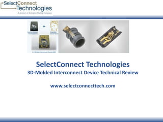
- 1. SelectConnect Technologies 3D-Molded Interconnect Device Technical Review www.selectconnecttech.com
- 3. 3D-Interconnects by DS / LDS Double-Shot Single-Shot LDS
- 4. LDS 3-D MID
- 5. LDS Summary
- 6. LDS Summary
- 12. LDS Pitch for High Yield 8 mil lines 10 mil spaces (18 mil pitch)
- 13. Business Drivers for 3D-MID Kavo Dental Tool
- 14. Business Drivers for 3D-MID Kavo Dental Tool
- 16. LDS Design Rules Siemans Hearing Aid Component
- 17. LDS Design Rules
- 18. LDS Design Rules
- 19. LDS Design Rules
- 21. LDS Design Rules
- 22. LDS Design Rules
- 23. Metallization Electroless Copper Nickel Immersion Gold [Electroless Gold] Typical builds: SelectConnect™ Metallization Copper 100 – 250 micro-inches (2.5 – 5.0 µm) Nickel 50 – 150 micro-inches (1.2 – 2.5 µm) Gold Immersion, ~ 8 micro-inches (0.2 µm)
- 24. Key Markets / Applications
- 25. Medical Devices OmniPod ® Insulin Management System OEM: Insulet Molder: Phillips Plastics Plater: Arlington Plating Material: PC, PC/ABS (doped) Process: DS (Double Shot)
- 28. Military / Defense Security Housing Manufacturer: Bourns Material: Pocan DP 7102 (PBT)
- 34. Automotive ASIC deposited onto MID with LPKF-LDS ® technology Conventional Solution Sensor ASIC MID using LPKF-LDS ® technology Source: Robert Bosch GmbH Rotation Sensor for Automotive Brake System (ESP) Flipped Positioned Signal Ground Support bumps
- 37. Automotive Former device Diameter approx. 10mm Prototype new Sensor Diameter: 5mm Realized by Flip Chip on LPKF-LDS ® MID Source: Robert Bosch GmbH Rotation Sensor for Automotive Brake System (ESP) Final Part
- 38. Automotive Source: ZMD AG AMR Sensor (Automotive) Material: Vectra E840i LDS
- 40. LED Lighting
- 42. Hundreds of millions of cell phone, tablet antennas produced annually LPKF-LDS ® antenna Cellular Electronics
- 44. LDS 3D-MID
- 45. Company Overview SelectConnect Technologies Division of Arlington Plating Company Palatine, Illinois
- 46. Company Overview Source Point Associates Brentwood, California 94513 Larry Megugorac 925.516.2082 Mobile 650 678 8987 [email_address] www. SourcePointAssociates.com LinkedIn: http://www.linkedin.com/in/larrymegugorac Twitter: @SourcePointAsso
Notes de l'éditeur
- Thank you for attending today’s webcast, a technical review on 3-D Molded Interconnect Devices
- This is a technical review for electrical and mechanical engineers and project managers involved in designing your next-generation products. We will cover the two processes for producing 3-dimensional molded interconnects; Double-Shot molding and Laser Direct Structuring, with an emphasis on laser direct structuring. We will briefly examine available LDS materials and the fundamental design rules for designing LDS 3D MID. And conclude with application examples employing 3-D MID, from the medical device, automotive, sensors, antenna and RFID fields.
- Three dimensional molded interconnect devices are a method to integrate electronic circuitry and electrical components with injection molded carriers. This process then is used on enclosures to miniaturize assemblies, reduce the bill of material, simplify designs, reduce assembly time and reduce costs of components/assemblies. The double-shot process is illustrated with the disposable insulin pump on the left, where circuitry is constructed by over-molding a plateable polycarbonate/ABS resin grade formed in the shape of the desired circuit, with a non-plateable polycarbonate material forming the chassis. The component is chemically etched and only the PC/ABS blended material is activated by the etchant. The plateable material is activated for plating using a palladium salt solution and the component is plated using an electroless process to complete the formation of the circuitry. The laser direct structuring method is illustrated in the part on the right. A laser is used to scribe circuit patterns onto a three-dimensional single-shot injection molded component. Both processes use an electroless plating process called the SelectConnect Process to metalize the circuit patterns, laying down a layer of electroless copper, electroless nickel, and finally, a layer of immersion gold or electrolytic gold for applications that require thicker layer of gold. It will focus on the LDS method of producing three-dimensional interconnects in this review.
- LDS 3D-MID are comprised of injection molded thermoplastic components overlaid with circuit traces drawn on the three-dimensional part using a laser marking system. The plastic components are made from material doped with organometallic micro-particles. The areas marked by the laser are activated and are plateable using electroless plating chemistry. The circuit traces are drawn on the three-dimensional CAD model as a zero-height surface. A .step file is exported from the CAD system for translation into laser coordinates. The pattern is aligned using optically detected fiducials located on the component or the laser table and the pattern is scanned onto the part using preprogrammed laser parameters appropriate for the type of material.
- The LDS process for producing 3-D MID is about 10 years old. It was developed in Germany by LPKF Laser and Electronics and for the first five or six years was a application looking for problem to solve. The first high volume application employing the LDS method for producing 3-D MID was in the area of cell phone antennas. Historically, antennas were modeled by hand, placing metal foil over forms and the antenna patterns were cut by hand using an Exact-O knife. The test piece was then placed in the RF range for evaluation. A new iteration of the antenna would require repeating this laborious process. Using the LDS process allows changes to be made to the drawing and accurately translated to parts in less time and with a higher degrees of accuracy.
- Today: LDS is a mature, robust technology Cell Phone Antenna production is largest application, with ten’s of millions produced annually Europe is currently experiencing rapid growth in automotive, with BMW taking the lead, medical devices, antennas systems, sensors and RF-ID tags
- The laser source is a 16W diode pumped Neodymium-doped yttrium orthovanadate (Nd:YVO 4 ) system operating in the near-infrared at 1064 nm with a focused spot size of 65µm. The system uses a high-speed scanner and optical z-axis for the 3D beam delivery with typical positioning speeds in the range of 1 to 4 meters per second. The laser’s interaction with the material surface is two-fold, the beam activates the surface by reducing the organometallic dopant to metal particles and it roughens up the surface providing a texture for mechanical adherence of the metalized layer.
- We often denote the laser’s impact on the material surface as a channel carved out of the material, but recent data for PC/ABS material shows just the opposite. The surface hit by the laser is roughened and raised in columnar fashion some 5 to 25 µm.
- Here is a profile of a circuit after plating.
- In a view from an variable pressure Scanning Electron Microscope (SEM), the surface topography is evident.
- In this SEM image a Back-Scattered Electron Detector highlights the metal catalyst additive appearing here as bright spots.
- LDS resolution of 6 mil lines and 8 mil spaces possible, with higher yields from 8 mil lines and 10 mil spaces. 4 mil lines and 6 mil spaces is possible on LCP material.
- Why pursue an LDS 3D-MID strategy? The LDS‘s market drivers are to Reduce: Reduce Size, weight and complexity of assemblies And to reduce Costs – through reduction in number of components, wires, interconnects and assembly time Benefits include improvement in: Reliability Functionality Here we see an example of a newly designed dental cavity detection system that uses LDS components. The new design features a completely self contained hand held laser caries detection system.
- The product has gone from a lunch pail sized electronics package with a tethered laser, to a self contained laser in a hand held device that communicates results wirelessly to a base station.
- A wide range of materials is available and qualified for LDS applications, from commodity materials through engineering resins with both amorphous and semi-crystalline characteristics. A family of high heat nylons, PET, PBT and blends are amenable to lead solder reflow mounting of components and LCP resins will perform with lead-free reflow solders. ====================================================== PET – Polyethylene Terephthalate PBT - Polybutylene Terephthalate PPA – Polyphthalamide PSU – Polysulfone PES – Polyethersulfone HTN – Polyamide PA6/6T- Nylons
- One of the important developments of 3-dimensional circuitry is the efficient use of space with the finest possible structures. When designing components for LDS production, one needs to keep a few basic design rules in mind.
- The areas to be laser activated must remain in the line of sight of the laser beam. The work zone of the laser is an area 160 x 160mm or approximately 6 square inches and the laser has a working distance of approximately 1 inch, which means the laser can focus on a part that has a Z range of height of 1 inch.
- It is possible to lase patterns on all sides of a part by designing a multi-position fixture or a fixture that can rotate parts for multiple passes.
- When positioning the parts in a fixture we have a maximum angle of incidence of the beam impinging on the part of 70 degrees. Angles of incidence exceeding 70° are reduced by rotating the component during laser processing.
- For parts with multiple surfaces with 90 degree angles, the part is mounted at an angle and is rotated to complete the activation.
- Plated through holes are activated using Conical Vias on one or both sides depending on part thickness. Thick walls require an aspect ratio of 2:1, while thinner parts can use simple cones with a 1:1 ratio.
- When designing molds, we must pay attention to the location of walls and ejection pins. Zones to be activated should not directly touch walls Activation area separation for walls with an angle up to 45° should be kept at >150 µm or 6 mil Steeper walls with angles up to about 70° should be separated by 250 µm or greater or 10 mil Ejector pins should be placed to avoid the activation areas
- The plating process consists of electroless plating chemistries, typically starting with a layer of 100 to 250 micro-inches of copper, followed by a 50 to 150 micro inch layer of nickel and an optional thin layer of immersion gold or a gold layer built using electroless gold chemistry that can build a more substantial gold layer. Metal thickness can be customized to meet the needs of the design.
- Let’s take a look at some application examples in the area of: Medical Devices Military / Defense / Aerospace Automotive Electronics Antennas RFID
- This is the Omni Pod from Insulet Corporation. It is a disposable insulin pump and blood glucose measurement system Advantages Disposable Communicates Wirelessly with the Handheld Provides mechanical support and electrical connectivity Smaller, lighter - Allows for integration of more electronic functions - Eliminates complicated assemblies
- In this example, Siemens developed an integrated approach to mounting components on a 3-dimensional carrier for their hearing aids.
- The Kavo dental caries detection tool Features: An LDS produced mode switch assembly that provided a: Reduction of assembly time from 20 seconds to 6 seconds Increase of assembly yield Reduction of the number of parts from 8 to 3 And a cost reduction of 78%
- Security Shields Are a injection molded enclosure with a layer of delicate and geometrically fine tracks covering the inside of the security housing. The tracks are less than 10 μm thick making it difficult to detect using X-rays. They are designed to protect against conducting and non-conducting drill bits and are resistant to chemical attack. Benefits over other solutions include: • It is simple to attach to the PCB • Fewer assembly steps • The elimination of epoxy potting • The design allows for recovery of PCB for repair, upgrade or data recovery • Housing can be removed without damaging the PCB • And it lends itself to automated assembly processes
- BMW motorcyles is employing a Multifunction Human Machine Interface, a switch assembly, That Features: A 14 function switch A reduction of size and weight The substitution of a wiring harness and PCB The Integration of connectors And a water tight assembly
- The switch assembly is assembled using 3D Pick and Place robots and reflow soldering
- One can get creative using LDS technology, here the part is tagged with a 3-dimensional scanner code for identification and tracability
- The automotive sector is embracing LDS produced 3D-MID for the reductions in cost, weight, assembly times and the resultant increase in reliability. The 2014 model year will feature integration in the area of: Switches in the dash and steering wheel Seat modules containing seat-occupied and seat belt sensors LED position lighting In-Door electronics modules
- This BMW prototype under development by TRW will integrate all steering wheel functions using surface mounted LEDs, electronics and switches.
- In this application, an Application Specific Integrated Circuit or ASIC, in a flip-chip format, is mounted to a single piece LDS produced MID carrier to produce a wheel rotation sensor.
- With a goal of increased reliability over a wide thermal cycling range
- And after 1,000 hours, 300 units experienced “zero” defects
- This shows the evolution of the part; highlighting size and weight reduction of the part from old to new.
- In this example an AMR, a form of magnetic field sensor and its associated electrical components are housed in an LDS created 3D-MID for: Increased functionality in reduced space Precise 3D orientation of the sensor chip Minimized assembly complexity Increase the ease of assembly Higher reliability ============================ (AMR stands for anisotropic magneto-resistance)
- LDS produced 3D-MID are increasingly being used to mount Application Specific Intergrated Circuits in carriers, providing a protective package and easy component integration. Here are two examples of pressure sensors MIDs.
- LDS produced 3D-MID are increasingly being used to mount Application Specific Intergrated Circuits in carriers, providing a protective package and easy component integration. Here are two examples of pressure sensors MIDs.
- LED lighting applications are moving into the consumer space in automotive, aircraft and sport lighting. Featuring a: Reduction of weight and size The Substitution of socket and lamp Longer life time with LED light sources Integrated cooling built using LDS metallization Adding up to a maintenance-free lighting system
- Hundreds of millions of LDS cell phone and tablet antennas are produced annually
- In the RFID space, LDS 3D-MID provide flexibility to rapidly produce and change - Antenna patterns for different frequencies and applications And integrated protection of the devices
- So LDS 3D-Molded Interconnect Devices are coming of age. It is a mature, cost effective, robust technology poised to expand into new markets that require efficient use of space, simpler assemblies and more reliable performance. Thank you for you time today. Please feel free to contact me with questions or to discuss a project.
- We are located in suburban Chicago. - SelectConnect Technologies Formed in 2009 as a division of Arlington Plating Company - To Manufacture 3D-MID (Molded Interconnect Devices) We developed the patented SelectConnect TM Plating Process for plating circuitry on plastic components using both the Laser Direct Structuring & Double Shot 3D-MID Processes