Strategies for Unlocking Knowledge Management in Microsoft 365 in the Copilot...
4057
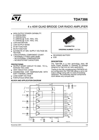
1. ® TDA7386
4 x 40W QUAD BRIDGE CAR RADIO AMPLIFIER
HIGH OUTPUT POWER CAPABILITY:
4 x 45W/4Ω MAX.
4 x 40W/4Ω EIAJ
4 x 28W/4Ω @ 14.4V, 1KHz, 10%
4 x 24W/4Ω @ 13.2V, 1KHz, 10%
LOW DISTORTION
LOW OUTPUT NOISE
ST-BY FUNCTION FLEXIWATT25
MUTE FUNCTION ORDERING NUMBER: TDA7386
AUTOMUTE AT MIN. SUPPLY VOLTAGE DE-
TECTION
LOW EXTERNAL COMPONENT COUNT: REVERSED BATTERY
– INTERNALLY FIXED GAIN (26dB) ESD
– NO EXTERNAL COMPENSATION
– NO BOOTSTRAP CAPACITORS
DESCRIPTION
PROTECTIONS: The TDA7386 is a new technology class AB
OUTPUT SHORT CIRCUIT TO GND, TO VS, Audio Power Amplifier in Flexiwatt 25 package
ACROSS THE LOAD designed for high end car radio applications.
VERY INDUCTIVE LOADS Thanks to the fully complementary PNP/NPN out-
put configuration the TDA7386 allows a rail to rail
OVERRATING CHIP TEMPERATURE WITH
output voltage swing with no need of bootstrap
SOFT THERMAL LIMITER capacitors. The extremely reduced components
LOAD DUMP VOLTAGE count allows very compact sets.
FORTUITOUS OPEN GND
BLOCK AND APPLICATION DIAGRAM
Vcc1 Vcc2
470µF 100nF
ST-BY
N.C.
MUTE
OUT1+
IN1 OUT1-
0.1µF PW-GND
OUT2+
IN2 OUT2-
0.1µF PW-GND
OUT3+
IN3 OUT3-
0.1µF PW-GND
OUT4+
IN4 OUT4-
0.1µF PW-GND
AC-GND SVR TAB S-GND
0.47µF 47µF
D99AU1018
November 2001 1/9
2. TDA7386
ABSOLUTE MAXIMUM RATINGS
Symbol Parameter Value Unit
VCC Operating Supply Voltage 18 V
VCC (DC) DC Supply Voltage 28 V
VCC (pk) Peak Supply Voltage (t = 50ms) 50 V
IO Output Peak Current:
Repetitive (Duty Cycle 10% at f = 10Hz) 4.5 A
Non Repetitive (t = 100µs) 5.5 A
Ptot Power dissipation, (Tcase = 70°C) 80 W
Tj Junction Temperature 150 °C
Tstg Storage Temperature – 55 to 150 °C
PIN CONNECTION (Top view)
1 25
TAB
P-GND2
OUT2-
ST-BY
OUT2+
VCC
OUT1-
P-GND1
OUT1+
SVR
IN1
IN2
S-GND
IN4
IN3
AC-GND
OUT3+
P-GND3
OUT3-
VCC
OUT4+
MUTE
OUT4-
P-GND4
HSD
D94AU159A
THERMAL DATA
Symbol Parameter Value Unit
Rth j-case Thermal Resistance Junction to Case Max. 1 °C/W
2/9
3. TDA7386
ELECTRICAL CHARACTERISTICS (VS = 14.4V; f = 1KHz; Rg = 600Ω; RL = 4Ω; Tamb = 25°C;
Refer to the test and application diagram, unless otherwise specified.)
Symbol Parameter Test Condition Min. Typ. Max. Unit
Iq1 Quiescent Current RL = ∞ 190 350 mA
VOS Output Offset Voltage Play Mode ±80 mV
dVOS During mute ON/OFF output ±80 mV
offset voltage
Gv Voltage Gain 25 26 27 dB
dGv Channel Gain Unbalance ±1 dB
Po Output Power VS = 13.2V; THD = 10% 22 24 W
VS = 13.2V; THD = 0.8% 16.5 18 W
VS = 14,4V; THD = 10% 26 28 W
Po EIAJ EIAJ Output Power (*) VS = 13.7V 37.5 40 W
Po max. Max. Output Power (*) VS = 14.4V 43 45 W
THD Distortion Po = 4W 0.04 0.15 %
eNo Output Noise "A" Weighted 50 70 µV
Bw = 20Hz to 20KHz 70 100 µV
SVR Supply Voltage Rejection f = 100Hz; Vr = 1Vrms 50 75 dB
fch High Cut-Off Frequency PO = 0.5W 80 200 KHz
Ri Input Impedance 70 100 KΩ
CT Cross Talk f = 1KHz PO = 4W 60 70 – dB
f = 10KHz PO = 4W 60 – dB
ISB St-By Current Consumption VSt-By = 1.5V 50 µA
Ipin4 St-by pin Current VSt-By = 1.5V to 3.5V ±10 µA
VSB out St-By Out Threshold Voltage (Amp: ON) 3.5 V
VSB in St-By in Threshold Voltage (Amp: OFF) 1.5 V
AM Mute Attenuation POref = 4W 80 90 dB
VM out Mute Out Threshold Voltage (Amp: Play) 3.5 V
VM in Mute In Threshold Voltage (Amp: Mute) 1.5 V
VAM in VS Automute Threshold (Amp: Mute)
Att ≥ 80dB; POref = 4W 6.5 V
(Amp: Play)
Att < 0.1dB; PO = 0.5W 7.6 8.5 V
Ipin22 Muting Pin Current VMUTE = 1.5V 5 11 20 µA
(Sourced Current)
VMUTE = 3.5V -5 20 µA
(*) Saturated square wave output.
3/9
5. TDA7386
Figure 2: P.C.B. and component layout of the figure 1 (1:1 scale)
COMPONENTS &
TOP COPPER LAYER
BOTTOM COPPER LAYER
5/9
6. TDA7386
Figure 3: Quiescent Current vs. Supply Voltage Figure 4: Quiescent Output Voltage vs. Supply
Voltage
Figure 5: Output Power vs. Supply Voltage Figure 6: Maximum Output Power vs. Supply
Voltage
Figure 7: Distortion vs. Output Power Figure 8: Distortion vs. Frequency
6/9
7. TDA7386
Figure 9: Supply Voltage Rejection vs. Figure 10: Crosstalk vs. Frequency
Frequency
Figure 11: Output Noise vs. Source Resistance Figure 12: Power Dissipation & Efficiency vs.
Output Power
APPLICATION HINTS (ref. to the circuit of fig. 1) CMOS-COMPATIBLE. If unused, a straight con-
SVR nection to Vs of their respective pins would be ad-
missible. Conventional/low-power transistors can
Besides its contribution to the ripple rejection, the be employed to drive muting and stand-by pins in
SVR capacitor governs the turn ON/OFF time se- absence of true CMOS ports or microprocessors.
quence and, consequently, plays an essential role
in the pop optimization during ON/OFF tran- R-C cells have always to be used in order to
sients.To conveniently serve both needs, ITS smooth down the transitions for preventing any
MINIMUM RECOMMENDED VALUE IS 10µF. audible transient noises.
Since a DC current of about 10 uA normally flows
out of pin 22, the maximum allowable muting-se-
INPUT STAGE ries resistance (R2) is 70KΩ, which is sufficiently
The TDA7386’s inputs are ground-compatible and high to permit a muting capacitor reasonably
can stand very high input signals (± 8Vpk) without small (about 1µF).
any performances degradation. If R2 is higher than recommended, the involved
If the standard value for the input capacitors risk will be that the voltage at pin 22 may rise to
(0.1µF) is adopted, the low frequency cut-off will above the 1.5 V threshold voltage and the device
amount to 16 Hz. will consequently fail to turn OFF when the mute
line is brought down.
STAND-BY AND MUTING About the stand-by, the time constant to be as-
signed in order to obtain a virtually pop-free tran-
STAND-BY and MUTING facilities are both sition has to be slower than 2.5V/ms.
7/9
8. TDA7386
mm inch
DIM.
MIN. TYP. MAX. MIN. TYP. MAX.
A 4.45 4.50 4.65 0.175 0.177 0.183 OUTLINE AND
B 1.80 1.90 2.00 0.070 0.074 0.079 MECHANICAL DATA
C 1.40 0.055
D 0.75 0.90 1.05 0.029 0.035 0.041
E 0.37 0.39 0.42 0.014 0.015 0.016
F (1) 0.57 0.022
G 0.80 1.00 1.20 0.031 0.040 0.047
G1 23.75 24.00 24.25 0.935 0.945 0.955
H (2) 28.90 29.23 29.30 1.138 1.150 1.153
H1 17.00 0.669
H2 12.80 0.503
H3 0.80 0.031
L (2) 22.07 22.47 22.87 0.869 0.884 0.904
L1 18.57 18.97 19.37 0.731 0.747 0.762
L2 (2) 15.50 15.70 15.90 0.610 0.618 0.626
L3 7.70 7.85 7.95 0.303 0.309 0.313
L4 5 0.197
L5 3.5 0.138
M 3.70 4.00 4.30 0.145 0.157 0.169
M1 3.60 4.00 4.40 0.142 0.157 0.173
N 2.20 0.086
O 2 0.079
R 1.70 0.067
R1 0.5 0.02
R2 0.3 0.12
R3 1.25 0.049
R4 0.50 0.019
V 5˚ (Typ.)
V1 3˚ (Typ.) Flexiwatt25
V2 20˚ (Typ.)
V3 45˚ (Typ.)
(1): dam-bar protusion not included
(2): molding protusion included
H
H1
V3
H2 A
H3
O
R3
R4
L4
V1
R2
N
L2
R
L L1
V1
L3
V2
R2 D
R1
L5 R1 R1
E
G G1 F
V M M1
B
C
V
FLEX25ME
8/9