SlideShare une entreprise Scribd logo
1  sur  91
1
Transmission Line TheoryTransmission Line Theory
In an electronic system, the delivery ofIn an electronic system, the delivery of
power requires the connection of two wirespower requires the connection of two wires
between the source and the load. At lowbetween the source and the load. At low
frequencies, power is considered to be deliveredfrequencies, power is considered to be delivered
to the load through the wire.to the load through the wire.
In the microwave frequency region, powerIn the microwave frequency region, power
is considered to be in electric and magneticis considered to be in electric and magnetic
fields that are guided from lace to place by somefields that are guided from lace to place by some
physical structure. Any physical structure thatphysical structure. Any physical structure that
will guide an electromagnetic wave place towill guide an electromagnetic wave place to
place is called aplace is called a Transmission LineTransmission Line..
2
Types of Transmission LinesTypes of Transmission Lines
1.1. Two wire lineTwo wire line
2.2. Coaxial cableCoaxial cable
3.3. WaveguideWaveguide
 RectangularRectangular
 CircularCircular
4.4. Planar Transmission LinesPlanar Transmission Lines
 Strip lineStrip line
 Microstrip lineMicrostrip line
 Slot lineSlot line
 Fin lineFin line
 Coplanar WaveguideCoplanar Waveguide
 Coplanar slot lineCoplanar slot line
3
Analysis of differences between Low and HighAnalysis of differences between Low and High
FrequencyFrequency
 At low frequencies, the circuit elements are lumpedAt low frequencies, the circuit elements are lumped
since voltage and current waves affect the entire circuitsince voltage and current waves affect the entire circuit
at the same time.at the same time.
 At microwave frequencies, such treatment of circuitAt microwave frequencies, such treatment of circuit
elements is not possible since voltag and current waveselements is not possible since voltag and current waves
do not affect the entire circuit at the same time.do not affect the entire circuit at the same time.
 The circuit must be broken down into unit sectionsThe circuit must be broken down into unit sections
within which the circuit elements are considered to bewithin which the circuit elements are considered to be
lumped.lumped.
 This is because the dimensions of the circuit areThis is because the dimensions of the circuit are
comparable to the wavelength of the waves accordingcomparable to the wavelength of the waves according
to the formula:to the formula:
c/fc/f
where,where,
c = velocity of lightc = velocity of light
f = frequency of voltage/currentf = frequency of voltage/current
4
Metallic CableMetallic Cable
Transmission MediaTransmission Media
5
Metallic Cable Transmission MediaMetallic Cable Transmission Media
• Metallic transmission linesMetallic transmission lines
• Balanced and Unbalanced Transmission LinesBalanced and Unbalanced Transmission Lines
• Metallic Transmission Line Equivalent CircuitMetallic Transmission Line Equivalent Circuit
• Wave Propagation on a Metallic Transmission LineWave Propagation on a Metallic Transmission Line
• Transmission Line LossesTransmission Line Losses
• Phasor Current and VoltagesPhasor Current and Voltages
• Single section of transmission lineSingle section of transmission line
• Characteristic Impedance and PropagationCharacteristic Impedance and Propagation
ConstantConstant
• Standing waves, reflectionStanding waves, reflection
6
Types of Transmission LinesTypes of Transmission Lines
CoaxialCoaxial
Twisted-PairTwisted-Pair
Open-WireOpen-Wire
Twin-LeadTwin-Lead
7
Metallic transmission linesMetallic transmission lines
Open-wireOpen-wire Twin leadTwin lead
8
Metallic transmission linesMetallic transmission lines
Unshielded twisted-pairUnshielded twisted-pair
9
Metallic transmission linesMetallic transmission lines
Coaxial cableCoaxial cable
10
Coaxial componentsCoaxial components
 ConnectorsConnectors: Microwave coaxial connectors required to: Microwave coaxial connectors required to
connect two coaxial lines are als calledconnect two coaxial lines are als called connector pairsconnector pairs
(male(male andand female).female). They must match the characteristicThey must match the characteristic
impedance of the attached lines and be designed to haveimpedance of the attached lines and be designed to have
minimum reflection coefficients and not radiate powerminimum reflection coefficients and not radiate power
through the connector.through the connector. E.g. APC-3.5, BNC, SMA, SMCE.g. APC-3.5, BNC, SMA, SMC
 Coaxial sectionsCoaxial sections: Coaxial line sections slip inside each: Coaxial line sections slip inside each
other while still making electrical contact. These sections areother while still making electrical contact. These sections are
useful for matching loads and making slotted lineuseful for matching loads and making slotted line
measurements. Double and triple stub tuning configurationsmeasurements. Double and triple stub tuning configurations
are available as coaxial stub tuning sections.are available as coaxial stub tuning sections.
 AttenuatorsAttenuators: The function of an attenuator is to reduce the: The function of an attenuator is to reduce the
power of the signal through it by a fixed or adjustablepower of the signal through it by a fixed or adjustable
amount. The different types of attenuators are:amount. The different types of attenuators are:
1.1. Fixed attenuatorsFixed attenuators
2.2. Step attenuatorsStep attenuators
3.3. Variable attenuatorsVariable attenuators
11
Coaxial components (contd.)Coaxial components (contd.)
 Coaxial cavities: Coaxial cavities are concentricCoaxial cavities: Coaxial cavities are concentric
lines or coaxial lines with an air dielectric andlines or coaxial lines with an air dielectric and
closed ends. Propagation of EM waves is in TEMclosed ends. Propagation of EM waves is in TEM
mode.mode.
 Coaxial wave meters: Wave meters use a cavityCoaxial wave meters: Wave meters use a cavity
to allow the transmission or absorption of ato allow the transmission or absorption of a
wave at a frequency equal to the resonantwave at a frequency equal to the resonant
frequency of the cavity. Coaxial cavities arefrequency of the cavity. Coaxial cavities are
used as wave meters.used as wave meters.
12
AttenuatorsAttenuators
Attenuators are components that reduce the amountAttenuators are components that reduce the amount
of power a fixed amount, a variable amount or in aof power a fixed amount, a variable amount or in a
series of fixed steps from the input to the output of theseries of fixed steps from the input to the output of the
device. They operate on the principle of interfering withdevice. They operate on the principle of interfering with
the electric field or magnetic field or both.the electric field or magnetic field or both.
 Slide vane attenuatorsSlide vane attenuators: They work on the principle that a: They work on the principle that a
resistive material placed in parallel with the E-lines of aresistive material placed in parallel with the E-lines of a
field current will induce a current in the material that willfield current will induce a current in the material that will
result inresult in II22
RR power loss.power loss.
 Flap attenuatorFlap attenuator: A flap attenuator has a vane that is: A flap attenuator has a vane that is
dropped into the waveguide through a slot in the top ofdropped into the waveguide through a slot in the top of
the guide. The further the vane is inserted into thethe guide. The further the vane is inserted into the
waveguide, the greater the attenuation.waveguide, the greater the attenuation.
 Rotary vane attenuatorRotary vane attenuator: It is a precision waveguide: It is a precision waveguide
attenuator in which attenuation follows a mathematicalattenuator in which attenuation follows a mathematical
law. In this device, attenuation is independent onlaw. In this device, attenuation is independent on
frequency.frequency.
13
IsolatorsIsolators
Mismatch or discontinuities cause energy to beMismatch or discontinuities cause energy to be
reflected back down the line. Reflected energy isreflected back down the line. Reflected energy is
undesirable. Thus, to prevent reflected energy fromundesirable. Thus, to prevent reflected energy from
reaching the source, isolators are used.reaching the source, isolators are used.
 Faraday Rotational IsolatorFaraday Rotational Isolator: It combines ferrite: It combines ferrite
material to shift the phase of an electromagneticmaterial to shift the phase of an electromagnetic
wave in its vicinity and attenuation vanes towave in its vicinity and attenuation vanes to
attenuate an electric field that is parallel to theattenuate an electric field that is parallel to the
resistive plane.resistive plane.
 Resonant absorption isolatorResonant absorption isolator: A device that can be: A device that can be
used for higher powers. It consists of a section ofused for higher powers. It consists of a section of
rectangular waveguide with ferrite material placedrectangular waveguide with ferrite material placed
half way to the center of the waveguide, along thehalf way to the center of the waveguide, along the
axis of the guide.axis of the guide.
14
Metallic transmission linesMetallic transmission lines
Balanced lines have equal impedances from the twoBalanced lines have equal impedances from the two
conductors to groundconductors to ground
Twisted-pair and parallel lines are usually balancedTwisted-pair and parallel lines are usually balanced
Differential, or balanced, transmission systemDifferential, or balanced, transmission system
15
Metallic transmission linesMetallic transmission lines
Differential, or balanced, transmission systemDifferential, or balanced, transmission system
signal voltagessignal voltages noise voltagesnoise voltages
16
Metallic transmission linesMetallic transmission lines
Unbalanced lines usually have one conductor groundedUnbalanced lines usually have one conductor grounded
Coaxial lines usually have outer conductor groundedCoaxial lines usually have outer conductor grounded
Single-ended, or unbalanced, transmission systemSingle-ended, or unbalanced, transmission system
17
Ideal Transmission LineIdeal Transmission Line
No lossesNo losses
 conductors have zero resistanceconductors have zero resistance
 dielectric has zero conductancedielectric has zero conductance
 possible only with superconductorspossible only with superconductors
 approximated by a short lineapproximated by a short line
No capacitance or inductanceNo capacitance or inductance
 possible with a real line only at dcpossible with a real line only at dc
 with low frequencies and short lines thiswith low frequencies and short lines this
can be approximatedcan be approximated
18
Two-wire parallel transmission lineTwo-wire parallel transmission line
electrical equivalent circuitelectrical equivalent circuit
19
Traveling waveTraveling wave
( ) ( )coscv t V tω=
ωω is the angular frequency (rad/sec)is the angular frequency (rad/sec)
The input voltage can be described asThe input voltage can be described as
20
Traveling waveTraveling wave
( ) ( )coscv t V tω=
( ) ( ), coscv z t V t zω β= −
ωω is the angular frequency (rad/sec)is the angular frequency (rad/sec)
The input voltage can be described asThe input voltage can be described as
ββ is the propagation constant (rad/m)is the propagation constant (rad/m)
( ) ( ), cosci z t I t zω β= −
current and voltage are in phase?!?!?current and voltage are in phase?!?!?
The traveling wave can be described asThe traveling wave can be described as
21
Phase velocity and wavelengthPhase velocity and wavelength
( ) ( )coscv t V t zω β= −
2βλ π=
2π
β
λ
=
distance
1time
pv f
f
λ ω
λ
β
= = = =
2 fω π=
The energy travels with the group velocityThe energy travels with the group velocity
g
d
v
d
ω
β
=
22
AttenuationAttenuation
( ) ( ), cosz
cv z t V e t zα
ω β−
= −
αα is the attenuation coefficientis the attenuation coefficient
(nepers/meter)(nepers/meter)
What is the attenuation in dB perWhat is the attenuation in dB per
meter?meter?
23
AttenuationAttenuation
( ) ( ), cosz
cv z t V e t zα
ω β−
= −
αα is the attenuation coefficient (nepers/meter)is the attenuation coefficient (nepers/meter)
What is the attenuation in dB per meter?What is the attenuation in dB per meter?
( ) ( )20log 20 log 8.686dB
m
Att e eα
α α= = =
(One neper is 8.686 dB)(One neper is 8.686 dB)
( ) ( )log logg
a ax g x=
24
Phasor currents and voltagesPhasor currents and voltages
A phasor can be used to represent the amplitude of aA phasor can be used to represent the amplitude of a
sinusoidal voltage or current and is phase difference fromsinusoidal voltage or current and is phase difference from
a reference sinusoid of the same frequency. A phasora reference sinusoid of the same frequency. A phasor
does not include any representation of the frequency.does not include any representation of the frequency.
( ) ( ) ( )cos Rez z j z j t
v t Ve t z Ve e eα α β ω
ω β− − −
= − =
has a phasorhas a phasor VV which can be represented inwhich can be represented in
amplitude-angle form asamplitude-angle form as VV∠φ∠φ,, or in componentor in component
formform a+a+jjbb wherewhere a=Va=Vcoscosφφ andand b=Vb=Vsinsinφφ or in complex-or in complex-
exponential formexponential form j
Ve φ
25
The phasor of the driving voltage isThe phasor of the driving voltage is VV00
The phasor of the voltage at distanceThe phasor of the voltage at distance xx
from the driving point isfrom the driving point is
( )jj xx x x
e e e eα βα β γ− +− − −
= = =x 0 0 0V V V V
wherewhere γγ is the propagation constantis the propagation constant
Phasor currents and voltagesPhasor currents and voltages
jγ α β= +
26
z
z
e
e
γ
γ
−
−
=
=
x 0
x 0
V V
I I
Remember,Remember, II00 andand VV00 are themselves phasors,are themselves phasors,
and their angles are not necessarily the same.and their angles are not necessarily the same.
Phasor currents and voltagesPhasor currents and voltages
jγ α β= +
27
Transmission Line ModelTransmission Line Model
 At low frequencies only resistance has toAt low frequencies only resistance has to
be consideredbe considered
 At higher frequencies capacitance andAt higher frequencies capacitance and
inductance must be includedinductance must be included
 All of these are distributed along the lineAll of these are distributed along the line
28
Iz
GδzCδz
Iz
Iz+δI
Iz+δI
Vz Vz+δV
Total series resistanceTotal series resistance RRδδzz
Total series inductanceTotal series inductance LLδδzz
jR z L zδ δ ω δ= − −z zV I I
( )j
d
R L
dz
ω= − +z
z
V
I
( )j
d
G C
dz
ω= − +z
z
I
V
( )jR Lγ ω= − +z zV I
( )jG Cγ ω= − +z zI V
Single section of transmission lineSingle section of transmission line
C
L
1
j
j
z
z
z
z
e
e
Z
C
Z L
γ
γ
ω
ω
−
−
=
=
=
=
0
0
V V
I I
δI
jI G z C zδ δ ω δ= − −z zV V
δV
29
Characteristic ImpedanceCharacteristic Impedance
Ratio between voltage and current on lineRatio between voltage and current on line
Depends only on line geometry andDepends only on line geometry and
dielectricdielectric
Not a function of lengthNot a function of length
Has units of ohms but not the same as theHas units of ohms but not the same as the
resistance of the wire in the lineresistance of the wire in the line
0Z = z
z
V
I
30
( )jR Lγ ω= − +z zV I ( )jG Cγ ω= − +z zI V
0
j
j
R L
Z
G C
ω
ω
+
= =
+
z
z
V
I
Characteristic ImpedanceCharacteristic Impedance
j
j
R L
G C
ω
ω
+
=
+
z z
z z
V I
I V
ZZ00 is the characteristic impedanceis the characteristic impedance
For an RF lineFor an RF line RR andand GG are zero (valid for high RF frequencies)are zero (valid for high RF frequencies)
0
L
Z
C
= =z
z
V
I
Current and voltage are in phaseCurrent and voltage are in phase
RR = conductor resistance in= conductor resistance in ΩΩ/unit length/unit length
LL = inductance in H/unit length= inductance in H/unit length
GG = dielectric conductance in S/unit length= dielectric conductance in S/unit length
CC = capacitance in F/unit length= capacitance in F/unit length
31
Velocity FactorVelocity Factor
Step moves down line at a finite speedStep moves down line at a finite speed
Velocity cannot be greater than speedVelocity cannot be greater than speed
of light and is usually lowerof light and is usually lower
Velocity factor is ratio between actualVelocity factor is ratio between actual
propagation velocity and speed of lightpropagation velocity and speed of light
Velocity factor depends only on lineVelocity factor depends only on line
dielectricdielectric
32
Velocity FactorVelocity Factor
 vvpp = propagation velocity on the line= propagation velocity on the line
 cc = speed of light in vacuum= speed of light in vacuum
== 300300 ×× 101066
m/sm/s
c
v
v
p
f =
0 0
1
c
µ ε
=
33
Propagation ConstantPropagation Constant
( )jR Lγ ω= − +z zV I
( )jG Cγ ω= − +z zI V
( ) ( )2
j jR L G Cγ ω ω= + +z z z zV I V I
( ) ( )j jR L G Cγ ω ω= + +
For anFor an ideal lineideal line RR andand GG are zeroare zero
j LCγ ω= purely imaginary and no attenuationpurely imaginary and no attenuation
jγ α β= +
0α =
LCβ ω=
1
pv
LC
=
pv
ω
β
=
34
Metallic transmission linesMetallic transmission lines
Two-wire parallel transmission lineTwo-wire parallel transmission line
0 276log
D
Z
r
=
ZZ00 = the characteristic impedance (ohms)= the characteristic impedance (ohms)
DD = the distance between the centers= the distance between the centers
rr = the radius of the conductor= the radius of the conductor
εε00 = the permittivity of free space (F/m)= the permittivity of free space (F/m)
εεrr = the relative permittivity or dielectric constant of= the relative permittivity or dielectric constant of
the medium (unitless)the medium (unitless)
µµ00 = the permeability of free space (H/m)= the permeability of free space (H/m)
1
p
o
v
µ ε
=
0rε ε ε=
0
1
o
c
µ ε
=
35
Metallic transmission linesMetallic transmission lines
Coaxial cableCoaxial cable
0
138
log
r
D
Z
dε
=
ZZ00 = the characteristic impedance (ohms)= the characteristic impedance (ohms)
DD = the diameter of the outer conductor= the diameter of the outer conductor
dd = the diameter of the inner conductor= the diameter of the inner conductor
ε = the permittivity of the material= the permittivity of the material
εεrr = the relative permittivity or dielectric constant= the relative permittivity or dielectric constant
of the mediumof the medium
µµ00 = the permeability of free space= the permeability of free space
1
p
o
v
µ ε
=
0rε ε ε=
0
1
o
c
µ ε
=
36
Transmission Lines LossesTransmission Lines Losses
• Conductor LossesConductor Losses
•Increases with frequencyIncreases with frequency
due to skin effectdue to skin effect
• Dielectric Heating LossesDielectric Heating Losses
•Also increases withAlso increases with
frequencyfrequency
• Radiation LossesRadiation Losses
• Not significant with goodNot significant with good
quality coax properlyquality coax properly
installedinstalled
• Can be a problem withCan be a problem with
open-wire cableopen-wire cable
• Coupling LossesCoupling Losses
• CoronaCorona Skin effect
37
Transmission Lines LossesTransmission Lines Losses
38
39
Step Applied to Infinite LineStep Applied to Infinite Line
Voltage step will propagate down lineVoltage step will propagate down line
Energy is stored in line capacitance andEnergy is stored in line capacitance and
inductanceinductance
Energy from source appears to be dissipatedEnergy from source appears to be dissipated
by line but is really storedby line but is really stored
If line is infinitely long the step never reachesIf line is infinitely long the step never reaches
the endthe end
Voltage and current have definite, finite valuesVoltage and current have definite, finite values
40
Reflection of Voltage StepReflection of Voltage Step
Infinite line: no reflectionInfinite line: no reflection
Finite line with load impedanceFinite line with load impedance ZZLL == ZZ00
 no reflectionno reflection
 the load looks to the source like an extension ofthe load looks to the source like an extension of
the linethe line
 Voltage and currents are compatibleVoltage and currents are compatible
 Z =Z = √√(L/C)(L/C)
Finite line with load impedanceFinite line with load impedance ZZLL ≠≠ ZZ00
 Some or all of the step will reflect from the loadSome or all of the step will reflect from the load
end of the lineend of the line
41
Reflection of PulsesReflection of Pulses
Transmission LineTransmission Line
Short circuitShort circuit
R0
ReflectionReflection
hyperlinkhyperlink
42
Shorted LineShorted Line
 Total voltage at shorted end = 0Total voltage at shorted end = 0
 Incident and reflected voltages must beIncident and reflected voltages must be
equal and oppositeequal and opposite
 Incident and reflected currents are equalIncident and reflected currents are equal
with same polaritywith same polarity
 Time for surge to reach end of line isTime for surge to reach end of line is
T = L/vT = L/vpp
43
Open LineOpen Line
Transmission LineTransmission Line
R0
Reflection of PulsesReflection of Pulses
ReflectionReflection
hyperlinkhyperlink
44
Open-Circuited LineOpen-Circuited Line
Total current at open end = 0Total current at open end = 0
Incident and reflected currents must beIncident and reflected currents must be
equal and oppositeequal and opposite
Incident and reflected voltages are equalIncident and reflected voltages are equal
with same polaritywith same polarity
Time for surge to reach end of line isTime for surge to reach end of line is
T = L/vT = L/vpp
45
Reflection CoefficientReflection Coefficient
More complex situation: Load has an arbitraryMore complex situation: Load has an arbitrary
impedanceimpedance
 not equal tonot equal to ZZ00
 not shorted or opennot shorted or open
 impedance may be complex (either capacitive orimpedance may be complex (either capacitive or
inductive as well as resistive)inductive as well as resistive)
When the ZL ≠ Z0, part of the power is reflected back
and the remainder is absorbed by the load.
46
Reflection CoefficientReflection Coefficient
r r
i i
V I
or
V I
Γ =
ΓΓ = reflection coefficient= reflection coefficient
VVii = incident voltage= incident voltage
VVrr = reflected voltage= reflected voltage
IIii = incident current= incident current
IIrr = reflected current= reflected current
The amount of voltage reflected back isThe amount of voltage reflected back is
calledcalled voltage reflection coefficient.voltage reflection coefficient.
47
ZZLL
Transmission LineTransmission Line
ZZ00
Reflection of PulsesReflection of Pulses
r r
i i
V I
or
V I
Γ @
total voltage i rV V= +
total current i rI I= −
i r
L
i r
V V
Z
I I
+
=
−
0
i r
i r
V V
Z
I I
= =
0
0
L
L
Z Z
Z Z
−
Γ =
+
48
Wave Propagation on LinesWave Propagation on Lines
 Start by assuming a matched lineStart by assuming a matched line
 Waves move down the line at propagationWaves move down the line at propagation
velocityvelocity
 Waves are the same at all points exceptWaves are the same at all points except
for phasefor phase
 Phase changes 360 degrees in thePhase changes 360 degrees in the
distance a wave travels in one perioddistance a wave travels in one period
 This distance is called the wavelengthThis distance is called the wavelength
49
Standing WavesStanding Waves
 When an incident wave reflects from a mismatchedWhen an incident wave reflects from a mismatched
load, an interference pattern developsload, an interference pattern develops
 Both incident and reflected waves move at theBoth incident and reflected waves move at the
propagation velocity, but the interference pattern ispropagation velocity, but the interference pattern is
stationarystationary
 The interference pattern is called a set of standingThe interference pattern is called a set of standing
waveswaves
 It is formed by the addition of incident and reflectedIt is formed by the addition of incident and reflected
waves and has nodal points that remain stationarywaves and has nodal points that remain stationary
with timewith time
50
Incident and Reflected WavesIncident and Reflected Waves
51
Standing WavesStanding Waves
52
Standing-Wave RatioStanding-Wave Ratio
When line is mismatched but neitherWhen line is mismatched but neither
open nor shorted, voltage varies alongopen nor shorted, voltage varies along
line without ever falling to zeroline without ever falling to zero
Greater mismatch leads to greaterGreater mismatch leads to greater
variationvariation
Voltage standing-wave ratio (VSWR orVoltage standing-wave ratio (VSWR or
SWR) is defined:SWR) is defined:
min
max
V
V
SWR = (( ≥≥ 1)1)
53
Standing wavesStanding waves
max
min
V
SWR
V
=
max i r i iV V V V V= + = + Γ
min i r i iV V V V V= − = − Γ
0
0
1
or
1
L
L
Z Z
SWR
Z Z
+ Γ
= =
− Γ
1
1
SWR
SWR
−
Γ =
+
0
0
L
L
Z Z
Z Z
−
Γ =
+
( ≥ 1)
54
SWR and Reflection CoefficientSWR and Reflection Coefficient
SWR is a positive real numberSWR is a positive real number
ΓΓ may be positive, negative or complexmay be positive, negative or complex
SWRSWR ≥≥ 11
Magnitude ofMagnitude of ΓΓ ≤≤ 11
55
Standing waves on an Open LineStanding waves on an Open Line
This is only the amplitude!!!This is only the amplitude!!!
56
Standing waves on an Shorted LineStanding waves on an Shorted Line
This is only the amplitude!!!This is only the amplitude!!!
57
Effects of High SWREffects of High SWR
High SWR causes voltage peaks onHigh SWR causes voltage peaks on
the line that can damage the line orthe line that can damage the line or
connected equipment such as aconnected equipment such as a
transmittertransmitter
Current peaks due to high SWR causeCurrent peaks due to high SWR cause
losses to increaselosses to increase
58
Reflected PowerReflected Power
When a signal travels down a mismatched line,When a signal travels down a mismatched line,
some of the power reflects from the loadsome of the power reflects from the load
This power is dissipated in the source, if theThis power is dissipated in the source, if the
source matches the linesource matches the line
A high SWR causes the load power to be reducedA high SWR causes the load power to be reduced
59
Reflected PowerReflected Power
PPrr = reflected power= reflected power
PPii = incident power= incident power
PPLL = power delivered to load= power delivered to load
1
1
SWR
SWR
−
Γ =
+
iL
iL
ir
P
SWR
SWR
P
PP
PP
2
2
2
)1(
4
)1(
+
=
Γ−=
Γ=
60
Time-Domain ReflectometryTime-Domain Reflectometry
2
v t
d
×
=
ReflectoReflecto
metermeter transmission linetransmission line
reflectionreflection
61
General Input Impedance EquationGeneral Input Impedance Equation
Input impedance of a transmission lineInput impedance of a transmission line
at a distanceat a distance LL from the loadfrom the load
impedance Zimpedance ZLL with a characteristic Zwith a characteristic Zoo isis
Zinput =Zinput = ZZoo [(Z[(ZLL + j Z+ j Zoo BL)BL)
(Z(Zoo + j Z+ j ZLL BL)]BL)]
where B is called phase constant orwhere B is called phase constant or
wavelength constant and is defined bywavelength constant and is defined by
the equationthe equation
B = 2B = 2
62
Half and Quarter wave transmission lines
 The relationship of the input impedance at the
input of the half-wave transmission line with its
terminating impedance is got by letting L =
in the impedance equation.
Zinput = ZL 
 The relationship of the input impedance at the
input of the quarter-wave transmission line with
its terminating impedance is got by letting L =
in the impedance equation.
Zinput = √(Zinput Zoutput) 
63
Effect of Lossy line on V and I wavesEffect of Lossy line on V and I waves
 The effect of resistance in a transmission line is toThe effect of resistance in a transmission line is to
continuously reduce the amplitude of both incidentcontinuously reduce the amplitude of both incident
and reflected voltage and current waves.and reflected voltage and current waves.
 Skin Effect: As frequency increases, depth ofSkin Effect: As frequency increases, depth of
penetration into adjacent conductive surfacespenetration into adjacent conductive surfaces
decreases for boundary currents associated withdecreases for boundary currents associated with
electromagnetic waves, that results in theelectromagnetic waves, that results in the
confinement of the voltage and current waves at theconfinement of the voltage and current waves at the
boundary of the transmission line, thus making theboundary of the transmission line, thus making the
transmission more lossy.transmission more lossy.
Skin depth (m) = 1Skin depth (m) = 1 √√ff
where f = frequency, Hzwhere f = frequency, Hz = permeability, H/m= permeability, H/m
= conductivity, S/m= conductivity, S/m
64
Smith chart
 For complex transmission line problems, the
use of the formulae becomes increasingly
difficult and inconvenient. An indispensable
graphical method of solution is the use of
Smith Chart.
65
Components of a Smith ChartComponents of a Smith Chart
 HHorizontal lineorizontal line: The horizontal line running through: The horizontal line running through
the center of the Smith chart represents either thethe center of the Smith chart represents either the
resistive or the conductive component. Zeroresistive or the conductive component. Zero
resistance is located on the left end and infiniteresistance is located on the left end and infinite
resistance is located on the right end of the line.resistance is located on the right end of the line.
 CCircles of constant resistance and conductanceircles of constant resistance and conductance::
Circles of constant resistance are drawn on the SmithCircles of constant resistance are drawn on the Smith
chart tangent to the right-hand side of the chart andchart tangent to the right-hand side of the chart and
its intersection with the centerline. These circles ofits intersection with the centerline. These circles of
constant resistance are used to locate complexconstant resistance are used to locate complex
impedances.impedances.
 LLines of constant reactanceines of constant reactance: Lines of constant: Lines of constant
reactance are shown on the Smith chart with curvesreactance are shown on the Smith chart with curves
that start from a given reactance value on the outerthat start from a given reactance value on the outer
circle and end at the right-hand side of the center line.circle and end at the right-hand side of the center line.
66
Type of Microwave problems that SmithType of Microwave problems that Smith
chart can be usedchart can be used
1.1. Plotting a complex impedance on a Smith chartPlotting a complex impedance on a Smith chart
2.2. Finding VSWR for a given loadFinding VSWR for a given load
3.3. Finding the admittance for a given impedanceFinding the admittance for a given impedance
4.4. Finding the input impedance of a transmission lineFinding the input impedance of a transmission line
terminated in a short or open.terminated in a short or open.
5.5. Finding the input impedance at any distance from aFinding the input impedance at any distance from a
load Zload ZLL..
6.6. Locating the first maximum and minimum from anyLocating the first maximum and minimum from any
loadload
7.7. Matching a transmission line to a load with a singleMatching a transmission line to a load with a single
series stub.series stub.
8.8. Matching a transmission line with a single parallel stubMatching a transmission line with a single parallel stub
9.9. Matching a transmission line to a load with twoMatching a transmission line to a load with two
parallel stubs.parallel stubs.
67
Plotting a Complex Impedance on aPlotting a Complex Impedance on a
Smith ChartSmith Chart
 To locate a complex impedance, Z = R+-jX orTo locate a complex impedance, Z = R+-jX or
admittance Y = G +- jB on a Smith chart,admittance Y = G +- jB on a Smith chart,
normalize the real and imaginary part of thenormalize the real and imaginary part of the
complex impedance. Locating the value of thecomplex impedance. Locating the value of the
normalized real term on the horizontal linenormalized real term on the horizontal line
scale locates the resistance circle. Locatingscale locates the resistance circle. Locating
the normalized value of the imaginary term onthe normalized value of the imaginary term on
the outer circle locates the curve of constantthe outer circle locates the curve of constant
reactance. The intersection of the circle andreactance. The intersection of the circle and
the curve locates the complex impedance onthe curve locates the complex impedance on
the Smith chart.the Smith chart.
68
Finding the VSWR for a givenFinding the VSWR for a given
loadload
 Normalize the load and plot its location onNormalize the load and plot its location on
the Smith chart.the Smith chart.
 Draw a circle with a radius equal to theDraw a circle with a radius equal to the
distance between the 1.0 point and thedistance between the 1.0 point and the
location of the normalized load and thelocation of the normalized load and the
center of the Smith chart as the center.center of the Smith chart as the center.
 The intersection of the right-hand side ofThe intersection of the right-hand side of
the circle with the horizontal resistancethe circle with the horizontal resistance
line locates the value of the VSWR.line locates the value of the VSWR.
69
Finding the Input Impedance at anyFinding the Input Impedance at any
Distance from the LoadDistance from the Load
 The load impedance is first normalized and isThe load impedance is first normalized and is
located on the Smith chart.located on the Smith chart.
 The VSWR circle is drawn for the load.The VSWR circle is drawn for the load.
 A line is drawn from the 1.0 point through theA line is drawn from the 1.0 point through the
load to the outer wavelength scale.load to the outer wavelength scale.
 To locate the input impedance on a SmithTo locate the input impedance on a Smith
chart of the transmission line at any givenchart of the transmission line at any given
distance from the load, advance in clockwisedistance from the load, advance in clockwise
direction from the located point, a distance indirection from the located point, a distance in
wavelength equal to the distance to the newwavelength equal to the distance to the new
location on the transmission line.location on the transmission line.
70
Power LossPower Loss
 Return Power LossReturn Power Loss: When an electromagnetic: When an electromagnetic
wave travels down a transmission line andwave travels down a transmission line and
encounters a mismatched load or aencounters a mismatched load or a
discontinuity in the line, part of the incidentdiscontinuity in the line, part of the incident
power is reflected back down the line. Thepower is reflected back down the line. The
return loss is defined as:return loss is defined as:
PPreturnreturn = 10 log= 10 log1010 PPii/P/Prr
PPreturnreturn = 20 log= 20 log1010 1/1/
 Mismatch Power LossMismatch Power Loss: The term mismatch loss: The term mismatch loss
is used to describe the loss caused by theis used to describe the loss caused by the
reflection due to a mismatched line. It is definedreflection due to a mismatched line. It is defined
asas
PPmismatchmismatch = 10 log= 10 log1010 PPii/(P/(Pii - P- Prr))
71
Notes:Notes:
 Metallic circuit currentMetallic circuit current – currents that flow in– currents that flow in
opposite directions in a balanced wire pairopposite directions in a balanced wire pair
 Longitudinal currentLongitudinal current – currents that flow in the– currents that flow in the
same directionsame direction
 Common Mode Rejection (CMR)Common Mode Rejection (CMR) – cancellation– cancellation
of common mode signals or noise interferenceof common mode signals or noise interference
induced equally on both wires producinginduced equally on both wires producing
longitudinal currents that cancel in the loadlongitudinal currents that cancel in the load
CMRR = 40 to 70 dBCMRR = 40 to 70 dB
72
Notes:Notes:
 Primary electrical constantsPrimary electrical constants – R, L, C, G– R, L, C, G
 Secondary constantsSecondary constants – Zo, Propagation– Zo, Propagation
ConstantConstant
 For maximum power transfer, ZFor maximum power transfer, ZLL = Zo, thus no= Zo, thus no
reflectionreflection
 Characteristic impedance = Surge impedanceCharacteristic impedance = Surge impedance
 Transmission line stores energy in itsTransmission line stores energy in its
distributed inductance and capacitancedistributed inductance and capacitance
73
Notes:Notes:
 Transmission lines:Transmission lines:
 The input impedance of an infinitely long line at radioThe input impedance of an infinitely long line at radio
frequencies is resistive and equal to Zofrequencies is resistive and equal to Zo
 Nonresonant – when electromagnetic waves travelNonresonant – when electromagnetic waves travel
the line without reflectionsthe line without reflections
 Ratio of voltage to current at any point is equal to ZoRatio of voltage to current at any point is equal to Zo
 Incident voltage and current at any point are in phaseIncident voltage and current at any point are in phase
 Line losses on a non-resonant line are minimum perLine losses on a non-resonant line are minimum per
unit lengthunit length
 Any transmission line that is terminated in a loadAny transmission line that is terminated in a load
equals to Zo acts as if it were an infinite line.equals to Zo acts as if it were an infinite line.
 Prop. Cons. = attenuation coeff. + phase shift coeff.Prop. Cons. = attenuation coeff. + phase shift coeff.
γγ == αα + j+ jββ
74
Notes:Notes:
MaterialMaterial Velocity FactorVelocity Factor
airair 0.95 – 0.9750.95 – 0.975
rubberrubber 0.56 – 0.650.56 – 0.65
polyethylenepolyethylene 0.660.66
teflonteflon 0.700.70
teflon foamteflon foam 0.820.82
teflon pinsteflon pins 0.810.81
teflon spiralteflon spiral 0.810.81
75
Notes:Notes:
MaterialMaterial Dielectric ConstantDielectric Constant
VacuumVacuum 11
AirAir 1.00061.0006
TeflonTeflon 2.12.1
polyethylenepolyethylene 2.272.27
polystyrenepolystyrene 2.52.5
paper, paraffinedpaper, paraffined 2.52.5
rubberrubber 3.03.0
PVCPVC 3.33.3
MicaMica 5.05.0
GlassGlass 7.57.5
76
Notes:Notes:
 Velocity factor (Velocity constant) =Velocity factor (Velocity constant) = actual vel. Of prop.actual vel. Of prop.
vel. In free spacevel. In free space
Vf = Vp / cVf = Vp / c
 Electrical length of transmission lineElectrical length of transmission line
 Long – length exceedsLong – length exceeds λλ/16/16
 Short – length less than or equalShort – length less than or equal λλ/16/16
 Delay lines – transmission lines designed toDelay lines – transmission lines designed to
intentionally introduce a time delay in the path of anintentionally introduce a time delay in the path of an
electromagnetic waveelectromagnetic wave
td = LC (seconds)td = LC (seconds)
td = 1.016td = 1.016 ЄЄ
77
Notes:Notes:
 The disadvantages of not having a matched line:The disadvantages of not having a matched line:
 100 percent of the source incident power does not100 percent of the source incident power does not
reach the loadreach the load
 The dielectric separating the two conductors canThe dielectric separating the two conductors can
break down and cause corona due to high VSWRbreak down and cause corona due to high VSWR
 Reflections and rereflections cause more power lossReflections and rereflections cause more power loss
 Reflections cause ghost imagesReflections cause ghost images
 Mismatches cause noise interferenceMismatches cause noise interference
78
Notes:Notes:
 Characteristics of transmission line terminated at openCharacteristics of transmission line terminated at open
 voltage incident wave is reflected back (no phasevoltage incident wave is reflected back (no phase
reversal)reversal)
 current incident wave is reflected back 180 degreescurrent incident wave is reflected back 180 degrees
from how it would have continuedfrom how it would have continued
 sum of the incident and reflected current waveformssum of the incident and reflected current waveforms
is minimumis minimum
 sum of the incident and reflected voltage waveformssum of the incident and reflected voltage waveforms
is maximumis maximum
79
Notes:Notes:
 Characteristics of transmission line terminated at shortCharacteristics of transmission line terminated at short
 voltage standing wave is reflected back 180 degreesvoltage standing wave is reflected back 180 degrees
reversed from how it would have continuedreversed from how it would have continued
 current standing wave is reflected back the same ascurrent standing wave is reflected back the same as
if it had continuedif it had continued
 sum of the incident and reflected current waveformssum of the incident and reflected current waveforms
is maximumis maximum
 sum of the incident and reflected voltage waveformssum of the incident and reflected voltage waveforms
is zero at the shortis zero at the short
80
InputInput
endend
OutputOutput
endend
λλ/4/4
Zin = resistive, maxZin = resistive, max
Zin = resistive, minZin = resistive, min
Zin = inductiveZin = inductive
Zin = capacitiveZin = capacitive
Zin = inductiveZin = inductive
shortshort
openopen
shortshort
openopen
shortshort
openopen
Input ImpedanceInput Impedance
Parallel LC circuit,Parallel LC circuit,
resistive and maximumresistive and maximum
Series LC circuit,Series LC circuit,
resistive and minimumresistive and minimum
inductorinductor
capacitorcapacitor
capacitorcapacitor
inductorinductor
81
Notes:Notes:
 The impedance transformation for a quarter wavelengthThe impedance transformation for a quarter wavelength
transmission line is:transmission line is:
 RRLL = Zo: quarter= Zo: quarter λλ line acts 1:1 turns ratio transformerline acts 1:1 turns ratio transformer
 RRLL > Zo: quarter> Zo: quarter λλ lineline acts as a step down transformeracts as a step down transformer
 RRLL < Zo: quarter< Zo: quarter λλ line acts as a step up transformerline acts as a step up transformer
 Characteristic Impedance of quarter wavelength X’formerCharacteristic Impedance of quarter wavelength X’former
Zo’ =Zo’ = √(Zo√(ZoZZLL))
 When a load is purely inductive oir purely capacitive, noWhen a load is purely inductive oir purely capacitive, no
energy is absorbed, thus,energy is absorbed, thus, ГГ = 1 and SWR = inf.= 1 and SWR = inf.
82
Notes:Notes:
 Stub MatchingStub Matching
 Stubs are used to eliminate the reactive componentStubs are used to eliminate the reactive component
to match the transmission line to the loadto match the transmission line to the load
 It is just a piece of additional transmission line that isIt is just a piece of additional transmission line that is
placed across the primary line as close to the load asplaced across the primary line as close to the load as
possiblepossible
 Susceptance of stub is used to tune out theSusceptance of stub is used to tune out the
susceptance of the loadsusceptance of the load
 Shorted stubs are preferred because open stubsShorted stubs are preferred because open stubs
have the tendency to radiate at higher frequencieshave the tendency to radiate at higher frequencies
83
Notes:Notes:
 Process of Stub MatchingProcess of Stub Matching
 locate a point as close to the load as possible wherelocate a point as close to the load as possible where
the conductive component of the input admittance isthe conductive component of the input admittance is
equal to the characteristic admittance of transmissionequal to the characteristic admittance of transmission
line Yin = G – jB, G = 1 / Zoline Yin = G – jB, G = 1 / Zo
 Attach the shorted stub to the point on theAttach the shorted stub to the point on the
transmission linetransmission line
 Depending whether the reactive component at theDepending whether the reactive component at the
point is inductive or capacitive, the stub length ispoint is inductive or capacitive, the stub length is
adjustedadjusted
Yin = Go – jB + jBstubYin = Go – jB + jBstub
Yin = GoYin = Go
84
Notes:Notes:
 Time Domain Reflectometry (TDR)Time Domain Reflectometry (TDR)
 technique used to locate an impairment in thetechnique used to locate an impairment in the
metallic cablemetallic cable
 How much of the transmitted signal returns dependsHow much of the transmitted signal returns depends
on the type and magnitude of the impairmenton the type and magnitude of the impairment
 Impairment represents a discontinuity in the signalImpairment represents a discontinuity in the signal
 For higher frequency applications (300 MHz – 3000 MHz),For higher frequency applications (300 MHz – 3000 MHz),
microstrip and stripline is constructed to interconnectmicrostrip and stripline is constructed to interconnect
components on PC boardscomponents on PC boards
 When the distance between source and load ends is aWhen the distance between source and load ends is a
few inches or less, coaxial cable is impracticalfew inches or less, coaxial cable is impractical
 Microstrip and Stripline use the tracks on the PC board.Microstrip and Stripline use the tracks on the PC board.
85
Notes:Notes:
 Microstrip and Stripline are used to constructMicrostrip and Stripline are used to construct
transmission lines, inductors, capacitors, tuned circuits,transmission lines, inductors, capacitors, tuned circuits,
filters, phase shifters, and impedance matching devices.filters, phase shifters, and impedance matching devices.
 Microstrip – when the lines are etched in the middleMicrostrip – when the lines are etched in the middle
layer of the multilayer PC boardlayer of the multilayer PC board
Zo =Zo = 8787 lnln 5.98h__5.98h__ ЄЄ fiberglass = 4.5fiberglass = 4.5
√√((ЄЄ + 1.41)+ 1.41) 0.8w + t0.8w + t ЄЄ teflon = 3teflon = 3
w = width of Cu tracew = width of Cu trace
t = thickness of Cu tracet = thickness of Cu trace
h = thickness of dielectrich = thickness of dielectric
 Stripline – if the lines are etched onto the surface of theStripline – if the lines are etched onto the surface of the
PC board onlyPC board only
Zo =Zo = 6060 lnln 4d __4d __ d = dielectric thickd = dielectric thick
86
87
88
Problems:Problems:
1.1. Determine the characteristic impedance for anDetermine the characteristic impedance for an
air dielectric two-wire parallel transmissionair dielectric two-wire parallel transmission
line with a D/r ratio = 13.5line with a D/r ratio = 13.5 (311.97 ohms)(311.97 ohms)
2.2. Determine the characteristic impedance for anDetermine the characteristic impedance for an
RG-59A coaxial cable with parameters:RG-59A coaxial cable with parameters:
L=0.121L=0.121 μμH/ft, C=30 pF/ft, d=0.042 in., D=0.22H/ft, C=30 pF/ft, d=0.042 in., D=0.22
in, andin, and ЄЄ=2.15=2.15 (63.509 ohms, 67.685 ohms)(63.509 ohms, 67.685 ohms)
3.3. For a given length of RG8A/U coaxial cableFor a given length of RG8A/U coaxial cable
with parameters: C=98.4 pF/m, L=262.45 nH/m,with parameters: C=98.4 pF/m, L=262.45 nH/m,
ЄЄr=2.15. Find Vp and Vfr=2.15. Find Vp and Vf (1.968x10(1.968x1088
m/s, 0.656m/s, 0.656
or 0.682)or 0.682)
89
Problems:Problems:
4.4. For a transmission line with incident voltage ofFor a transmission line with incident voltage of
5.2V and reflected voltage of 3.8V, find5.2V and reflected voltage of 3.8V, find
reflection coefficient and SWRreflection coefficient and SWR (0.731, 6.429)(0.731, 6.429)
5.5. Determine the physical length and Zo for aDetermine the physical length and Zo for a
quarter wavelength transformer that is used toquarter wavelength transformer that is used to
match a section of RG8A/U (Zo=50 ohms) to amatch a section of RG8A/U (Zo=50 ohms) to a
175 ohm resistive load. The frequency of175 ohm resistive load. The frequency of
operation is 220 MHz and the velocity factor isoperation is 220 MHz and the velocity factor is
11 (0.341 m, 93.54 ohms)(0.341 m, 93.54 ohms)
90
Stub MatchingStub Matching
 Use to remove the reactive component of theUse to remove the reactive component of the
complex impedance of the load to match thecomplex impedance of the load to match the
transmission line to the loadtransmission line to the load
 It is a piece of additional transmission line that isIt is a piece of additional transmission line that is
placed across the primary line as close to the loadplaced across the primary line as close to the load
as possibleas possible
 The susceptance of the stub is used to tune out theThe susceptance of the stub is used to tune out the
susceptance of the loadsusceptance of the load
 Either a shorted or open stub is used with greaterEither a shorted or open stub is used with greater
preference on the shorted stubpreference on the shorted stub
 A transmission line that is one-half wavelength orA transmission line that is one-half wavelength or
shorter is used to tune out the reactive componentshorter is used to tune out the reactive component
of the loadof the load
91
Stub Matching ProcessStub Matching Process
1.1. Locate a point as close as possible to the loadLocate a point as close as possible to the load
where the conductive component of the Zwhere the conductive component of the Zinin = Z= Zoo
YYinin = G – jB where G = 1 / Z= G – jB where G = 1 / Zoo
2.2. Attach the shorted stub on the identified pointAttach the shorted stub on the identified point
3.3. Depending on whether the reactive component atDepending on whether the reactive component at
that point is inductive or capacitive, the stub lengththat point is inductive or capacitive, the stub length
is adjusted accordinglyis adjusted accordingly
YYinin = G= Goo – jB + jB– jB + jBstubstub
~ Y~ Yinin = G= Goo

Contenu connexe

Tendances

transmission-line-and-waveguide-ppt
transmission-line-and-waveguide-ppttransmission-line-and-waveguide-ppt
transmission-line-and-waveguide-pptATTO RATHORE
 
Frequency Modulation and Demodulation
Frequency  Modulation and DemodulationFrequency  Modulation and Demodulation
Frequency Modulation and Demodulationj naga sai
 
EC6701 RF&MW - VSWR Meter
EC6701 RF&MW - VSWR MeterEC6701 RF&MW - VSWR Meter
EC6701 RF&MW - VSWR Meterchitrarengasamy
 
Power electronics Phase Controlled Rectifiers - SCR
Power electronics   Phase Controlled Rectifiers - SCRPower electronics   Phase Controlled Rectifiers - SCR
Power electronics Phase Controlled Rectifiers - SCRBurdwan University
 
Antenna arrays
Antenna arraysAntenna arrays
Antenna arraysAJAL A J
 
Half wave dipole antenna
Half wave dipole antennaHalf wave dipole antenna
Half wave dipole antennaRoshan Kattel
 
Digital modulation techniques...
Digital modulation techniques...Digital modulation techniques...
Digital modulation techniques...Nidhi Baranwal
 
RF Circuit Design - [Ch1-2] Transmission Line Theory
RF Circuit Design - [Ch1-2] Transmission Line TheoryRF Circuit Design - [Ch1-2] Transmission Line Theory
RF Circuit Design - [Ch1-2] Transmission Line TheorySimen Li
 
Passive and active devices
Passive and active devicesPassive and active devices
Passive and active devicessrirenga
 
Series & shunt compensation and FACTs Devices
Series & shunt compensation and FACTs DevicesSeries & shunt compensation and FACTs Devices
Series & shunt compensation and FACTs Deviceskhemraj298
 

Tendances (20)

transmission-line-and-waveguide-ppt
transmission-line-and-waveguide-ppttransmission-line-and-waveguide-ppt
transmission-line-and-waveguide-ppt
 
Rf fundamentals
Rf fundamentalsRf fundamentals
Rf fundamentals
 
Frequency Modulation and Demodulation
Frequency  Modulation and DemodulationFrequency  Modulation and Demodulation
Frequency Modulation and Demodulation
 
EC6701 RF&MW - VSWR Meter
EC6701 RF&MW - VSWR MeterEC6701 RF&MW - VSWR Meter
EC6701 RF&MW - VSWR Meter
 
Antenna Basics
Antenna BasicsAntenna Basics
Antenna Basics
 
Power electronics Phase Controlled Rectifiers - SCR
Power electronics   Phase Controlled Rectifiers - SCRPower electronics   Phase Controlled Rectifiers - SCR
Power electronics Phase Controlled Rectifiers - SCR
 
Loop Antennas
Loop AntennasLoop Antennas
Loop Antennas
 
wave-guides
wave-guideswave-guides
wave-guides
 
Antenna arrays
Antenna arraysAntenna arrays
Antenna arrays
 
Half wave dipole antenna
Half wave dipole antennaHalf wave dipole antenna
Half wave dipole antenna
 
Digital modulation techniques...
Digital modulation techniques...Digital modulation techniques...
Digital modulation techniques...
 
RF Circuit Design - [Ch1-2] Transmission Line Theory
RF Circuit Design - [Ch1-2] Transmission Line TheoryRF Circuit Design - [Ch1-2] Transmission Line Theory
RF Circuit Design - [Ch1-2] Transmission Line Theory
 
Passive and active devices
Passive and active devicesPassive and active devices
Passive and active devices
 
Amplitude modulation
Amplitude modulationAmplitude modulation
Amplitude modulation
 
Gunn Diode
Gunn Diode Gunn Diode
Gunn Diode
 
Antenna Parameters Part 2
Antenna Parameters Part 2Antenna Parameters Part 2
Antenna Parameters Part 2
 
Power factor improvement
Power factor improvementPower factor improvement
Power factor improvement
 
Series & shunt compensation and FACTs Devices
Series & shunt compensation and FACTs DevicesSeries & shunt compensation and FACTs Devices
Series & shunt compensation and FACTs Devices
 
transmission line theory prp
transmission line theory prptransmission line theory prp
transmission line theory prp
 
Microstrip TL 1st 3
Microstrip TL 1st 3Microstrip TL 1st 3
Microstrip TL 1st 3
 

Similaire à transmission-lines

Antennas and Wave Propagation
Antennas and Wave Propagation Antennas and Wave Propagation
Antennas and Wave Propagation VenkataRatnam14
 
wireless power transfer by krishan kant meena
wireless power transfer by krishan kant meenawireless power transfer by krishan kant meena
wireless power transfer by krishan kant meenavikash saini
 
Introduction to Power Quality
Introduction to Power Quality Introduction to Power Quality
Introduction to Power Quality Piyush Tandel
 
Resistor capacitor inductor
Resistor capacitor inductorResistor capacitor inductor
Resistor capacitor inductorManish Kumar
 
Wireless power transmission
Wireless power transmissionWireless power transmission
Wireless power transmissionVishnu V.m
 
Elect principles -_ac_circuits_year1
Elect principles -_ac_circuits_year1Elect principles -_ac_circuits_year1
Elect principles -_ac_circuits_year1sdacey
 
UNIT V RADAR TRANSMITTERS AND RECEIVERS 14.11.23.pdf
UNIT V RADAR TRANSMITTERS AND RECEIVERS 14.11.23.pdfUNIT V RADAR TRANSMITTERS AND RECEIVERS 14.11.23.pdf
UNIT V RADAR TRANSMITTERS AND RECEIVERS 14.11.23.pdfdevicaf983
 
TRANSMISSION LINES and capacity.pdf
TRANSMISSION LINES and capacity.pdfTRANSMISSION LINES and capacity.pdf
TRANSMISSION LINES and capacity.pdfpramod719257
 
Electromagnetic induction and transformer
Electromagnetic induction and transformer Electromagnetic induction and transformer
Electromagnetic induction and transformer Nitish Prajapati
 
Electric field detector
Electric field detectorElectric field detector
Electric field detectorJawad Ali
 
Electrical terms & Some definition
Electrical terms & Some definitionElectrical terms & Some definition
Electrical terms & Some definitionMathankumar S
 
Chapter 2 mukesh gurjar
Chapter 2 mukesh gurjarChapter 2 mukesh gurjar
Chapter 2 mukesh gurjarMukesh gurjar
 

Similaire à transmission-lines (20)

Antennas and Wave Propagation
Antennas and Wave Propagation Antennas and Wave Propagation
Antennas and Wave Propagation
 
wireless power transfer by krishan kant meena
wireless power transfer by krishan kant meenawireless power transfer by krishan kant meena
wireless power transfer by krishan kant meena
 
Introduction to Power Quality
Introduction to Power Quality Introduction to Power Quality
Introduction to Power Quality
 
Resistor capacitor inductor
Resistor capacitor inductorResistor capacitor inductor
Resistor capacitor inductor
 
Wireless power transmission
Wireless power transmissionWireless power transmission
Wireless power transmission
 
EMI/EMC
EMI/EMC EMI/EMC
EMI/EMC
 
EE 8301 EMI
EE 8301 EMIEE 8301 EMI
EE 8301 EMI
 
Elect principles -_ac_circuits_year1
Elect principles -_ac_circuits_year1Elect principles -_ac_circuits_year1
Elect principles -_ac_circuits_year1
 
UNIT V RADAR TRANSMITTERS AND RECEIVERS 14.11.23.pdf
UNIT V RADAR TRANSMITTERS AND RECEIVERS 14.11.23.pdfUNIT V RADAR TRANSMITTERS AND RECEIVERS 14.11.23.pdf
UNIT V RADAR TRANSMITTERS AND RECEIVERS 14.11.23.pdf
 
adaindiv1
adaindiv1adaindiv1
adaindiv1
 
TRANSMISSION LINES and capacity.pdf
TRANSMISSION LINES and capacity.pdfTRANSMISSION LINES and capacity.pdf
TRANSMISSION LINES and capacity.pdf
 
PRESENTATION
PRESENTATIONPRESENTATION
PRESENTATION
 
Transformer
TransformerTransformer
Transformer
 
AC circuit
AC circuitAC circuit
AC circuit
 
Electromagnetic induction and transformer
Electromagnetic induction and transformer Electromagnetic induction and transformer
Electromagnetic induction and transformer
 
Electric field detector
Electric field detectorElectric field detector
Electric field detector
 
Electrical terms & Some definition
Electrical terms & Some definitionElectrical terms & Some definition
Electrical terms & Some definition
 
ECE2708 Microwave Engineering Lab Joournal
ECE2708 Microwave Engineering Lab JoournalECE2708 Microwave Engineering Lab Joournal
ECE2708 Microwave Engineering Lab Joournal
 
Chapter 2 mukesh gurjar
Chapter 2 mukesh gurjarChapter 2 mukesh gurjar
Chapter 2 mukesh gurjar
 
MW&OCOM LAB.pdf
MW&OCOM LAB.pdfMW&OCOM LAB.pdf
MW&OCOM LAB.pdf
 

Plus de ATTO RATHORE

8085-microprocessor
8085-microprocessor8085-microprocessor
8085-microprocessorATTO RATHORE
 
8085-microprocessor
8085-microprocessor8085-microprocessor
8085-microprocessorATTO RATHORE
 
bharat-electronics-limited
bharat-electronics-limitedbharat-electronics-limited
bharat-electronics-limitedATTO RATHORE
 
bharat-electonics-limited
 bharat-electonics-limited bharat-electonics-limited
bharat-electonics-limitedATTO RATHORE
 
industrial-training-in-bharat-electronics-limited
 industrial-training-in-bharat-electronics-limited industrial-training-in-bharat-electronics-limited
industrial-training-in-bharat-electronics-limitedATTO RATHORE
 
bharat-electronics-limited-ppt
bharat-electronics-limited-pptbharat-electronics-limited-ppt
bharat-electronics-limited-pptATTO RATHORE
 
bharat-eectronics-limited-a-study-on-working-of-different-department
bharat-eectronics-limited-a-study-on-working-of-different-departmentbharat-eectronics-limited-a-study-on-working-of-different-department
bharat-eectronics-limited-a-study-on-working-of-different-departmentATTO RATHORE
 
basic electronics
 basic   electronics basic   electronics
basic electronicsATTO RATHORE
 
basic-analog-electronics
basic-analog-electronicsbasic-analog-electronics
basic-analog-electronicsATTO RATHORE
 

Plus de ATTO RATHORE (20)

8085-microprocessor
8085-microprocessor8085-microprocessor
8085-microprocessor
 
microprocessor
 microprocessor microprocessor
microprocessor
 
8085-microprocessor
8085-microprocessor8085-microprocessor
8085-microprocessor
 
microprocessor
   microprocessor   microprocessor
microprocessor
 
bel-ppt-pptx
bel-ppt-pptxbel-ppt-pptx
bel-ppt-pptx
 
bharat-electronics-limited
bharat-electronics-limitedbharat-electronics-limited
bharat-electronics-limited
 
bel-radar
bel-radarbel-radar
bel-radar
 
bharat-electonics-limited
 bharat-electonics-limited bharat-electonics-limited
bharat-electonics-limited
 
industrial-training-in-bharat-electronics-limited
 industrial-training-in-bharat-electronics-limited industrial-training-in-bharat-electronics-limited
industrial-training-in-bharat-electronics-limited
 
bharat-electronics-limited-ppt
bharat-electronics-limited-pptbharat-electronics-limited-ppt
bharat-electronics-limited-ppt
 
bharat-eectronics-limited-a-study-on-working-of-different-department
bharat-eectronics-limited-a-study-on-working-of-different-departmentbharat-eectronics-limited-a-study-on-working-of-different-department
bharat-eectronics-limited-a-study-on-working-of-different-department
 
basic electronics
basic    electronicsbasic    electronics
basic electronics
 
basic electronics
 basic   electronics basic   electronics
basic electronics
 
basic electronics
basic   electronicsbasic   electronics
basic electronics
 
basic electronics
basic  electronicsbasic  electronics
basic electronics
 
basic-analog-electronics
basic-analog-electronicsbasic-analog-electronics
basic-analog-electronics
 
basic electronics
basic electronicsbasic electronics
basic electronics
 
basic-electronics
basic-electronicsbasic-electronics
basic-electronics
 
basic-electronics
basic-electronicsbasic-electronics
basic-electronics
 
waveguide-1
waveguide-1waveguide-1
waveguide-1
 

Dernier

TechTAC® CFD Report Summary: A Comparison of Two Types of Tubing Anchor Catchers
TechTAC® CFD Report Summary: A Comparison of Two Types of Tubing Anchor CatchersTechTAC® CFD Report Summary: A Comparison of Two Types of Tubing Anchor Catchers
TechTAC® CFD Report Summary: A Comparison of Two Types of Tubing Anchor Catcherssdickerson1
 
Transport layer issues and challenges - Guide
Transport layer issues and challenges - GuideTransport layer issues and challenges - Guide
Transport layer issues and challenges - GuideGOPINATHS437943
 
complete construction, environmental and economics information of biomass com...
complete construction, environmental and economics information of biomass com...complete construction, environmental and economics information of biomass com...
complete construction, environmental and economics information of biomass com...asadnawaz62
 
National Level Hackathon Participation Certificate.pdf
National Level Hackathon Participation Certificate.pdfNational Level Hackathon Participation Certificate.pdf
National Level Hackathon Participation Certificate.pdfRajuKanojiya4
 
Arduino_CSE ece ppt for working and principal of arduino.ppt
Arduino_CSE ece ppt for working and principal of arduino.pptArduino_CSE ece ppt for working and principal of arduino.ppt
Arduino_CSE ece ppt for working and principal of arduino.pptSAURABHKUMAR892774
 
"Exploring the Essential Functions and Design Considerations of Spillways in ...
"Exploring the Essential Functions and Design Considerations of Spillways in ..."Exploring the Essential Functions and Design Considerations of Spillways in ...
"Exploring the Essential Functions and Design Considerations of Spillways in ...Erbil Polytechnic University
 
Comparative study of High-rise Building Using ETABS,SAP200 and SAFE., SAFE an...
Comparative study of High-rise Building Using ETABS,SAP200 and SAFE., SAFE an...Comparative study of High-rise Building Using ETABS,SAP200 and SAFE., SAFE an...
Comparative study of High-rise Building Using ETABS,SAP200 and SAFE., SAFE an...Erbil Polytechnic University
 
home automation using Arduino by Aditya Prasad
home automation using Arduino by Aditya Prasadhome automation using Arduino by Aditya Prasad
home automation using Arduino by Aditya Prasadaditya806802
 
Engineering Drawing section of solid
Engineering Drawing     section of solidEngineering Drawing     section of solid
Engineering Drawing section of solidnamansinghjarodiya
 
CCS355 Neural Networks & Deep Learning Unit 1 PDF notes with Question bank .pdf
CCS355 Neural Networks & Deep Learning Unit 1 PDF notes with Question bank .pdfCCS355 Neural Networks & Deep Learning Unit 1 PDF notes with Question bank .pdf
CCS355 Neural Networks & Deep Learning Unit 1 PDF notes with Question bank .pdfAsst.prof M.Gokilavani
 
UNIT III ANALOG ELECTRONICS (BASIC ELECTRONICS)
UNIT III ANALOG ELECTRONICS (BASIC ELECTRONICS)UNIT III ANALOG ELECTRONICS (BASIC ELECTRONICS)
UNIT III ANALOG ELECTRONICS (BASIC ELECTRONICS)Dr SOUNDIRARAJ N
 
Research Methodology for Engineering pdf
Research Methodology for Engineering pdfResearch Methodology for Engineering pdf
Research Methodology for Engineering pdfCaalaaAbdulkerim
 
BSNL Internship Training presentation.pptx
BSNL Internship Training presentation.pptxBSNL Internship Training presentation.pptx
BSNL Internship Training presentation.pptxNiranjanYadav41
 
THE SENDAI FRAMEWORK FOR DISASTER RISK REDUCTION
THE SENDAI FRAMEWORK FOR DISASTER RISK REDUCTIONTHE SENDAI FRAMEWORK FOR DISASTER RISK REDUCTION
THE SENDAI FRAMEWORK FOR DISASTER RISK REDUCTIONjhunlian
 
Crystal Structure analysis and detailed information pptx
Crystal Structure analysis and detailed information pptxCrystal Structure analysis and detailed information pptx
Crystal Structure analysis and detailed information pptxachiever3003
 
Mine Environment II Lab_MI10448MI__________.pptx
Mine Environment II Lab_MI10448MI__________.pptxMine Environment II Lab_MI10448MI__________.pptx
Mine Environment II Lab_MI10448MI__________.pptxRomil Mishra
 
Gurgaon ✡️9711147426✨Call In girls Gurgaon Sector 51 escort service
Gurgaon ✡️9711147426✨Call In girls Gurgaon Sector 51 escort serviceGurgaon ✡️9711147426✨Call In girls Gurgaon Sector 51 escort service
Gurgaon ✡️9711147426✨Call In girls Gurgaon Sector 51 escort servicejennyeacort
 
Energy Awareness training ppt for manufacturing process.pptx
Energy Awareness training ppt for manufacturing process.pptxEnergy Awareness training ppt for manufacturing process.pptx
Energy Awareness training ppt for manufacturing process.pptxsiddharthjain2303
 

Dernier (20)

TechTAC® CFD Report Summary: A Comparison of Two Types of Tubing Anchor Catchers
TechTAC® CFD Report Summary: A Comparison of Two Types of Tubing Anchor CatchersTechTAC® CFD Report Summary: A Comparison of Two Types of Tubing Anchor Catchers
TechTAC® CFD Report Summary: A Comparison of Two Types of Tubing Anchor Catchers
 
Transport layer issues and challenges - Guide
Transport layer issues and challenges - GuideTransport layer issues and challenges - Guide
Transport layer issues and challenges - Guide
 
complete construction, environmental and economics information of biomass com...
complete construction, environmental and economics information of biomass com...complete construction, environmental and economics information of biomass com...
complete construction, environmental and economics information of biomass com...
 
National Level Hackathon Participation Certificate.pdf
National Level Hackathon Participation Certificate.pdfNational Level Hackathon Participation Certificate.pdf
National Level Hackathon Participation Certificate.pdf
 
Arduino_CSE ece ppt for working and principal of arduino.ppt
Arduino_CSE ece ppt for working and principal of arduino.pptArduino_CSE ece ppt for working and principal of arduino.ppt
Arduino_CSE ece ppt for working and principal of arduino.ppt
 
"Exploring the Essential Functions and Design Considerations of Spillways in ...
"Exploring the Essential Functions and Design Considerations of Spillways in ..."Exploring the Essential Functions and Design Considerations of Spillways in ...
"Exploring the Essential Functions and Design Considerations of Spillways in ...
 
Comparative study of High-rise Building Using ETABS,SAP200 and SAFE., SAFE an...
Comparative study of High-rise Building Using ETABS,SAP200 and SAFE., SAFE an...Comparative study of High-rise Building Using ETABS,SAP200 and SAFE., SAFE an...
Comparative study of High-rise Building Using ETABS,SAP200 and SAFE., SAFE an...
 
home automation using Arduino by Aditya Prasad
home automation using Arduino by Aditya Prasadhome automation using Arduino by Aditya Prasad
home automation using Arduino by Aditya Prasad
 
Engineering Drawing section of solid
Engineering Drawing     section of solidEngineering Drawing     section of solid
Engineering Drawing section of solid
 
CCS355 Neural Networks & Deep Learning Unit 1 PDF notes with Question bank .pdf
CCS355 Neural Networks & Deep Learning Unit 1 PDF notes with Question bank .pdfCCS355 Neural Networks & Deep Learning Unit 1 PDF notes with Question bank .pdf
CCS355 Neural Networks & Deep Learning Unit 1 PDF notes with Question bank .pdf
 
UNIT III ANALOG ELECTRONICS (BASIC ELECTRONICS)
UNIT III ANALOG ELECTRONICS (BASIC ELECTRONICS)UNIT III ANALOG ELECTRONICS (BASIC ELECTRONICS)
UNIT III ANALOG ELECTRONICS (BASIC ELECTRONICS)
 
Design and analysis of solar grass cutter.pdf
Design and analysis of solar grass cutter.pdfDesign and analysis of solar grass cutter.pdf
Design and analysis of solar grass cutter.pdf
 
Designing pile caps according to ACI 318-19.pptx
Designing pile caps according to ACI 318-19.pptxDesigning pile caps according to ACI 318-19.pptx
Designing pile caps according to ACI 318-19.pptx
 
Research Methodology for Engineering pdf
Research Methodology for Engineering pdfResearch Methodology for Engineering pdf
Research Methodology for Engineering pdf
 
BSNL Internship Training presentation.pptx
BSNL Internship Training presentation.pptxBSNL Internship Training presentation.pptx
BSNL Internship Training presentation.pptx
 
THE SENDAI FRAMEWORK FOR DISASTER RISK REDUCTION
THE SENDAI FRAMEWORK FOR DISASTER RISK REDUCTIONTHE SENDAI FRAMEWORK FOR DISASTER RISK REDUCTION
THE SENDAI FRAMEWORK FOR DISASTER RISK REDUCTION
 
Crystal Structure analysis and detailed information pptx
Crystal Structure analysis and detailed information pptxCrystal Structure analysis and detailed information pptx
Crystal Structure analysis and detailed information pptx
 
Mine Environment II Lab_MI10448MI__________.pptx
Mine Environment II Lab_MI10448MI__________.pptxMine Environment II Lab_MI10448MI__________.pptx
Mine Environment II Lab_MI10448MI__________.pptx
 
Gurgaon ✡️9711147426✨Call In girls Gurgaon Sector 51 escort service
Gurgaon ✡️9711147426✨Call In girls Gurgaon Sector 51 escort serviceGurgaon ✡️9711147426✨Call In girls Gurgaon Sector 51 escort service
Gurgaon ✡️9711147426✨Call In girls Gurgaon Sector 51 escort service
 
Energy Awareness training ppt for manufacturing process.pptx
Energy Awareness training ppt for manufacturing process.pptxEnergy Awareness training ppt for manufacturing process.pptx
Energy Awareness training ppt for manufacturing process.pptx
 

transmission-lines

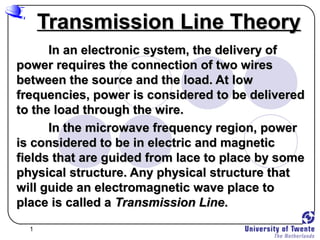
  • 1. 1 Transmission Line TheoryTransmission Line Theory In an electronic system, the delivery ofIn an electronic system, the delivery of power requires the connection of two wirespower requires the connection of two wires between the source and the load. At lowbetween the source and the load. At low frequencies, power is considered to be deliveredfrequencies, power is considered to be delivered to the load through the wire.to the load through the wire. In the microwave frequency region, powerIn the microwave frequency region, power is considered to be in electric and magneticis considered to be in electric and magnetic fields that are guided from lace to place by somefields that are guided from lace to place by some physical structure. Any physical structure thatphysical structure. Any physical structure that will guide an electromagnetic wave place towill guide an electromagnetic wave place to place is called aplace is called a Transmission LineTransmission Line..
  • 2. 2 Types of Transmission LinesTypes of Transmission Lines 1.1. Two wire lineTwo wire line 2.2. Coaxial cableCoaxial cable 3.3. WaveguideWaveguide  RectangularRectangular  CircularCircular 4.4. Planar Transmission LinesPlanar Transmission Lines  Strip lineStrip line  Microstrip lineMicrostrip line  Slot lineSlot line  Fin lineFin line  Coplanar WaveguideCoplanar Waveguide  Coplanar slot lineCoplanar slot line
  • 3. 3 Analysis of differences between Low and HighAnalysis of differences between Low and High FrequencyFrequency  At low frequencies, the circuit elements are lumpedAt low frequencies, the circuit elements are lumped since voltage and current waves affect the entire circuitsince voltage and current waves affect the entire circuit at the same time.at the same time.  At microwave frequencies, such treatment of circuitAt microwave frequencies, such treatment of circuit elements is not possible since voltag and current waveselements is not possible since voltag and current waves do not affect the entire circuit at the same time.do not affect the entire circuit at the same time.  The circuit must be broken down into unit sectionsThe circuit must be broken down into unit sections within which the circuit elements are considered to bewithin which the circuit elements are considered to be lumped.lumped.  This is because the dimensions of the circuit areThis is because the dimensions of the circuit are comparable to the wavelength of the waves accordingcomparable to the wavelength of the waves according to the formula:to the formula: c/fc/f where,where, c = velocity of lightc = velocity of light f = frequency of voltage/currentf = frequency of voltage/current
  • 5. 5 Metallic Cable Transmission MediaMetallic Cable Transmission Media • Metallic transmission linesMetallic transmission lines • Balanced and Unbalanced Transmission LinesBalanced and Unbalanced Transmission Lines • Metallic Transmission Line Equivalent CircuitMetallic Transmission Line Equivalent Circuit • Wave Propagation on a Metallic Transmission LineWave Propagation on a Metallic Transmission Line • Transmission Line LossesTransmission Line Losses • Phasor Current and VoltagesPhasor Current and Voltages • Single section of transmission lineSingle section of transmission line • Characteristic Impedance and PropagationCharacteristic Impedance and Propagation ConstantConstant • Standing waves, reflectionStanding waves, reflection
  • 6. 6 Types of Transmission LinesTypes of Transmission Lines CoaxialCoaxial Twisted-PairTwisted-Pair Open-WireOpen-Wire Twin-LeadTwin-Lead
  • 7. 7 Metallic transmission linesMetallic transmission lines Open-wireOpen-wire Twin leadTwin lead
  • 8. 8 Metallic transmission linesMetallic transmission lines Unshielded twisted-pairUnshielded twisted-pair
  • 9. 9 Metallic transmission linesMetallic transmission lines Coaxial cableCoaxial cable
  • 10. 10 Coaxial componentsCoaxial components  ConnectorsConnectors: Microwave coaxial connectors required to: Microwave coaxial connectors required to connect two coaxial lines are als calledconnect two coaxial lines are als called connector pairsconnector pairs (male(male andand female).female). They must match the characteristicThey must match the characteristic impedance of the attached lines and be designed to haveimpedance of the attached lines and be designed to have minimum reflection coefficients and not radiate powerminimum reflection coefficients and not radiate power through the connector.through the connector. E.g. APC-3.5, BNC, SMA, SMCE.g. APC-3.5, BNC, SMA, SMC  Coaxial sectionsCoaxial sections: Coaxial line sections slip inside each: Coaxial line sections slip inside each other while still making electrical contact. These sections areother while still making electrical contact. These sections are useful for matching loads and making slotted lineuseful for matching loads and making slotted line measurements. Double and triple stub tuning configurationsmeasurements. Double and triple stub tuning configurations are available as coaxial stub tuning sections.are available as coaxial stub tuning sections.  AttenuatorsAttenuators: The function of an attenuator is to reduce the: The function of an attenuator is to reduce the power of the signal through it by a fixed or adjustablepower of the signal through it by a fixed or adjustable amount. The different types of attenuators are:amount. The different types of attenuators are: 1.1. Fixed attenuatorsFixed attenuators 2.2. Step attenuatorsStep attenuators 3.3. Variable attenuatorsVariable attenuators
  • 11. 11 Coaxial components (contd.)Coaxial components (contd.)  Coaxial cavities: Coaxial cavities are concentricCoaxial cavities: Coaxial cavities are concentric lines or coaxial lines with an air dielectric andlines or coaxial lines with an air dielectric and closed ends. Propagation of EM waves is in TEMclosed ends. Propagation of EM waves is in TEM mode.mode.  Coaxial wave meters: Wave meters use a cavityCoaxial wave meters: Wave meters use a cavity to allow the transmission or absorption of ato allow the transmission or absorption of a wave at a frequency equal to the resonantwave at a frequency equal to the resonant frequency of the cavity. Coaxial cavities arefrequency of the cavity. Coaxial cavities are used as wave meters.used as wave meters.
  • 12. 12 AttenuatorsAttenuators Attenuators are components that reduce the amountAttenuators are components that reduce the amount of power a fixed amount, a variable amount or in aof power a fixed amount, a variable amount or in a series of fixed steps from the input to the output of theseries of fixed steps from the input to the output of the device. They operate on the principle of interfering withdevice. They operate on the principle of interfering with the electric field or magnetic field or both.the electric field or magnetic field or both.  Slide vane attenuatorsSlide vane attenuators: They work on the principle that a: They work on the principle that a resistive material placed in parallel with the E-lines of aresistive material placed in parallel with the E-lines of a field current will induce a current in the material that willfield current will induce a current in the material that will result inresult in II22 RR power loss.power loss.  Flap attenuatorFlap attenuator: A flap attenuator has a vane that is: A flap attenuator has a vane that is dropped into the waveguide through a slot in the top ofdropped into the waveguide through a slot in the top of the guide. The further the vane is inserted into thethe guide. The further the vane is inserted into the waveguide, the greater the attenuation.waveguide, the greater the attenuation.  Rotary vane attenuatorRotary vane attenuator: It is a precision waveguide: It is a precision waveguide attenuator in which attenuation follows a mathematicalattenuator in which attenuation follows a mathematical law. In this device, attenuation is independent onlaw. In this device, attenuation is independent on frequency.frequency.
  • 13. 13 IsolatorsIsolators Mismatch or discontinuities cause energy to beMismatch or discontinuities cause energy to be reflected back down the line. Reflected energy isreflected back down the line. Reflected energy is undesirable. Thus, to prevent reflected energy fromundesirable. Thus, to prevent reflected energy from reaching the source, isolators are used.reaching the source, isolators are used.  Faraday Rotational IsolatorFaraday Rotational Isolator: It combines ferrite: It combines ferrite material to shift the phase of an electromagneticmaterial to shift the phase of an electromagnetic wave in its vicinity and attenuation vanes towave in its vicinity and attenuation vanes to attenuate an electric field that is parallel to theattenuate an electric field that is parallel to the resistive plane.resistive plane.  Resonant absorption isolatorResonant absorption isolator: A device that can be: A device that can be used for higher powers. It consists of a section ofused for higher powers. It consists of a section of rectangular waveguide with ferrite material placedrectangular waveguide with ferrite material placed half way to the center of the waveguide, along thehalf way to the center of the waveguide, along the axis of the guide.axis of the guide.
  • 14. 14 Metallic transmission linesMetallic transmission lines Balanced lines have equal impedances from the twoBalanced lines have equal impedances from the two conductors to groundconductors to ground Twisted-pair and parallel lines are usually balancedTwisted-pair and parallel lines are usually balanced Differential, or balanced, transmission systemDifferential, or balanced, transmission system
  • 15. 15 Metallic transmission linesMetallic transmission lines Differential, or balanced, transmission systemDifferential, or balanced, transmission system signal voltagessignal voltages noise voltagesnoise voltages
  • 16. 16 Metallic transmission linesMetallic transmission lines Unbalanced lines usually have one conductor groundedUnbalanced lines usually have one conductor grounded Coaxial lines usually have outer conductor groundedCoaxial lines usually have outer conductor grounded Single-ended, or unbalanced, transmission systemSingle-ended, or unbalanced, transmission system
  • 17. 17 Ideal Transmission LineIdeal Transmission Line No lossesNo losses  conductors have zero resistanceconductors have zero resistance  dielectric has zero conductancedielectric has zero conductance  possible only with superconductorspossible only with superconductors  approximated by a short lineapproximated by a short line No capacitance or inductanceNo capacitance or inductance  possible with a real line only at dcpossible with a real line only at dc  with low frequencies and short lines thiswith low frequencies and short lines this can be approximatedcan be approximated
  • 18. 18 Two-wire parallel transmission lineTwo-wire parallel transmission line electrical equivalent circuitelectrical equivalent circuit
  • 19. 19 Traveling waveTraveling wave ( ) ( )coscv t V tω= ωω is the angular frequency (rad/sec)is the angular frequency (rad/sec) The input voltage can be described asThe input voltage can be described as
  • 20. 20 Traveling waveTraveling wave ( ) ( )coscv t V tω= ( ) ( ), coscv z t V t zω β= − ωω is the angular frequency (rad/sec)is the angular frequency (rad/sec) The input voltage can be described asThe input voltage can be described as ββ is the propagation constant (rad/m)is the propagation constant (rad/m) ( ) ( ), cosci z t I t zω β= − current and voltage are in phase?!?!?current and voltage are in phase?!?!? The traveling wave can be described asThe traveling wave can be described as
  • 21. 21 Phase velocity and wavelengthPhase velocity and wavelength ( ) ( )coscv t V t zω β= − 2βλ π= 2π β λ = distance 1time pv f f λ ω λ β = = = = 2 fω π= The energy travels with the group velocityThe energy travels with the group velocity g d v d ω β =
  • 22. 22 AttenuationAttenuation ( ) ( ), cosz cv z t V e t zα ω β− = − αα is the attenuation coefficientis the attenuation coefficient (nepers/meter)(nepers/meter) What is the attenuation in dB perWhat is the attenuation in dB per meter?meter?
  • 23. 23 AttenuationAttenuation ( ) ( ), cosz cv z t V e t zα ω β− = − αα is the attenuation coefficient (nepers/meter)is the attenuation coefficient (nepers/meter) What is the attenuation in dB per meter?What is the attenuation in dB per meter? ( ) ( )20log 20 log 8.686dB m Att e eα α α= = = (One neper is 8.686 dB)(One neper is 8.686 dB) ( ) ( )log logg a ax g x=
  • 24. 24 Phasor currents and voltagesPhasor currents and voltages A phasor can be used to represent the amplitude of aA phasor can be used to represent the amplitude of a sinusoidal voltage or current and is phase difference fromsinusoidal voltage or current and is phase difference from a reference sinusoid of the same frequency. A phasora reference sinusoid of the same frequency. A phasor does not include any representation of the frequency.does not include any representation of the frequency. ( ) ( ) ( )cos Rez z j z j t v t Ve t z Ve e eα α β ω ω β− − − = − = has a phasorhas a phasor VV which can be represented inwhich can be represented in amplitude-angle form asamplitude-angle form as VV∠φ∠φ,, or in componentor in component formform a+a+jjbb wherewhere a=Va=Vcoscosφφ andand b=Vb=Vsinsinφφ or in complex-or in complex- exponential formexponential form j Ve φ
  • 25. 25 The phasor of the driving voltage isThe phasor of the driving voltage is VV00 The phasor of the voltage at distanceThe phasor of the voltage at distance xx from the driving point isfrom the driving point is ( )jj xx x x e e e eα βα β γ− +− − − = = =x 0 0 0V V V V wherewhere γγ is the propagation constantis the propagation constant Phasor currents and voltagesPhasor currents and voltages jγ α β= +
  • 26. 26 z z e e γ γ − − = = x 0 x 0 V V I I Remember,Remember, II00 andand VV00 are themselves phasors,are themselves phasors, and their angles are not necessarily the same.and their angles are not necessarily the same. Phasor currents and voltagesPhasor currents and voltages jγ α β= +
  • 27. 27 Transmission Line ModelTransmission Line Model  At low frequencies only resistance has toAt low frequencies only resistance has to be consideredbe considered  At higher frequencies capacitance andAt higher frequencies capacitance and inductance must be includedinductance must be included  All of these are distributed along the lineAll of these are distributed along the line
  • 28. 28 Iz GδzCδz Iz Iz+δI Iz+δI Vz Vz+δV Total series resistanceTotal series resistance RRδδzz Total series inductanceTotal series inductance LLδδzz jR z L zδ δ ω δ= − −z zV I I ( )j d R L dz ω= − +z z V I ( )j d G C dz ω= − +z z I V ( )jR Lγ ω= − +z zV I ( )jG Cγ ω= − +z zI V Single section of transmission lineSingle section of transmission line C L 1 j j z z z z e e Z C Z L γ γ ω ω − − = = = = 0 0 V V I I δI jI G z C zδ δ ω δ= − −z zV V δV
  • 29. 29 Characteristic ImpedanceCharacteristic Impedance Ratio between voltage and current on lineRatio between voltage and current on line Depends only on line geometry andDepends only on line geometry and dielectricdielectric Not a function of lengthNot a function of length Has units of ohms but not the same as theHas units of ohms but not the same as the resistance of the wire in the lineresistance of the wire in the line 0Z = z z V I
  • 30. 30 ( )jR Lγ ω= − +z zV I ( )jG Cγ ω= − +z zI V 0 j j R L Z G C ω ω + = = + z z V I Characteristic ImpedanceCharacteristic Impedance j j R L G C ω ω + = + z z z z V I I V ZZ00 is the characteristic impedanceis the characteristic impedance For an RF lineFor an RF line RR andand GG are zero (valid for high RF frequencies)are zero (valid for high RF frequencies) 0 L Z C = =z z V I Current and voltage are in phaseCurrent and voltage are in phase RR = conductor resistance in= conductor resistance in ΩΩ/unit length/unit length LL = inductance in H/unit length= inductance in H/unit length GG = dielectric conductance in S/unit length= dielectric conductance in S/unit length CC = capacitance in F/unit length= capacitance in F/unit length
  • 31. 31 Velocity FactorVelocity Factor Step moves down line at a finite speedStep moves down line at a finite speed Velocity cannot be greater than speedVelocity cannot be greater than speed of light and is usually lowerof light and is usually lower Velocity factor is ratio between actualVelocity factor is ratio between actual propagation velocity and speed of lightpropagation velocity and speed of light Velocity factor depends only on lineVelocity factor depends only on line dielectricdielectric
  • 32. 32 Velocity FactorVelocity Factor  vvpp = propagation velocity on the line= propagation velocity on the line  cc = speed of light in vacuum= speed of light in vacuum == 300300 ×× 101066 m/sm/s c v v p f = 0 0 1 c µ ε =
  • 33. 33 Propagation ConstantPropagation Constant ( )jR Lγ ω= − +z zV I ( )jG Cγ ω= − +z zI V ( ) ( )2 j jR L G Cγ ω ω= + +z z z zV I V I ( ) ( )j jR L G Cγ ω ω= + + For anFor an ideal lineideal line RR andand GG are zeroare zero j LCγ ω= purely imaginary and no attenuationpurely imaginary and no attenuation jγ α β= + 0α = LCβ ω= 1 pv LC = pv ω β =
  • 34. 34 Metallic transmission linesMetallic transmission lines Two-wire parallel transmission lineTwo-wire parallel transmission line 0 276log D Z r = ZZ00 = the characteristic impedance (ohms)= the characteristic impedance (ohms) DD = the distance between the centers= the distance between the centers rr = the radius of the conductor= the radius of the conductor εε00 = the permittivity of free space (F/m)= the permittivity of free space (F/m) εεrr = the relative permittivity or dielectric constant of= the relative permittivity or dielectric constant of the medium (unitless)the medium (unitless) µµ00 = the permeability of free space (H/m)= the permeability of free space (H/m) 1 p o v µ ε = 0rε ε ε= 0 1 o c µ ε =
  • 35. 35 Metallic transmission linesMetallic transmission lines Coaxial cableCoaxial cable 0 138 log r D Z dε = ZZ00 = the characteristic impedance (ohms)= the characteristic impedance (ohms) DD = the diameter of the outer conductor= the diameter of the outer conductor dd = the diameter of the inner conductor= the diameter of the inner conductor ε = the permittivity of the material= the permittivity of the material εεrr = the relative permittivity or dielectric constant= the relative permittivity or dielectric constant of the mediumof the medium µµ00 = the permeability of free space= the permeability of free space 1 p o v µ ε = 0rε ε ε= 0 1 o c µ ε =
  • 36. 36 Transmission Lines LossesTransmission Lines Losses • Conductor LossesConductor Losses •Increases with frequencyIncreases with frequency due to skin effectdue to skin effect • Dielectric Heating LossesDielectric Heating Losses •Also increases withAlso increases with frequencyfrequency • Radiation LossesRadiation Losses • Not significant with goodNot significant with good quality coax properlyquality coax properly installedinstalled • Can be a problem withCan be a problem with open-wire cableopen-wire cable • Coupling LossesCoupling Losses • CoronaCorona Skin effect
  • 38. 38
  • 39. 39 Step Applied to Infinite LineStep Applied to Infinite Line Voltage step will propagate down lineVoltage step will propagate down line Energy is stored in line capacitance andEnergy is stored in line capacitance and inductanceinductance Energy from source appears to be dissipatedEnergy from source appears to be dissipated by line but is really storedby line but is really stored If line is infinitely long the step never reachesIf line is infinitely long the step never reaches the endthe end Voltage and current have definite, finite valuesVoltage and current have definite, finite values
  • 40. 40 Reflection of Voltage StepReflection of Voltage Step Infinite line: no reflectionInfinite line: no reflection Finite line with load impedanceFinite line with load impedance ZZLL == ZZ00  no reflectionno reflection  the load looks to the source like an extension ofthe load looks to the source like an extension of the linethe line  Voltage and currents are compatibleVoltage and currents are compatible  Z =Z = √√(L/C)(L/C) Finite line with load impedanceFinite line with load impedance ZZLL ≠≠ ZZ00  Some or all of the step will reflect from the loadSome or all of the step will reflect from the load end of the lineend of the line
  • 41. 41 Reflection of PulsesReflection of Pulses Transmission LineTransmission Line Short circuitShort circuit R0 ReflectionReflection hyperlinkhyperlink
  • 42. 42 Shorted LineShorted Line  Total voltage at shorted end = 0Total voltage at shorted end = 0  Incident and reflected voltages must beIncident and reflected voltages must be equal and oppositeequal and opposite  Incident and reflected currents are equalIncident and reflected currents are equal with same polaritywith same polarity  Time for surge to reach end of line isTime for surge to reach end of line is T = L/vT = L/vpp
  • 43. 43 Open LineOpen Line Transmission LineTransmission Line R0 Reflection of PulsesReflection of Pulses ReflectionReflection hyperlinkhyperlink
  • 44. 44 Open-Circuited LineOpen-Circuited Line Total current at open end = 0Total current at open end = 0 Incident and reflected currents must beIncident and reflected currents must be equal and oppositeequal and opposite Incident and reflected voltages are equalIncident and reflected voltages are equal with same polaritywith same polarity Time for surge to reach end of line isTime for surge to reach end of line is T = L/vT = L/vpp
  • 45. 45 Reflection CoefficientReflection Coefficient More complex situation: Load has an arbitraryMore complex situation: Load has an arbitrary impedanceimpedance  not equal tonot equal to ZZ00  not shorted or opennot shorted or open  impedance may be complex (either capacitive orimpedance may be complex (either capacitive or inductive as well as resistive)inductive as well as resistive) When the ZL ≠ Z0, part of the power is reflected back and the remainder is absorbed by the load.
  • 46. 46 Reflection CoefficientReflection Coefficient r r i i V I or V I Γ = ΓΓ = reflection coefficient= reflection coefficient VVii = incident voltage= incident voltage VVrr = reflected voltage= reflected voltage IIii = incident current= incident current IIrr = reflected current= reflected current The amount of voltage reflected back isThe amount of voltage reflected back is calledcalled voltage reflection coefficient.voltage reflection coefficient.
  • 47. 47 ZZLL Transmission LineTransmission Line ZZ00 Reflection of PulsesReflection of Pulses r r i i V I or V I Γ @ total voltage i rV V= + total current i rI I= − i r L i r V V Z I I + = − 0 i r i r V V Z I I = = 0 0 L L Z Z Z Z − Γ = +
  • 48. 48 Wave Propagation on LinesWave Propagation on Lines  Start by assuming a matched lineStart by assuming a matched line  Waves move down the line at propagationWaves move down the line at propagation velocityvelocity  Waves are the same at all points exceptWaves are the same at all points except for phasefor phase  Phase changes 360 degrees in thePhase changes 360 degrees in the distance a wave travels in one perioddistance a wave travels in one period  This distance is called the wavelengthThis distance is called the wavelength
  • 49. 49 Standing WavesStanding Waves  When an incident wave reflects from a mismatchedWhen an incident wave reflects from a mismatched load, an interference pattern developsload, an interference pattern develops  Both incident and reflected waves move at theBoth incident and reflected waves move at the propagation velocity, but the interference pattern ispropagation velocity, but the interference pattern is stationarystationary  The interference pattern is called a set of standingThe interference pattern is called a set of standing waveswaves  It is formed by the addition of incident and reflectedIt is formed by the addition of incident and reflected waves and has nodal points that remain stationarywaves and has nodal points that remain stationary with timewith time
  • 50. 50 Incident and Reflected WavesIncident and Reflected Waves
  • 52. 52 Standing-Wave RatioStanding-Wave Ratio When line is mismatched but neitherWhen line is mismatched but neither open nor shorted, voltage varies alongopen nor shorted, voltage varies along line without ever falling to zeroline without ever falling to zero Greater mismatch leads to greaterGreater mismatch leads to greater variationvariation Voltage standing-wave ratio (VSWR orVoltage standing-wave ratio (VSWR or SWR) is defined:SWR) is defined: min max V V SWR = (( ≥≥ 1)1)
  • 53. 53 Standing wavesStanding waves max min V SWR V = max i r i iV V V V V= + = + Γ min i r i iV V V V V= − = − Γ 0 0 1 or 1 L L Z Z SWR Z Z + Γ = = − Γ 1 1 SWR SWR − Γ = + 0 0 L L Z Z Z Z − Γ = + ( ≥ 1)
  • 54. 54 SWR and Reflection CoefficientSWR and Reflection Coefficient SWR is a positive real numberSWR is a positive real number ΓΓ may be positive, negative or complexmay be positive, negative or complex SWRSWR ≥≥ 11 Magnitude ofMagnitude of ΓΓ ≤≤ 11
  • 55. 55 Standing waves on an Open LineStanding waves on an Open Line This is only the amplitude!!!This is only the amplitude!!!
  • 56. 56 Standing waves on an Shorted LineStanding waves on an Shorted Line This is only the amplitude!!!This is only the amplitude!!!
  • 57. 57 Effects of High SWREffects of High SWR High SWR causes voltage peaks onHigh SWR causes voltage peaks on the line that can damage the line orthe line that can damage the line or connected equipment such as aconnected equipment such as a transmittertransmitter Current peaks due to high SWR causeCurrent peaks due to high SWR cause losses to increaselosses to increase
  • 58. 58 Reflected PowerReflected Power When a signal travels down a mismatched line,When a signal travels down a mismatched line, some of the power reflects from the loadsome of the power reflects from the load This power is dissipated in the source, if theThis power is dissipated in the source, if the source matches the linesource matches the line A high SWR causes the load power to be reducedA high SWR causes the load power to be reduced
  • 59. 59 Reflected PowerReflected Power PPrr = reflected power= reflected power PPii = incident power= incident power PPLL = power delivered to load= power delivered to load 1 1 SWR SWR − Γ = + iL iL ir P SWR SWR P PP PP 2 2 2 )1( 4 )1( + = Γ−= Γ=
  • 60. 60 Time-Domain ReflectometryTime-Domain Reflectometry 2 v t d × = ReflectoReflecto metermeter transmission linetransmission line reflectionreflection
  • 61. 61 General Input Impedance EquationGeneral Input Impedance Equation Input impedance of a transmission lineInput impedance of a transmission line at a distanceat a distance LL from the loadfrom the load impedance Zimpedance ZLL with a characteristic Zwith a characteristic Zoo isis Zinput =Zinput = ZZoo [(Z[(ZLL + j Z+ j Zoo BL)BL) (Z(Zoo + j Z+ j ZLL BL)]BL)] where B is called phase constant orwhere B is called phase constant or wavelength constant and is defined bywavelength constant and is defined by the equationthe equation B = 2B = 2
  • 62. 62 Half and Quarter wave transmission lines  The relationship of the input impedance at the input of the half-wave transmission line with its terminating impedance is got by letting L = in the impedance equation. Zinput = ZL   The relationship of the input impedance at the input of the quarter-wave transmission line with its terminating impedance is got by letting L = in the impedance equation. Zinput = √(Zinput Zoutput) 
  • 63. 63 Effect of Lossy line on V and I wavesEffect of Lossy line on V and I waves  The effect of resistance in a transmission line is toThe effect of resistance in a transmission line is to continuously reduce the amplitude of both incidentcontinuously reduce the amplitude of both incident and reflected voltage and current waves.and reflected voltage and current waves.  Skin Effect: As frequency increases, depth ofSkin Effect: As frequency increases, depth of penetration into adjacent conductive surfacespenetration into adjacent conductive surfaces decreases for boundary currents associated withdecreases for boundary currents associated with electromagnetic waves, that results in theelectromagnetic waves, that results in the confinement of the voltage and current waves at theconfinement of the voltage and current waves at the boundary of the transmission line, thus making theboundary of the transmission line, thus making the transmission more lossy.transmission more lossy. Skin depth (m) = 1Skin depth (m) = 1 √√ff where f = frequency, Hzwhere f = frequency, Hz = permeability, H/m= permeability, H/m = conductivity, S/m= conductivity, S/m
  • 64. 64 Smith chart  For complex transmission line problems, the use of the formulae becomes increasingly difficult and inconvenient. An indispensable graphical method of solution is the use of Smith Chart.
  • 65. 65 Components of a Smith ChartComponents of a Smith Chart  HHorizontal lineorizontal line: The horizontal line running through: The horizontal line running through the center of the Smith chart represents either thethe center of the Smith chart represents either the resistive or the conductive component. Zeroresistive or the conductive component. Zero resistance is located on the left end and infiniteresistance is located on the left end and infinite resistance is located on the right end of the line.resistance is located on the right end of the line.  CCircles of constant resistance and conductanceircles of constant resistance and conductance:: Circles of constant resistance are drawn on the SmithCircles of constant resistance are drawn on the Smith chart tangent to the right-hand side of the chart andchart tangent to the right-hand side of the chart and its intersection with the centerline. These circles ofits intersection with the centerline. These circles of constant resistance are used to locate complexconstant resistance are used to locate complex impedances.impedances.  LLines of constant reactanceines of constant reactance: Lines of constant: Lines of constant reactance are shown on the Smith chart with curvesreactance are shown on the Smith chart with curves that start from a given reactance value on the outerthat start from a given reactance value on the outer circle and end at the right-hand side of the center line.circle and end at the right-hand side of the center line.
  • 66. 66 Type of Microwave problems that SmithType of Microwave problems that Smith chart can be usedchart can be used 1.1. Plotting a complex impedance on a Smith chartPlotting a complex impedance on a Smith chart 2.2. Finding VSWR for a given loadFinding VSWR for a given load 3.3. Finding the admittance for a given impedanceFinding the admittance for a given impedance 4.4. Finding the input impedance of a transmission lineFinding the input impedance of a transmission line terminated in a short or open.terminated in a short or open. 5.5. Finding the input impedance at any distance from aFinding the input impedance at any distance from a load Zload ZLL.. 6.6. Locating the first maximum and minimum from anyLocating the first maximum and minimum from any loadload 7.7. Matching a transmission line to a load with a singleMatching a transmission line to a load with a single series stub.series stub. 8.8. Matching a transmission line with a single parallel stubMatching a transmission line with a single parallel stub 9.9. Matching a transmission line to a load with twoMatching a transmission line to a load with two parallel stubs.parallel stubs.
  • 67. 67 Plotting a Complex Impedance on aPlotting a Complex Impedance on a Smith ChartSmith Chart  To locate a complex impedance, Z = R+-jX orTo locate a complex impedance, Z = R+-jX or admittance Y = G +- jB on a Smith chart,admittance Y = G +- jB on a Smith chart, normalize the real and imaginary part of thenormalize the real and imaginary part of the complex impedance. Locating the value of thecomplex impedance. Locating the value of the normalized real term on the horizontal linenormalized real term on the horizontal line scale locates the resistance circle. Locatingscale locates the resistance circle. Locating the normalized value of the imaginary term onthe normalized value of the imaginary term on the outer circle locates the curve of constantthe outer circle locates the curve of constant reactance. The intersection of the circle andreactance. The intersection of the circle and the curve locates the complex impedance onthe curve locates the complex impedance on the Smith chart.the Smith chart.
  • 68. 68 Finding the VSWR for a givenFinding the VSWR for a given loadload  Normalize the load and plot its location onNormalize the load and plot its location on the Smith chart.the Smith chart.  Draw a circle with a radius equal to theDraw a circle with a radius equal to the distance between the 1.0 point and thedistance between the 1.0 point and the location of the normalized load and thelocation of the normalized load and the center of the Smith chart as the center.center of the Smith chart as the center.  The intersection of the right-hand side ofThe intersection of the right-hand side of the circle with the horizontal resistancethe circle with the horizontal resistance line locates the value of the VSWR.line locates the value of the VSWR.
  • 69. 69 Finding the Input Impedance at anyFinding the Input Impedance at any Distance from the LoadDistance from the Load  The load impedance is first normalized and isThe load impedance is first normalized and is located on the Smith chart.located on the Smith chart.  The VSWR circle is drawn for the load.The VSWR circle is drawn for the load.  A line is drawn from the 1.0 point through theA line is drawn from the 1.0 point through the load to the outer wavelength scale.load to the outer wavelength scale.  To locate the input impedance on a SmithTo locate the input impedance on a Smith chart of the transmission line at any givenchart of the transmission line at any given distance from the load, advance in clockwisedistance from the load, advance in clockwise direction from the located point, a distance indirection from the located point, a distance in wavelength equal to the distance to the newwavelength equal to the distance to the new location on the transmission line.location on the transmission line.
  • 70. 70 Power LossPower Loss  Return Power LossReturn Power Loss: When an electromagnetic: When an electromagnetic wave travels down a transmission line andwave travels down a transmission line and encounters a mismatched load or aencounters a mismatched load or a discontinuity in the line, part of the incidentdiscontinuity in the line, part of the incident power is reflected back down the line. Thepower is reflected back down the line. The return loss is defined as:return loss is defined as: PPreturnreturn = 10 log= 10 log1010 PPii/P/Prr PPreturnreturn = 20 log= 20 log1010 1/1/  Mismatch Power LossMismatch Power Loss: The term mismatch loss: The term mismatch loss is used to describe the loss caused by theis used to describe the loss caused by the reflection due to a mismatched line. It is definedreflection due to a mismatched line. It is defined asas PPmismatchmismatch = 10 log= 10 log1010 PPii/(P/(Pii - P- Prr))
  • 71. 71 Notes:Notes:  Metallic circuit currentMetallic circuit current – currents that flow in– currents that flow in opposite directions in a balanced wire pairopposite directions in a balanced wire pair  Longitudinal currentLongitudinal current – currents that flow in the– currents that flow in the same directionsame direction  Common Mode Rejection (CMR)Common Mode Rejection (CMR) – cancellation– cancellation of common mode signals or noise interferenceof common mode signals or noise interference induced equally on both wires producinginduced equally on both wires producing longitudinal currents that cancel in the loadlongitudinal currents that cancel in the load CMRR = 40 to 70 dBCMRR = 40 to 70 dB
  • 72. 72 Notes:Notes:  Primary electrical constantsPrimary electrical constants – R, L, C, G– R, L, C, G  Secondary constantsSecondary constants – Zo, Propagation– Zo, Propagation ConstantConstant  For maximum power transfer, ZFor maximum power transfer, ZLL = Zo, thus no= Zo, thus no reflectionreflection  Characteristic impedance = Surge impedanceCharacteristic impedance = Surge impedance  Transmission line stores energy in itsTransmission line stores energy in its distributed inductance and capacitancedistributed inductance and capacitance
  • 73. 73 Notes:Notes:  Transmission lines:Transmission lines:  The input impedance of an infinitely long line at radioThe input impedance of an infinitely long line at radio frequencies is resistive and equal to Zofrequencies is resistive and equal to Zo  Nonresonant – when electromagnetic waves travelNonresonant – when electromagnetic waves travel the line without reflectionsthe line without reflections  Ratio of voltage to current at any point is equal to ZoRatio of voltage to current at any point is equal to Zo  Incident voltage and current at any point are in phaseIncident voltage and current at any point are in phase  Line losses on a non-resonant line are minimum perLine losses on a non-resonant line are minimum per unit lengthunit length  Any transmission line that is terminated in a loadAny transmission line that is terminated in a load equals to Zo acts as if it were an infinite line.equals to Zo acts as if it were an infinite line.  Prop. Cons. = attenuation coeff. + phase shift coeff.Prop. Cons. = attenuation coeff. + phase shift coeff. γγ == αα + j+ jββ
  • 74. 74 Notes:Notes: MaterialMaterial Velocity FactorVelocity Factor airair 0.95 – 0.9750.95 – 0.975 rubberrubber 0.56 – 0.650.56 – 0.65 polyethylenepolyethylene 0.660.66 teflonteflon 0.700.70 teflon foamteflon foam 0.820.82 teflon pinsteflon pins 0.810.81 teflon spiralteflon spiral 0.810.81
  • 75. 75 Notes:Notes: MaterialMaterial Dielectric ConstantDielectric Constant VacuumVacuum 11 AirAir 1.00061.0006 TeflonTeflon 2.12.1 polyethylenepolyethylene 2.272.27 polystyrenepolystyrene 2.52.5 paper, paraffinedpaper, paraffined 2.52.5 rubberrubber 3.03.0 PVCPVC 3.33.3 MicaMica 5.05.0 GlassGlass 7.57.5
  • 76. 76 Notes:Notes:  Velocity factor (Velocity constant) =Velocity factor (Velocity constant) = actual vel. Of prop.actual vel. Of prop. vel. In free spacevel. In free space Vf = Vp / cVf = Vp / c  Electrical length of transmission lineElectrical length of transmission line  Long – length exceedsLong – length exceeds λλ/16/16  Short – length less than or equalShort – length less than or equal λλ/16/16  Delay lines – transmission lines designed toDelay lines – transmission lines designed to intentionally introduce a time delay in the path of anintentionally introduce a time delay in the path of an electromagnetic waveelectromagnetic wave td = LC (seconds)td = LC (seconds) td = 1.016td = 1.016 ЄЄ
  • 77. 77 Notes:Notes:  The disadvantages of not having a matched line:The disadvantages of not having a matched line:  100 percent of the source incident power does not100 percent of the source incident power does not reach the loadreach the load  The dielectric separating the two conductors canThe dielectric separating the two conductors can break down and cause corona due to high VSWRbreak down and cause corona due to high VSWR  Reflections and rereflections cause more power lossReflections and rereflections cause more power loss  Reflections cause ghost imagesReflections cause ghost images  Mismatches cause noise interferenceMismatches cause noise interference
  • 78. 78 Notes:Notes:  Characteristics of transmission line terminated at openCharacteristics of transmission line terminated at open  voltage incident wave is reflected back (no phasevoltage incident wave is reflected back (no phase reversal)reversal)  current incident wave is reflected back 180 degreescurrent incident wave is reflected back 180 degrees from how it would have continuedfrom how it would have continued  sum of the incident and reflected current waveformssum of the incident and reflected current waveforms is minimumis minimum  sum of the incident and reflected voltage waveformssum of the incident and reflected voltage waveforms is maximumis maximum
  • 79. 79 Notes:Notes:  Characteristics of transmission line terminated at shortCharacteristics of transmission line terminated at short  voltage standing wave is reflected back 180 degreesvoltage standing wave is reflected back 180 degrees reversed from how it would have continuedreversed from how it would have continued  current standing wave is reflected back the same ascurrent standing wave is reflected back the same as if it had continuedif it had continued  sum of the incident and reflected current waveformssum of the incident and reflected current waveforms is maximumis maximum  sum of the incident and reflected voltage waveformssum of the incident and reflected voltage waveforms is zero at the shortis zero at the short
  • 80. 80 InputInput endend OutputOutput endend λλ/4/4 Zin = resistive, maxZin = resistive, max Zin = resistive, minZin = resistive, min Zin = inductiveZin = inductive Zin = capacitiveZin = capacitive Zin = capacitiveZin = capacitive Zin = inductiveZin = inductive shortshort openopen shortshort openopen shortshort openopen Input ImpedanceInput Impedance Parallel LC circuit,Parallel LC circuit, resistive and maximumresistive and maximum Series LC circuit,Series LC circuit, resistive and minimumresistive and minimum inductorinductor capacitorcapacitor capacitorcapacitor inductorinductor
  • 81. 81 Notes:Notes:  The impedance transformation for a quarter wavelengthThe impedance transformation for a quarter wavelength transmission line is:transmission line is:  RRLL = Zo: quarter= Zo: quarter λλ line acts 1:1 turns ratio transformerline acts 1:1 turns ratio transformer  RRLL > Zo: quarter> Zo: quarter λλ lineline acts as a step down transformeracts as a step down transformer  RRLL < Zo: quarter< Zo: quarter λλ line acts as a step up transformerline acts as a step up transformer  Characteristic Impedance of quarter wavelength X’formerCharacteristic Impedance of quarter wavelength X’former Zo’ =Zo’ = √(Zo√(ZoZZLL))  When a load is purely inductive oir purely capacitive, noWhen a load is purely inductive oir purely capacitive, no energy is absorbed, thus,energy is absorbed, thus, ГГ = 1 and SWR = inf.= 1 and SWR = inf.
  • 82. 82 Notes:Notes:  Stub MatchingStub Matching  Stubs are used to eliminate the reactive componentStubs are used to eliminate the reactive component to match the transmission line to the loadto match the transmission line to the load  It is just a piece of additional transmission line that isIt is just a piece of additional transmission line that is placed across the primary line as close to the load asplaced across the primary line as close to the load as possiblepossible  Susceptance of stub is used to tune out theSusceptance of stub is used to tune out the susceptance of the loadsusceptance of the load  Shorted stubs are preferred because open stubsShorted stubs are preferred because open stubs have the tendency to radiate at higher frequencieshave the tendency to radiate at higher frequencies
  • 83. 83 Notes:Notes:  Process of Stub MatchingProcess of Stub Matching  locate a point as close to the load as possible wherelocate a point as close to the load as possible where the conductive component of the input admittance isthe conductive component of the input admittance is equal to the characteristic admittance of transmissionequal to the characteristic admittance of transmission line Yin = G – jB, G = 1 / Zoline Yin = G – jB, G = 1 / Zo  Attach the shorted stub to the point on theAttach the shorted stub to the point on the transmission linetransmission line  Depending whether the reactive component at theDepending whether the reactive component at the point is inductive or capacitive, the stub length ispoint is inductive or capacitive, the stub length is adjustedadjusted Yin = Go – jB + jBstubYin = Go – jB + jBstub Yin = GoYin = Go
  • 84. 84 Notes:Notes:  Time Domain Reflectometry (TDR)Time Domain Reflectometry (TDR)  technique used to locate an impairment in thetechnique used to locate an impairment in the metallic cablemetallic cable  How much of the transmitted signal returns dependsHow much of the transmitted signal returns depends on the type and magnitude of the impairmenton the type and magnitude of the impairment  Impairment represents a discontinuity in the signalImpairment represents a discontinuity in the signal  For higher frequency applications (300 MHz – 3000 MHz),For higher frequency applications (300 MHz – 3000 MHz), microstrip and stripline is constructed to interconnectmicrostrip and stripline is constructed to interconnect components on PC boardscomponents on PC boards  When the distance between source and load ends is aWhen the distance between source and load ends is a few inches or less, coaxial cable is impracticalfew inches or less, coaxial cable is impractical  Microstrip and Stripline use the tracks on the PC board.Microstrip and Stripline use the tracks on the PC board.
  • 85. 85 Notes:Notes:  Microstrip and Stripline are used to constructMicrostrip and Stripline are used to construct transmission lines, inductors, capacitors, tuned circuits,transmission lines, inductors, capacitors, tuned circuits, filters, phase shifters, and impedance matching devices.filters, phase shifters, and impedance matching devices.  Microstrip – when the lines are etched in the middleMicrostrip – when the lines are etched in the middle layer of the multilayer PC boardlayer of the multilayer PC board Zo =Zo = 8787 lnln 5.98h__5.98h__ ЄЄ fiberglass = 4.5fiberglass = 4.5 √√((ЄЄ + 1.41)+ 1.41) 0.8w + t0.8w + t ЄЄ teflon = 3teflon = 3 w = width of Cu tracew = width of Cu trace t = thickness of Cu tracet = thickness of Cu trace h = thickness of dielectrich = thickness of dielectric  Stripline – if the lines are etched onto the surface of theStripline – if the lines are etched onto the surface of the PC board onlyPC board only Zo =Zo = 6060 lnln 4d __4d __ d = dielectric thickd = dielectric thick
  • 86. 86
  • 87. 87
  • 88. 88 Problems:Problems: 1.1. Determine the characteristic impedance for anDetermine the characteristic impedance for an air dielectric two-wire parallel transmissionair dielectric two-wire parallel transmission line with a D/r ratio = 13.5line with a D/r ratio = 13.5 (311.97 ohms)(311.97 ohms) 2.2. Determine the characteristic impedance for anDetermine the characteristic impedance for an RG-59A coaxial cable with parameters:RG-59A coaxial cable with parameters: L=0.121L=0.121 μμH/ft, C=30 pF/ft, d=0.042 in., D=0.22H/ft, C=30 pF/ft, d=0.042 in., D=0.22 in, andin, and ЄЄ=2.15=2.15 (63.509 ohms, 67.685 ohms)(63.509 ohms, 67.685 ohms) 3.3. For a given length of RG8A/U coaxial cableFor a given length of RG8A/U coaxial cable with parameters: C=98.4 pF/m, L=262.45 nH/m,with parameters: C=98.4 pF/m, L=262.45 nH/m, ЄЄr=2.15. Find Vp and Vfr=2.15. Find Vp and Vf (1.968x10(1.968x1088 m/s, 0.656m/s, 0.656 or 0.682)or 0.682)
  • 89. 89 Problems:Problems: 4.4. For a transmission line with incident voltage ofFor a transmission line with incident voltage of 5.2V and reflected voltage of 3.8V, find5.2V and reflected voltage of 3.8V, find reflection coefficient and SWRreflection coefficient and SWR (0.731, 6.429)(0.731, 6.429) 5.5. Determine the physical length and Zo for aDetermine the physical length and Zo for a quarter wavelength transformer that is used toquarter wavelength transformer that is used to match a section of RG8A/U (Zo=50 ohms) to amatch a section of RG8A/U (Zo=50 ohms) to a 175 ohm resistive load. The frequency of175 ohm resistive load. The frequency of operation is 220 MHz and the velocity factor isoperation is 220 MHz and the velocity factor is 11 (0.341 m, 93.54 ohms)(0.341 m, 93.54 ohms)
  • 90. 90 Stub MatchingStub Matching  Use to remove the reactive component of theUse to remove the reactive component of the complex impedance of the load to match thecomplex impedance of the load to match the transmission line to the loadtransmission line to the load  It is a piece of additional transmission line that isIt is a piece of additional transmission line that is placed across the primary line as close to the loadplaced across the primary line as close to the load as possibleas possible  The susceptance of the stub is used to tune out theThe susceptance of the stub is used to tune out the susceptance of the loadsusceptance of the load  Either a shorted or open stub is used with greaterEither a shorted or open stub is used with greater preference on the shorted stubpreference on the shorted stub  A transmission line that is one-half wavelength orA transmission line that is one-half wavelength or shorter is used to tune out the reactive componentshorter is used to tune out the reactive component of the loadof the load
  • 91. 91 Stub Matching ProcessStub Matching Process 1.1. Locate a point as close as possible to the loadLocate a point as close as possible to the load where the conductive component of the Zwhere the conductive component of the Zinin = Z= Zoo YYinin = G – jB where G = 1 / Z= G – jB where G = 1 / Zoo 2.2. Attach the shorted stub on the identified pointAttach the shorted stub on the identified point 3.3. Depending on whether the reactive component atDepending on whether the reactive component at that point is inductive or capacitive, the stub lengththat point is inductive or capacitive, the stub length is adjusted accordinglyis adjusted accordingly YYinin = G= Goo – jB + jB– jB + jBstubstub ~ Y~ Yinin = G= Goo