Introduction to FPGA and projects overview
•
0 likes•59 views

This presentation covers the basic overview of the FPGA impact in the consumer's electronics and some projects overview that was accomplished by using FPGA as a controller

Recommended
More Related Content
What's hot
What's hot (20)
Similar to Introduction to FPGA and projects overview
Similar to Introduction to FPGA and projects overview (20)
Recently uploaded
Recently uploaded (20)
Introduction to FPGA and projects overview
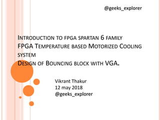
- 1. INTRODUCTION TO FPGA SPARTAN 6 FAMILY FPGA TEMPERATURE BASED MOTORIZED COOLING SYSTEM DESIGN OF BOUNCING BLOCK WITH VGA. @geeks_explorer Vikrant Thakur 12 may 2018 @geeks_explorer
- 2. 1.Programmable Logic 2.Evolution: TTL PLA CPLD FPGA ASIC 3.Development and research aspects 4.Using FPGA for high speed data processing 5.Reprograme ability which distinguishes FPGAs from Application Specific Integrated Circuits
- 3. Programmable Logic is Found Everywhere!
- 4. WHY FPGA? • In early years the digital circuits were designed manually using the techniques such as Boolean expressions , circuit schematics , Karnaugh maps etc. Most of the people used schematic based soft wares like p spice , h spice etc. • With the increasing device densities the choice of this traditional methods has become limited. • let us consider a design ,a 16 x 16 multiplier with schematic capture and using the HDL. • The multiplier is a complex arrangement of adders and registers . In the present case we have two 16 –bit inputs and one 32-bit product output .So , a total of 64 I/O s. Approximately the circuit requires 6000 equivalent gates. • Designing circuit by arranging 6000 gates requires lot of time and energy. In order to compensate that time and energy along with faster processing speed a company came up with solution called FPGA which can be programed with language VHDL (hardware description language).
- 5. Xilinx Spartan 6 FPGA board Project Board Board configuration: 16 Nos. Point LEDs (Logic Output) 2 Nos. of Push Buttons Two UART(RS232) 12-Bit SPI ADC (2 channel) 12-Bit SPI DAC Temperature Sensor LM35 5V SPDT Relay Buzzer (Alarm) Reset Button | Power-on Indication JTAG (Program/Debug) 40 Pin and 20 Pin I/O Expansion Connector On-Board Voltage regulators +5V | +3V3 | +1V2 FPGA Module Device : Spartan6 (XC6SLX9-TQ144) Memory : 4MB - PROM Clock : 50MHz crystal
- 6. PROJECT OVERVIEW • In two weeks ,learning how to program FPGA and program different Led blinking patterns and clock division method. • In third week we starting working on a project :FPGA based motorized cooling systems TEMPERATURE SENSOR MADE WITH THERMSISTOR ADC FPGA (Generating PWM which controlled the speed of motor.) H BRIDGE MOSFET (Design Controlling overall movement of Motor.)
- 7. ADC (analog to digital converter) The ADC input is analog signal such a current or voltage form and output as binary form (0 or 1). MCP 3202 microchip ADC commutes through SPI interface.
- 8. Timing Diagram of ADC
- 9. • PWM BLOCK DIAGRAM :- Pulse Width Modulation :- Pulse width modulation (PWM), or pulse-duration modulation (PDM), is modulation technique used to encode a message into a pulsing signal. Although his modulation technique can be used to encode information for transmission, its main use is to allow the control of the power supplied to electrical devices, especially to inertia loads such as motors.
- 10. Different PWM signal observed with change in the value received from ADC which indeed controlled the speed of DC motor.
- 11. H bridge transistor based circuit
- 12. Bouncing Ball with VGA interfaced with FPGA FPGA Controlling the movements onto screen along with graphics VGA (video graphics array) LED screen ALL are communicating with 25 MHZ clock speed and internal graphics on screen is controlled by 5MHZ.