SlideShare une entreprise Scribd logo
1  sur  92
Experiment 1
OBJECTIVE:
     Setting up Fiber Optic Analog Link Study of a 650nm fiber optic analog link in this experiment you will study the
relationship between the input signal and received signal.
Equipments Required:
        1. ST2502 trainer with power supply cord
        2. Optical Fiber cable
        3. Cathode ray oscilloscope with necessary connecting probe
Connection Diagram:
Procedure:
 1. Connect the power supply cord to the main power plug & to trainer ST2502.
 2. Ensure that all switched faults are ‘Off’.
 3. Make the following connections as shown in figure 1.1
       a. Connect the 1 KHz sine wave output to emitter l's input.
       b. Connect the Fiber Optics cable between emitter output and detectors input.
       c. Detector l's output to AC amplifier 1 input.
 4. On the board, switch emitter l's driver to analog mode.
 5. Switch ON the power supply of trainer and oscilloscope.
 6. Observe the input to emitter 1 (TP5) with the output from AC amplifier 1 (TP28) and note that
 the two signals are same.
Questions:
                 1. What is meant by index profile?
                 2. What is the drawback of multimode fibers?
                 3. What is fiber optics?
Experiment 2
OBJECTIVE:
Setting up Fiber Optic Digital Link Study of a 650 nm fiber optic digital link In this experiment you will study
the relationship between the input signal and received signal.
Equipments Required
        1. ST2502 trainer with power supply cord
        2. Optical Fiber cable
        3. Cathode ray oscilloscope with necessary connecting probe
Connection Diagram:
Procedure
1. Connect the power supply cord to the main the Power Supply to the board.
2. Ensure that all switched faults are ‘Off’.
3. Make the following connections as shown in figure 2.1.
            Connect the 1 KHz square wave output to emitter l's input.
            Connect the fiber optic cable between emitter output and detectors input.
            Detector 1's output to comparator 1’s input.
            Comparator l's output to AC amplifier l's input


4. On the board, switch emitter 1's driver to digital mode.
5. Switch ON the power supply of trainer and oscilloscope.
6. Monitor both the inputs to comparator 1 (TP13 & 14). Slowly adjust the Comparators bias preset,
until DC Level on the input (TP13) lays mid way between the high and low level of the signal on the
positive input (TP14).
7. Observe the input to emitter 1 (TP 5) with the output from AC amplifier 1 (TP28) and note that the
two signals are same.


Questions:
   1. Why single mode fibers are used for long distance transmission?
   2. What is optical fiber?
   3. What is step index profile?
Experiment 3
Objective:
Study of Intensity Modulation Technique using Analog input signal. To obtain intensity modulation of
the analog signal, transmit it over a fiber optic cable and demodulate the same at the receiver and to get
back the original signal.
Equipments Required:
   1. ST2502 trainer with power supply cord
   2. Optical Fiber cable
   3. Cathode ray oscilloscope with necessary connecting probe
Connection Diagram:
Procedure:
1. Connect the power supply cord to the main power plug & to trainer ST2502
2. Make the following connections as shown in figure 3.1.
           a. Connect the FG output marked 1 KHz sine wave to input if emitter 1.
           b. Plug in a fiber optic link from output of emitter 1 LED to the photo transistor of the
               detector 1.
           c. Detector 1 output TP 10 to input of Amplifier TP 27.
3. In the emitter 1 block switch the mode select to analog.
4. Turn the 1 KHz preset in function generator block to fully clockwise (maximum amplitude)
   position.
5. Switch on the Power Supply of the trainer and oscilloscope.
6. With the help of dual trace oscilloscope observe the input signal at emitter 1 TP 5 also; observe the
   output from the detector 1. It should carry a smaller version of the original 1 KHz sine wave,
   illustrating that the modulated light beam has been reconverted back into an electrical signal.
7. The output from detector 1 is further amplified by AC amplifier 1. This amplifier increases the
   amplitude of the received signal, and also removes the DC component, which is present at detector
   output. Monitor the output of amplifier 1 TP28 and adjust the gain adjust 1 preset until the
   monitored signal has same amplitude as that applied to emitter 1 Input TP 5 .
8. While monitoring the output of Amplifier 1 TP 28 change the amplitude of modulating sine wave
   by varying the 1 KHz preset in the function generator block. Note that as expected, the amplitude
   of the receiver output signal changes.
Questions:
   a. What is the function of transmitter, optical fiber and receiver?
   b. Where fiber optics links can be used?
   c. What is spectral width?
Experiment 4
Objective:
       Study of Intensity Modulation Technique using digital Input signal. The objective of this
experiment is to obtain intensity modulation of digital signal, transmit it over fiber optic cable and
demodulate the same at the receiver end to get back the original signal.
Equipments Required:
   1. ST2502 trainer with power supply cord
   2. Optical Fiber cable
   3. Cathode ray oscilloscope with necessary connecting probe


Connection Diagram:
Procedure:
1. Connect the power supply cord to the main power plug & to trainer ST2502.
2. Make the following connections as shown in figure 4.1.
   a. Connect the 1 KHz square wave socket in function generator block to emitter 1 input.
   b. Connect an optic fiber link between emitter 1 output & Detector 1 input with the help of
       connector provided.
   c. Detector output to comparator l's non-inverting (+ve) input.
3. Switch the mode switch in emitter block to digital mode. This ensures that signal applied to the
driver's input cause the emitter LED to switch quickly between ‘On’ & ‘Off’ states.
4. Examine the Input to emitter 1 TP 5 on an oscilloscope this 1 KHz square wave is now being used to
amplitude modulate emitter I emitter LED.
5. Examine the output of detector 1 TP 10. This should carry a smaller version of original I KHz
square wave illustrating that the modulated light beam has been reconverted into an electrical signal.
6. Monitor both input to comparator 1, at TP 13 & 14 and slowly adjust the "Comparator bias 1 preset
until the DC Level on the negative input TP 13 lies midway between the high & low level of the signal
on the positive input TP. 14. This DC level is comparator's threshold level.
7. Examine the output of comparator 1 TP15 Note that the original digital modulating signal has been
reconstructed at the receiver.
8. Once again carefully flex the fiber optic cable we can see that there is no change in output on
bending the fiber. The output amplitude is now independent of the bend radius of the cable and that of
length of cable, provided that detector output signal is large enough to cross the comparator threshold
level. This illustrates one of the advantages of amplitude modulation of a light beam by digital rather
than analog means. Also, non-linear ties within the emitter LED & photo transistor causing distortion
of the signal at the receiver output are the disadvantages associated with amplitude modulating a light
source by analog means. Linearity is not a problem if the light beam is switched ‘On’ & ‘Off’ with a
digital signal, since the detector output is simply squared up by a comparator circuit. To overcome
problems associated with amplitude modulation of a light beam by analog means, analog signals are
often used to vary or modulate some characteristic of a digital signal (e.g. frequency or pulse width.).
The digital signal being used to switch the light beam ‘On’ & ‘Off’. The next two experiments
illustrate how an analog signal can be used to modulate two specific characteristics of a digital signal.
Questions:
   1. What is intensity modulation?
   2. What is the function of LASER? How the modulated signal is detected?
Experiment 5
Objective: The Frequency Modulation System
Equipments Required:
   1. ST2502 trainer with power supply cord
   2. Optical Fiber cable
   3. Cathode ray oscilloscope with necessary connecting probe
Connection Diagram:
Procedure:
1. Connect the power supply cord to the main power plug & to trainer ST2502.
2. Ensure that all switched faults are ‘Off’.
3. Make the following connections as shown in figure 5.1.
    a) Connect Function generator 1 KHz sine wave signal to frequency modulator input.
    b) Frequency modulator output TP2 to the emitter 1 input at TP5.
    c) Connect the optic fiber between the emitter 1 circuit and the detector 1 circuit.
    d) Detector 1 output TP10 to comparator 1 input at TP14.
    e) Comparator 1 output TP15 to the PLL detector input at TP23.
    f) PLL detector output at TP26 to the low pass filter 1 input at TP19
    g) Low Pass Filter 1 output TP20 to A C amplifier 1 input at TP27
4. Switch emitter l's driver to digital mode. This ensures that fast changing digital signal applied to the drivers
    input causes the emitter LED to switch quickly between ‘On’ & ‘Off’ states.
5. Turn the 1 KHz preset in the function generator block to fully anticlockwise (Zero amplitude) position.
6. Switch ON the Power Supply of the trainer and oscilloscope.
7. Monitor the output of the voltage controlled oscillators (VCO) in the frequency modulator block TP2. Note
    that the frequency of this digital signal is at present constant, since the modulating 1 KHz sine wave has
    zero amplitude.
8. Examine the output of detector 1 (TP10 and check that the transmitted digital pulses are successfully
    detected at the receiver).
9. With the help of dual trace oscilloscope monitor both inputs to comparator1.
10. Now adjust the bias 1 preset until the bias input at TP13 is halfway between the top and bottom of the
square wave on TP14. You will remember that the function of the comparator is to clean up the square wave
after its transmission through the fiber optic link. The output of comparator 1 drives the input of the PLL
detector which produces a signal whose average level is proportional to the frequency of the digital stream. This
average level is then extracted by low pass filter 1, and amplified by AC Amplifier1 to produce the original
analog signal at the amplifiers output TP28. Examine TP28 and note that the output voltage is zero. This is
expected since there is currently no modulating voltage in the transmitter.
11. While monitoring the input to the frequency modulator block TP1 and the output from AC amplifier 1 TP28
turn the 1KHz preset to its fully clockwise maximum amplitude) position. Note that the modulating 1 KHz
signal now appears at the amplifiers output. If necessary, adjust the amplifiers gain, adjust 1 preset until the two
monitored signal are equal in amplitude.
12. In order to fully understand how this frequency modulation transmitter/ receiver system works, examine the
inputs and outputs of all functional blocks within the system, using an Oscilloscope.
Questions:
    a) How the FM signal is generated? What are the various detection techniques of FM signals?
Experiment 6
Objective: The Pulse Width Modulation System
Equipments Required:
   1. ST2502 trainer with power supply cord
   2. Optical Fiber cable
   3. Cathode ray oscilloscope with necessary connecting probe
Connection Diagram:
Procedure:
1. Connect the power supply cord to the main power plug & to trainer ST2502.
2. Ensure that all switched faults are set to ‘Off’.
3. Make the following connections as shown in figure 6.1.
a. FG' s 1KHz sine wave signal to the Pulse width modulator input TP3
b. Pulse width modulator output TP4 to emitter 1 input TP5
c. Connect the optic fiber between the emitter 1 circuit and detector 1 circuit.
d. Detector 1 output TP10 to comparator & input at TP14.
e. Comparator 1 output TP15 to LPF 1 at TP19.
f. LPF 1 output TP20 to A C amplifier 1 input at TP27.
4. Switch emitter 1’s driver to digital mode. This ensures that fast changing digital signals applied to
the drivers input because the emitter LED to switch quickly between ‘On’ & ‘Off’ states.
5. Turn the 1 KHz preset of function generator block to fully anticlockwise (zero amplitude) position.
6. Switch ON the Power Supply of the trainer and oscilloscope.
7. Monitor the output of the pulse width modulator block TP4. Note that the pulse width of this digital
signal is at present constant, since the modulating 1 KHz sine wave has zero amplitude.
8. Examine the output Detector TP10 and check that the transmitted digital pulse is successfully
detected at the receiver.
9. Monitor both inputs’ comparator 1 TP13 & TP14 and if necessary, slowly adjust the comparator's
bias preset, until the DC Level on the negative input TP13 lies midway between the high and low level
of the signal on the positive input TP14.
10. The average level of comparator l's output is extracted by LPF 1 and then amplified by AC
amplifier which also removes the DC offset. Since, the average level of the comparator output is
proportional to the pulse width, the original analog signal appears at the amplifiers output TP28.
Examine TP28 and note that the output voltage is zero. This is expected since there is currently no
modulating voltage at the transmitter.
11. While monitoring the input to the pulse width modulator block TP3 and the output from AC
amplifier 1 TP28 turn the 1 KHz preset to its fully clockwise(maximum amplitude position). Note that
the modulating 1 KHz signal now appears at the amplifiers output. If necessary, adjust the amplifiers
gain adjust 1 preset until the two monitored signals are equal in amplitude.
In order to fully understand how this pulse width modulation transmitter/receiver system works,
examine the inputs and outputs of all functional blocks within the system using an oscilloscope.
Experiment 7
Objective: Study of Propagation Loss in Optical Fiber
To measure propagation or attenuation loss in optical fiber
Equipments Require:
    1. ST2502 trainer with power supply cord
    2. Optical Fiber cable
    3. Cathode ray oscilloscope with necessary connecting probe
Connection Diagram:
Procedure:
1. Connect power supply cord to the main power plug & to trainer ST2502.
2. Make the following connections as shown in figure 7.1.
   a) Function generator’s 1 KHz sine wave output to Input 1 socket of emitter 1 circuit via 4 mm
       lead.
   b) Connect 0.5 m optic fiber between emitter 1 output and detector l's input.
   c) Connect detector 1 output to amplifier 1 input socket via 4mm lead.
3. Switch ON the Power Supply of the trainer and oscilloscope.
4. Set the Oscilloscope channel 1 to 0.5 V / Div and adjust 4 - 6 div amplitude by using X 1 probe with
the help of variable pot in function generator block at input 1 of Emitter 1.
5. Observe the output signal from detector TP10 on CRO.
6. Adjust the amplitude of the received signal same as that of transmitted one with the help of gain
adjust potentiometer in AC amplifier block. Note this amplitude and name it V1.
7. Now replace the previous FG cable with 1 m cable without disturbing any previous setting.
8. Measure the amplitude at the receiver side again at output of amplifier 1 socket TP 28. Note this
value end name it V2.
Calculate the propagation (attenuation) loss with the help of following formula.
               V1 / V2 = e- α (L1 + L2)
       Where α is loss in nepers / meter


       1 neper = 8. 686 dB
       L 1 = length of shorter cable (0.5 m)
       L 2 = Length of longer cable (1 m)
Questions:
   1. How to measure propagation losses?
   2. By what optical cable is made up of?
   3. What is step index fibre?
Experiment 8
Objective: Study of Bending Loss
The object of this experiment into study bending loss
Equipments Required:
    1. ST2502 trainer with power supply cord
    2. Optical Faber cable
    3. Cathode ray oscilloscope with necessary connecting probe
    4. Mandrel
Connection Diagram:
Procedure:
1. Connect power supply cord to the main power plug & to trainer ST2502 .
2. Make the connections as shown in figure 8.1.
   a) Function Generator 1 KHz sine wave output to input socket of emitter Circuit via 4 mm lead.
   b) Connect 0.5 m optic fiber between emitter output and detectors input.
   c) Connect Detector output to amplifier input socket via 4mm lead.
3. Switch ‘On’ the power supply of the trainer and oscilloscope.
4. Set the Oscilloscope channel 1 to 0.5 V/ Div and adjust 4-6 div amplitude by using X 1 probe with
the help of variable pot in function generator Block at input of Emitter.
5. Observe the output signal from detector (TP8) on CRO.
6. Adjust the amplitude of the received signal as that of transmitted one with the help of gain adjusts
potentiometer in AC amplifier block. Note this amplitude and name it V 1 .
7. Wind the fiber optic cable on the mandrel and observe the corresponding AC amplifier output on
CRO, it will be gradually reducing, showing loss due to bends.
Questions:
   1. What is the reason of bending losses?
   2. What is core and cladding?
   3. What is the function of cladding?
Experiment 9
Objective: Measurement of Optical Power using Optical Power Meter
To measure optical power using optical power meter.
Equipments Required:
   1. ST2502 trainer with power supply cord
   2. Optical Fabre cable
   3. Cathode ray oscilloscope with necessary connecting probe
   4. Power Meter ST2551 with power supply cord
Connection Diagram:
Procedure:
  1. Connect the Power supply cord to mains supply and to the trainer ST2502.
  2. Ensure that all switched faults are ‘Off’.
  3. Connect the fiber optic cable between emitters 1's output & power meter's input.
  4. On the board, switch emitter l's driver to analog mode. Keep the power meter's wavelength
     selector
     switch in 60 nm
  5. Switch ON the power supply of the trainer and power meter.
  6. Note the reading displayed in power meter.
  7. Switch the wavelength selector switch to 950 nm positions. & note the reading displayed on
     power meter.
  8. Perform the same experiment with emitter 2.


Questions:
  1. How the power is measured using power meter?
  2. What is wavelength of light?
  3. What do you understand by fiber bending?
Experiment 10
Objective: Measurement of propagation loss using Optical Power Meter
To measure propagation loss in optical fiber using optical power meter.
Equipments Required:
    1. ST2502 trainer with power supply cord
    2. Optical fiber cable
    3. Cathode ray oscilloscope with necessary connecting probe
    4. Power Meter ST2551 with power supply cord
Connection Diagram:
Procedure:
   1. Connect the Power supply cord to mains supply and to the trainer ST2501.
   2. Keep the mode switch in emitter 1 circuit in analog mode
   3. Connect the 0.5m fiber cable in between the emitter LED & I/P of power meter.
   4. Switch on the instrument fiber optic trainer & power meter (Keep the wavelength switch in 660
      nm, position). Note the reading in power meter.
   5. Replace the 0.5m fiber cable with the 1m cables without disturbing any setting.
   6. Again note the reading in power. This reading will be lesser then the previous one, indicating
      that the ropagation loss increases with increase in length.
   7. Perform the same experiment with emitter 2.


Questions:
   1. How Propagation Loss in optical fiber is measured?
   2. What are the various types of losses in fiber?
   3. What is the formula used for measurement of losses?
Experiment 11
Objective:
  1. Measurement of Numerical Aperture
  2. Measurement of the Numerical Aperture (NA) of the fiber
Equipments Required:
  1. ST2502 trainer with power supply cord
  2. Optical Fibre cable
  3. Numerical Aperture measurement Jig
Connection Diagram:
Procedure:
1. Connect the Power supply cord to mains supply and to the trainer ST2502.
2. Connect the frequency generator's 1 KHz sine wave output to input of emitter 1 circuit. Adjust its
amplitude at 5Vpp.
3. Connect one end of fiber cable to the output socket of emitter 1 circuit and the other end to the
numerical aperture measurement jig. Hold the white screen facing the fiber such that its cut face is
perpendicular to the axis of the fiber.
4. Hold the white screen with 4 concentric circles (10, 15, 20 & 25mm diameter) vertically at a suitable
distance to make the red spot from the fiber coincide with 10 mm circle.
5. Record the distance of screen from the fiber end L and note the diameter W of the spot.
Compute the numerical aperture from the formula given below
                                    W
                        NA = -------------- = sin max
                                  4L2 + W2
6. Vary the distance between in screen and fiber optic cable and make it coincide with one of the
concentric circles.
7. Note its distance.
8. Tabulate the various distances and diameter of the circles made on the white screen and computes
the numerical aperture from the formula given above.
Inferences: The N.A. recorded in the manufacturer's data sheet is 0.5. The variation in the
observation is due to fiber being used. The Acceptance Angle is given by 2sinθmax. The deviation
from the data sheet is again due to fiber being used.
Questions
What is numerical aperture?
Write the formula for numerical aperture?
What is the significance of numerical aperture?
Experiment 12
Objective: Characteristics of E-O Converter using OPM
Study of characteristics of E-O converter using OPM
Equipments Required:
   1. ST2502 Trainer with power supply cord
   2. Optical Fiber cable
   3. Cathode ray oscilloscope with necessary connecting probe
   4. Power Meter ST 2551 with power supply cord
Connection Diagram:
Procedure:
  1. Connect the Power supply cord to mains supply and to the trainer ST2502.
  2. Ensure that all switched faults are ‘Off’.
  3. Put emitter 1 block in digital mode. Connect the bias 1 on comparator 1 block preset TP13 to
     the emitter 1 I/P at TP5.
  4. Adjust the bias l preset to its minimum setting fully counter clockwise. Connect the Fiber
     Optics cable between the emitter 1 LED & power meter.
  5. Switch ON the power supply of the trainer and oscilloscope.
  6. Note down the reading from power meter.
  7. Vary the bias preset so as to vary the voltage applied to emitter 1 LED.
  8. Record the change in power meter reading corresponding to change in forward voltage. Plot the
     graph between forward voltage and power meter reading.
  9. Perform the experiment with emitter 2.
Questions:
  1. What is the function of optical power meter?
  2. What is the full form of LED?
  3. Why LED is not used for long distance transmission?
Experiment 13
Objective:
Characteristics of E - O Converter
The aim of this experiment is to plot the characteristic of LED.
Equipments Required:
    1. ST2502 trainer with power supply cord
    2. Optical Fibre cable
    3. Cathode ray oscilloscope with necessary connecting probe
Connection Diagram:
Procedure:
  1. Connect the Power supply cord to mains supply and to the trainer ST2502.
  2. Ensure that all switched faults are in ‘Off’ condition.
  3. Put emitter 1 block in Digital Mode
  4. Make connections as shown in figure 13.1
      a) Connect the bias 1 preset on comparator 1 (TP13) to the emitter 1 input at (TP5)
      b) Adjust the bias 1 preset to its minimum setting fully counter clockwise.
      c) Now look down the emitter 1 LED Socket and slowly advance the setting of the bias 1
          preset until in subdued lighting the light from LED is just visible.
  5. Connect the DMM between + 12V supply and TP6, the cathode of LED. The DMM will now
     read the forward voltage (V f) Measure the voltage drop across the 1K (R9) current limiting
     resistors by connecting DMM between TP6 and TP38. The forward current is given by dividing
     the readings by 1K. This If is known as threshold current.
                           DVM reading
                        ------------------- mA
                               1000
  6. Vary the bias 1 preset so as to vary the forward voltage (as 1.3, 1.4…1.7), note the
     corresponding If (forward current).
  7. Record these values of Vf and If and plot the characteristic between these two.
Questions:
  1. What are the characteristics of fiber optics link?
  2. What is the function of transmitter?
  3. How light signals are converted back to the electrical signals?
Experiment 14
Objective:
Characteristics of Fiber Optics communication Link
The aim of experiment is to study the Vin (AC) versus Vo (AC).
Equipments Required:
   1. ST2502 trainer with power supply cord
   2. Optical Fiber cable
   3. Cathode ray oscilloscope with necessary connecting probe
Connection Diagram:
Procedure:
   1. Connect the Power supply cord to mains supply and to the trainer ST2502.
   2. Make the following connections as shown in figure 14.1.
             a. Function generator 1 KHz sine wave output to input socket of emitter 1 circuit via 4mm
                lead.
             b. Connect optic fiber between emitter l’s output and detector 1’s input.
             c. Connect Detector 1 output to amplifier 1 input socket via 4nm lead.
   3. Switch on the Power Supply.
   4. Set the amplitude of the function generator to 2V p-p.
   5. Observe the transmitted and received signal on CRO. Vo (output voltage) should be in the same
       order as Vin (input voltage).
   6. Next set Vin to suitable values and note the values of Vo.
   7. Tabulate and plot a graph Vo versus Vin & compute Vo/Vin.


Questions:
   1. What is the advantage of amplitude modulation in terms of bandwidth requirement?
   2. How amplitude modulation signal is generated?
   3. What is the detection process amplitude modulated signals?
Experiment 15
Objective:
  1. Setting up of Fiber Optics voice link using Intensity Modulation
  2. Study of voice communication through Fiber Optic cable using amplitude modulation
Equipments Required:
  1. ST2502 trainer with power supply cord
  2. Optical Fiber cable
  3. Cathode ray oscilloscope with necessary connecting probe
Connection Diagram:
Procedure:
  1. Connect the power supply cord to the main power plug & to trainer ST2502.
  2. Make the following connections as shown in figure 15.1.
         a. Connect the FG output marked 1 KHz sine wave to input if emitter 1.
         b. Plug in a fiber optic link from output of emitter 1 LED to the photo transistor of the
               detector 1.
  3. Detector 1 output TP 10 to input of Amplifier TP 27.
  4. In the emitter 1 block switch the mode select to analog.
  5. Turn the 1 KHz preset in function generator block to fully clockwise (maximum amplitude)
     position.
  6. Switch ON the Power Supply of the trainer and oscilloscope.
  7. With the help of dual trace oscilloscope observe the input signal at emitter 1 TP 5 also; observe
     the output from the detector 1. It should carry a smaller version of the original 1 KHz sine
     wave, illustrating that the modulated light beam has been reconverted back into an electrical
     signal.
  8. The output from detector 1 is further amplified by AC amplifier 1. This amplifier increases the
     amplitude of the received signal, and also removes the DC component, which is present at
     detector output. Monitor the output of
  9. amplifier 1 TP28 and adjust the gain adjust 1 preset until the monitored signal has same
     amplitude as that applied to emitter 1 Input TP 5 .
  10. While monitoring the output of Amplifier 1 TP 28 change the amplitude of modulating sine
     wave by varying the 1 KHz preset in the function generator block. Note that as expected, the
     amplitude of the receiver output signal changes.
  11. Disconnect the emitter 1’s input to 1 KHz sine wave socket.
  12. Make the following additional connections (as shown in figure 15.1).
  13. Audio input block's input to microphone.
  14. Connect the output of audio input block to emitter l’s input.
  15. AC Amplifier's output to input of audio output block.
  16. Observe that same audio output is available on the speaker as fed to the microphone.
  Questions:
  1. What is the drawback of FM modulation in terms of bandwidth requirement?
  2. How the FM signals are generated?
  3. What is the function of AC amplifier?
Experiment 16
Objective:
Setting up Fiber Optics voice link using Frequency Modulation
The objective of this experiment is to demonstrate voice transmission through optic fiber using F M.
Equipments Required:
   1. ST2502 trainer with power supply cord
   2. Optical Fiber cable
   3. Cathode ray oscilloscope with necessary connecting probe


Connection Diagram:
Procedure:
  1. Connect the power supply cord to the main power plug & to trainer ST2502.
  2. Ensure that all switched faults are ‘Off’.
  3. Make the following connections as shown in figure 16.1.
         a. Connect Function generator 1 KHz sine wave signal to frequency modulator input.
         b. Frequency modulator output TP2 to the emitter 1 input at TP5.
         c. Connect the optic fiber between the emitter 1 circuit and the detector 1 circuit.
         d. Detector 1 output TP10 to comparator 1 input at TP14.
         e. Comparator 1 output TP15 to the PLL detector input at TP23.
         f. PLL detector output at TP26 to the low pass filter 1 input at TP19
         g. Low Pass Filter 1 output TP20 to A C amplifier 1 input at TP27
  4. Switch emitter l's driver to digital mode. This ensures that fast changing digital signal applied
     to the drivers input causes the emitter LED to switch quickly between ‘On’ & ‘Off’ states.
  5. Turn the 1 KHz preset in the function generator block to fully anticlockwise (Zero amplitude)
     position.
  6. Disconnect the 1 KHz sine wave output from in put of F M block.
  7. Make the following additional connections as shown in figure 16.1 without disturbing previous
     setting.
  8. Plug the Microphone in the input of Audio input block.
  9. Output of Audio input block to input of FM block.
  10. Output of AC Amp block to the Power Supply.
  11. Speak in the Microphone and listen the same in the speaker / Headphone.
Questions:
  1. What is the drawback of FM modulation in terms of bandwidth requirement?
  2. How the FM signals are generated?
  3. What is the function of AC amplifier?
Experiment 17
Objective:
Setting up of Fiber Optic Voice Link using PWM
Study of voice transmission through Fiber Optic cable using PWM
Equipments Required:
ST2502 trainer with power supply cord
Optical Fiber cable
Cathode ray oscilloscope with necessary connecting probe
Connection Diagram:
Procedure:
  1. Connect the power supply cord to the main power plug & to trainer ST2502.
  2. Ensure that all switched faults are set to ‘Off’.
  3. Make the following connections as shown in figure 17.1.
                      i. FG' s 1KHz sine wave signal to the Pulse width modulator input TP3
                     ii. Pulse width modulator output TP4 to emitter 1 input TP5
                     iii. Connect the optic fiber between the emitter 1 circuit and detector 1 circuit.
                     iv. Detector 1 output TP10 to comparator & input at TP14.
                     v. Comparator 1 output TP15 to LPF 1 at TP19.
                     vi. LPF 1 output TP20 to A C amplifier 1 input at TP27.
  4. Switch emitter 1’s driver to digital mode. This ensures that fast changing digital signals applied to the
      drivers input because the emitter LED to switch quickly between ‘On’ & ‘Off’ states.
  5. Turn the 1 KHz preset of function generator block to fully anticlockwise (zero amplitude) position.
  6. Switch on the Power Supply of the trainer and oscilloscope.
  7. Monitor the output of the pulse width modulator block TP4. Note that the pulse width of this digital
      signal is at present constant, since the modulating 1 KHz sine wave has zero amplitude.
  8. Examine the output Detector TP10 and check that the transmitted digital pulse is successfully detected
      at the receiver.
  9. Monitor both inputs’ comparator 1 TP13 & TP14 and if necessary, slowly adjust the comparator's bias
      preset, until the DC Level on the negative input TP13 lies midway between the high and low level of the
      signal on the positive input TP14.
  10. The average level of comparator l's output is extracted by LPF 1 and then amplified by AC amplifier
      which also removes the DC offset. Since, the average level of the comparator output is proportional to
      the pulse width, the original analog signal appears at the amplifiers output TP28. Examine TP28 and
      note that the output voltage is zero. This is expected since there is currently no modulating voltage at the
      transmitter.
  11. While monitoring the input to the pulse width modulator block TP3 and the output from AC amplifier 1
      TP28 turn the 1 KHz preset to its fully clockwise (maximum amplitude position). Note that the
      modulating 1 KHz signal now appears at the amplifiers output. If necessary, adjust the amplifiers gain
      adjust 1 preset until the two monitored signals are equal in amplitude. In order to fully understand how
      this pulse width modulation transmitter/ receiver system works, examine the inputs and outputs of all
      functional blocks
  12. within the system using an oscilloscope.
  13. Disconnect the PWM input from 1 KHz sine wave socket
  14. Make the following additional connection (as shown in figure 17.1) without disturbing any previous
      settings
a) Plug the microphone into input of audio input block
              b) Output of audio input block to input of PWM block
              c) Output of AC Amp block to input of audio output block
  15. Observe that the same audio sound is available in the speaker as fed to microphone.
Questions:
  1. What is frequency band for voice signals?
  2. By what means the voice signals are converted into electrical signals?
  3. Why PWM method is generally preferred for communication system?
Experiment 18
Objective: Study of Switched Fault in Intensity Mode
Study of the effect of switched fault number 1& 5 on amplitude modulated system
Equipments Required:
1.
2.
3.
ST2502 trainer with power supply cord
Optical Fiber cable
Cathode ray oscilloscope with necessary connecting probe
                        Connection Diagram:
ST2502


Procedure:
1.
2.
Connect the power supply cord to the main power plug & to trainer ST2502 .
Make the following connections as shown in figure 18.1.
                              a.
                              b.


                              c.
Connect the FG output marked 1 KHz sine wave to input if emitter 1.
Plug in a fiber optic link from output of emitter 1 LED to the photo
transistor of the detector 1.
Detector 1 output TP 10 to input of Amplifier TP 27.
                           3.
                           4.
                           5.


                           6.
                           7.


                           8.


                           9.


                           10.


                           11.
                           12.
Switch ON the Power Supply of the trainer and oscilloscope.
See that AM System is operating correctly.
Adjust the gain adjust potentiometer in the AC amplifier circuit to provide a
sinusoidal signal of same amplitude as input.
Switch on fault 1. All other faults are set to ‘Off’.
This fault removes the bias normally present on emitter 1's LED in analog mode
so that distortion occurs when analog amplitude modulation takes place.
Turn ‘Off’ the fault 1 and check that A.M. system is operating correctly. Adjust
the preset to provide a sinusoidal signal of 4 V peak to peak at the output.
Switch ‘On’ fault 5. This shorts the output and negative input of AC amplifier 2.
So that amplifier gain is always +1, irrespective of the position of the gain adjust
2 preset.
Observe the output, and vary the gain adjust preset. Is there any change in
output?
Switch fault 5 ‘Off’.
Switch Power Supply ‘Off’.
                           Questions:
                           1.
                           2.
                           3.
What do you mean by intensity modulation?
What is the significance of switch fault?
Which type of optical source is used for intensity modulation?


                         Scientech Technologies Pvt. Ltd.
83
ST2502


                                   Experiment 19
Objective: Study of switched Faults in FM System
To study the Effect of fault number 4, 6, & 8 in F.M. System
Equipments Required:
1.
2.
3.
ST2502 trainer with power supply cord
Optical Fiber cable
Cathode ray oscilloscope with necessary connecting probe
                        Connection Diagram:
Figure
                                   19.1


Scientech Technologies Pvt. Ltd.
84
ST2502


Procedure:
1.
2.
3.
Connect the power supply cord to the main power plug & to trainer ST2502.
Ensure that all switched faults are ‘Off’.
Make the following connections as shown in figure 19.1.
                                a.


                                b.
                                c.


                                d.
                                e.
                                f.
                                g.
Connect Function generator 1 KHz sine wave signal to frequency
modulator input.
Frequency modulator output TP2 to the emitter 1 input at TP5.
Connect the optic fiber between the emitter 1 circuit and the detector 1
circuit.
Detector 1 output TP10 to comparator 1 input at TP14.
Comparator 1 output TP15 to the PLL detector input at TP23.
PLL detector output at TP26 to the low pass filter 1 input at TP19
Low Pass Filter 1 output TP20 to A C amplifier 1 input at TP27
                         4.
                         5.
                         6.
                         7.


                         8.


                         9.
                         10.
                         11.


                         12.
                         13.
                         14.
                         15.
                         16.
Set the emitter 1 to digital mode.
Switch ON the power supply of the trainer and oscilloscope.
Check, that FM System is operating correctly.
Adjust the preset in AC amplifier block to give a sinusoidal signal of amplitude
same as input.
Switch fault 4 ‘On’ all other faults set to ‘Off’. This fault affects the phase
locked loop detector between the voltage controlled oscillator (VCO) and phase
comparator (exclusive OR gate). The result is that the PLL no longer follows
changes in the frequency of the input signal.
Observe the system output at TP 28 and the output of PLL block.
Switch fault 4 ‘Off’.
Switch fault 6 ‘On’. This changes the DC bias on frequency modulator VCO
input from +2.5V to 0V, So that the VCO no longer oscillates irrespective of the
signal applied to its input.
Observe the system output and the FM block's output.
Switch fault 6 ‘Off’.
Switch fault 8 ‘On’. These shorts pin 11 'R' of IC9 to junction of R90 &C32.
Observe the output of system and also PLL output.
Switch ‘Off’ fault 8 and check the operation of FM System.


                           Scientech Technologies Pvt. Ltd.
85
ST2502


Questions:
1.
2.
3.
What is the function of VCO?
What is FM?
What is the function of PLL while detecting the transmitted signals?
Scientech Technologies Pvt. Ltd.
86
ST2502


                                   Experiment 20
Objective: Study of switched Faults in PWM System
To study the Effect of Switched Faults 2, 3 & 7 on pulse width modulation system.
Equipments Required:
1.
2.
3.
ST2502 trainer with power supply cord
Optical Fiber cable
Cathode ray oscilloscope with necessary connecting probe
                        Connection Diagram:
Figure
                                   20.1


Scientech Technologies Pvt. Ltd.
87
ST2502


Procedure:
1.
2.
3.
Connect Power Supply cord to the mains and to the trainer ST2502.
Ensure that all switched faults are set to ‘Off’.
Make the following connections as shown in figure 20.1.
                                 a.
                                 b.
                                 c.
                                 d.
                                 e.
                                 f.
FG' s 1KHz sine wave signal to the Pulse width modulator input TP3
Pulse width modulator output TP4 to emitter 1 input TP5
Connect the optic fiber between the emitter 1 circuit and detector 1 circuit.
Detector 1 output TP10 to comparator & input at TP14.
Comparator 1 output TP15 to LPF 1 at TP19.
LPF 1 output TP20 to A C amplifier 1 input at TP27.
                          4.
                          5.
                          6.
                          7.


                          8.


                          9.
                          10.
                          11.


                          12.
                          13.


                          14.


                          15.
Switch on the Power Supply of the trainer and oscilloscope.
Switch on the Power Supply.
Check the correct operation of the PWM system.
Switch on fault number 2. This open circuits the feed back loop of the first stage
of detector 2's voltage amplifier, so that the final amplifier output at TP 28
saturates.
Observe the output at detector 2 it saturates at + 10V, and observe the system
output, it goes to zero. Try to the explain reason behind it.
Switch fault 2 ‘Off’.
Switch on fault number 3.
This open circuits the positive. In put of first comparator and due to this the
system output goes zero. Try to explain reason behind it.
Switch ‘Off’ fault 3.
Switch fault 7 ‘On’. This switches ‘Off’ constant current source to PWM so that
output level of modulator is permanently high.
Observe the output of PWM, it goes permanently high and output of system to
zero. Try explaining reasons for it.
Switch off fault 7 check correct operation of PWM System.
                          Questions:
                          1.
                          2.
                          3.
What is the significance of Switched Faults?
What is full form of PWM?
What is the function of PWM?


                        Scientech Technologies Pvt. Ltd.
88
ST2502


                                     Experiment 21
Objective: Computer to Computer communication using RS232 interface via Fiber
Optic Link
There are 2 fibers optic Links provided on fiber optic trainer. We shall utilize these
two links to communicate from one PC to other & via-versa. That means it is a
Duplex system of communication using fiber optic link. The Software developed will
help to transmit & receive messages from the computers.
Equipments Required:
1.
2.
3.
4.
ST2502 trainer with power supply cord
Optical Fiber cable
Personal computer - 2 Nos. 486 or Pentium, DOS 6.0 or onwards, CD drive
RS232 cables for connecting PC's to Trainer - 2 Nos.
                        Connection Diagram:
Figure
                                   21.1


Scientech Technologies Pvt. Ltd.
89
ST2502


Procedure:
1.
2.
3.


4.
5.
Keep one PC towards left and another towards right of fiber optic trainer.
Load the software in PC 1 & PC2, with the help of the CD supplied.
Keep one of the COM port free on each of PC to connect the RS232 cables.
Keep baud rate of both PC equal, say 57600.
Switch off both the PC's.
Make the following connections on the fiber optic trainer.
                               a.
                               b.
                               c.
                               d.
                               e.
                               f.


                               g.


                               h.


                               i.
                               j.
                               k.


                               l.
Connect Fiber Link on CHI (emitter to Detector).
Connect Fiber Link on CH2 (emitter to Detector).
Connect output of Detector 1 to comparator 1 input.
Connect output of Detector 2 to comparator 2 inputs.
Connect 1 KHz square wave to input of CHI (emitter).
Keep mode switch of both channels to digital and all Switched Faults in
‘Off’ position.
Switch on the Trainer. Observe input to emitter 1 and output of comparator
1. Adjust bias of comparator 1 for square wave output.
Switch 1 KHz square wave from the input of CHI to input of CH2 (emitter)
and adjust comparator 2 bias for square wave output. Switch off the
Trainer.
Make connections as shown in diagram 17 and Switch on the Trainer.
Fiber optic trainer is ready for connection to PC's. Switch off the trainer.
Connect PC1 & PC2 to D type connectors. (Any to anyone) switch on the
PC's and the Trainer & start working. Whatever you type in PC1 will be
seen on the transmit column of PC1 and will also be received in the receive
column of PC2 simultaneously & vice versa.
Remove any of the fiber links. To transmit & receive of that link is
                                      disconnected.
                                 m. Change baud rate of any of the PCs & you will find that data is not
                                      transmitted. Keep the baud rate same.
                                 n.
Reduce the baud rate of both the PCs & you will see that transmit rate is
                                    lower. Switch off the Trainer and the PCs.
                         Questions:
                         1.
                         2.
                         3.
What RS 232C stands for?
What is the pin configuration for 25 pin D connector?
What is the pin configuration for 9 pin D connector?


                         Scientech Technologies Pvt. Ltd.
90
ST2502


                                     Experiment 22
Objective: Bit Rate Measurement
Determining the bit rate supported by the fiber optic link
Equipments Required:
1.
2.
3.
ST2502 trainer with power supply cord
Optical Fiber cable
Oscilloscope with power supply cord
                       Procedure:
                       1.


                       2.


                       3.
                       4.
                       5.


                       6.
Set up the fiber optic digital link as explained earlier, and ensure that the link is
working satisfactorily.
Remove the on board TTL output from the emitter input and connect the TTL
output of square wave generator to emitter input.
Keep the frequency at 10 KHz.
Observe the received output on the oscilloscope.
Vary the frequency of the TTL input observing the output each time (You can
adjust the comparator's bias preset).
Note the frequency at which the output is distorted or reduces to zero. The bit
                                 rate supported by the link is twice the frequency reading corresponding to
                                 zero/distorted output in bits per second.
                           Questions:
                           1.
                           2.
How to determine the bit rate?
What is optical fiber link?


                          Scientech Technologies Pvt. Ltd.
91
ST2502


                                    Experiment 23
Objective:
Sensitivity
Determining the sensitivity of the Fiber Optic Link
Procedure:
Sensitivity is defined as the minimum power incident on the photo detector in order to
establish the link.
1.


2.


3.
4.


5.


6.


7.
8.
Set up the fiber optic digital link as explained earlier using 0.5m cable, and
ensure that the link is working satisfactorily.
Remove the on board TTL output from the emitter input and connect the output
of square wave generator to emitter input.
Observe the output of the detector on the oscilloscope.
Remove the end of the fiber connected to the detector and connects it to the
optical power meter.
Note the reading on the power meter Po. This reading is the power being
transmitted to the receiver from the source.
Remove the fiber end which is connected to the power meter and connect it back
to receiver.
Slowly reduce the amplitude of the square wave till the output being viewed on
the oscilloscope reduces to zero.
Remove the fiber end from the receiver and connect it to the power meter. Note
                                the reading on the power meter Ps. This gives the measure of sensitivity of the
                                receiver.
                          Questions:
                          1.
                          2.
Define the sensitivity?
What are the elements of fiber optics link?


                          Scientech Technologies Pvt. Ltd.
92
ST2502


                                     Experiment 24
Objective: Power Budget
The Power margin is defined by:
                                       Po-Pi-Ps
Where,
Po is the power transmitted
Pi is the power lost in the fiber
Ps the sensitivity of the receiver
Procedure:
1.


2.
3.
Assuming that the power lost in the 0.5m fiber Pi is negligible, Po -Ps gives
power margin of the link.
Repeat the sensitivity experiment with 1 m fiber optic cable.
In this case calculate the Pi as follows:
                          Connect the 1m fiber to the source and power meter. Note the power meter reading.
                          We call it p1. Assuming that the power lost in the 0.5m fiber is negligible,
                          Pi- is P1- Po.
                          Po-Pi-Ps is the power margin for this link.
                          Questions:
                          1.
                          2.
How to determine power Margin?
What do you understand by power budget?
Mwe lab manual

Contenu connexe

Tendances

Optical Detector PIN photodiode
Optical Detector PIN photodiodeOptical Detector PIN photodiode
Optical Detector PIN photodiodeDhruv Upadhaya
 
Wdm passive components
Wdm passive componentsWdm passive components
Wdm passive componentsArun K Mohan
 
Optical fiber communiction system
Optical fiber communiction systemOptical fiber communiction system
Optical fiber communiction systemrahulohlan14
 
Semiconductor Optical Amplifier
Semiconductor Optical AmplifierSemiconductor Optical Amplifier
Semiconductor Optical AmplifierNikhila Nazarudeen
 
Fiber signal degradation final
Fiber  signal degradation finalFiber  signal degradation final
Fiber signal degradation finalbheemsain
 
Optical Fiber communication
Optical Fiber communicationOptical Fiber communication
Optical Fiber communicationEklavya Singh
 
Evolution of Optical Fibers
Evolution of Optical FibersEvolution of Optical Fibers
Evolution of Optical FibersSourabh Roy
 
Optical Source - Light Emitting Diodes
Optical Source - Light Emitting DiodesOptical Source - Light Emitting Diodes
Optical Source - Light Emitting DiodesFatiha Akma
 
Fiber optical coupler
Fiber optical couplerFiber optical coupler
Fiber optical couplersaad mahdi
 
Avalanche photodiode & there bandwidth
Avalanche photodiode & there bandwidthAvalanche photodiode & there bandwidth
Avalanche photodiode & there bandwidthSHARMAGOLU
 
Strip lines
Strip linesStrip lines
Strip linesrakeshkk
 
MEASUREMENT OF BIO POTENTIAL USING TWO ELECTRODES AND RECORDING PROBLEMS
MEASUREMENT OF BIO POTENTIAL  USING TWO ELECTRODES AND RECORDING PROBLEMSMEASUREMENT OF BIO POTENTIAL  USING TWO ELECTRODES AND RECORDING PROBLEMS
MEASUREMENT OF BIO POTENTIAL USING TWO ELECTRODES AND RECORDING PROBLEMSBharathasreejaG
 
OPTICAL COMMUNICATION Unit 2
OPTICAL COMMUNICATION Unit 2OPTICAL COMMUNICATION Unit 2
OPTICAL COMMUNICATION Unit 2Asif Iqbal
 
Digital modulation
Digital modulationDigital modulation
Digital modulationIbrahim Omar
 
Microwave Photonics
Microwave PhotonicsMicrowave Photonics
Microwave PhotonicsRomil Shah
 

Tendances (20)

Optical Detector PIN photodiode
Optical Detector PIN photodiodeOptical Detector PIN photodiode
Optical Detector PIN photodiode
 
Wdm passive components
Wdm passive componentsWdm passive components
Wdm passive components
 
Optical fiber communiction system
Optical fiber communiction systemOptical fiber communiction system
Optical fiber communiction system
 
Semiconductor Optical Amplifier
Semiconductor Optical AmplifierSemiconductor Optical Amplifier
Semiconductor Optical Amplifier
 
Losses in fibers
Losses in fibersLosses in fibers
Losses in fibers
 
Fiber signal degradation final
Fiber  signal degradation finalFiber  signal degradation final
Fiber signal degradation final
 
Optical Fiber communication
Optical Fiber communicationOptical Fiber communication
Optical Fiber communication
 
Evolution of Optical Fibers
Evolution of Optical FibersEvolution of Optical Fibers
Evolution of Optical Fibers
 
Optical Source - Light Emitting Diodes
Optical Source - Light Emitting DiodesOptical Source - Light Emitting Diodes
Optical Source - Light Emitting Diodes
 
Fiber optical coupler
Fiber optical couplerFiber optical coupler
Fiber optical coupler
 
Avalanche photodiode & there bandwidth
Avalanche photodiode & there bandwidthAvalanche photodiode & there bandwidth
Avalanche photodiode & there bandwidth
 
Introduction to Optical Detector
Introduction to Optical DetectorIntroduction to Optical Detector
Introduction to Optical Detector
 
Modulation of LED
Modulation of LEDModulation of LED
Modulation of LED
 
Strip lines
Strip linesStrip lines
Strip lines
 
MEASUREMENT OF BIO POTENTIAL USING TWO ELECTRODES AND RECORDING PROBLEMS
MEASUREMENT OF BIO POTENTIAL  USING TWO ELECTRODES AND RECORDING PROBLEMSMEASUREMENT OF BIO POTENTIAL  USING TWO ELECTRODES AND RECORDING PROBLEMS
MEASUREMENT OF BIO POTENTIAL USING TWO ELECTRODES AND RECORDING PROBLEMS
 
OPTICAL COMMUNICATION Unit 2
OPTICAL COMMUNICATION Unit 2OPTICAL COMMUNICATION Unit 2
OPTICAL COMMUNICATION Unit 2
 
Digital modulation
Digital modulationDigital modulation
Digital modulation
 
optical fiber
optical fiberoptical fiber
optical fiber
 
Microwave Photonics
Microwave PhotonicsMicrowave Photonics
Microwave Photonics
 
Raman scatttering
Raman scattteringRaman scatttering
Raman scatttering
 

En vedette

experiment to determine the numerical aperture of an optical fibre..
experiment to determine the numerical aperture  of an optical fibre..experiment to determine the numerical aperture  of an optical fibre..
experiment to determine the numerical aperture of an optical fibre..sourabhrana21
 
Fiber Optics Lab Experiments (EDWDM KIT,EDCOM KIT, EDLASE KIT, EDAMP KIT, L...
Fiber Optics Lab  Experiments (EDWDM KIT,EDCOM KIT, EDLASE KIT, EDAMP KIT,  L...Fiber Optics Lab  Experiments (EDWDM KIT,EDCOM KIT, EDLASE KIT, EDAMP KIT,  L...
Fiber Optics Lab Experiments (EDWDM KIT,EDCOM KIT, EDLASE KIT, EDAMP KIT, L...megha agrawal
 
optical fibre ppt for download visit http://nowcracktheworld.blogspot.in/
optical fibre  ppt for download visit http://nowcracktheworld.blogspot.in/optical fibre  ppt for download visit http://nowcracktheworld.blogspot.in/
optical fibre ppt for download visit http://nowcracktheworld.blogspot.in/Ram Niwas Bajiya
 
Silver back 4k5 timing5 auto
Silver back 4k5 timing5 autoSilver back 4k5 timing5 auto
Silver back 4k5 timing5 auto2110 Solutions
 
Analog communications lab
Analog communications labAnalog communications lab
Analog communications labVishal kakade
 
6796.optical fibres
6796.optical fibres6796.optical fibres
6796.optical fibresAnkush Saini
 
Optical fibers physics project
Optical fibers physics projectOptical fibers physics project
Optical fibers physics projectmenna94
 
Communicationlabmanual
CommunicationlabmanualCommunicationlabmanual
Communicationlabmanualjkanth26
 
Digital communication viva questions
Digital communication viva questionsDigital communication viva questions
Digital communication viva questionsishan0019
 
Industrial training ppt.
Industrial training ppt.Industrial training ppt.
Industrial training ppt.Tarun Sharma
 
application of fibre optics in communication
application of fibre optics in communicationapplication of fibre optics in communication
application of fibre optics in communicationRimmi07
 

En vedette (15)

experiment to determine the numerical aperture of an optical fibre..
experiment to determine the numerical aperture  of an optical fibre..experiment to determine the numerical aperture  of an optical fibre..
experiment to determine the numerical aperture of an optical fibre..
 
Fiber Optics Lab Experiments (EDWDM KIT,EDCOM KIT, EDLASE KIT, EDAMP KIT, L...
Fiber Optics Lab  Experiments (EDWDM KIT,EDCOM KIT, EDLASE KIT, EDAMP KIT,  L...Fiber Optics Lab  Experiments (EDWDM KIT,EDCOM KIT, EDLASE KIT, EDAMP KIT,  L...
Fiber Optics Lab Experiments (EDWDM KIT,EDCOM KIT, EDLASE KIT, EDAMP KIT, L...
 
optical fibre ppt for download visit http://nowcracktheworld.blogspot.in/
optical fibre  ppt for download visit http://nowcracktheworld.blogspot.in/optical fibre  ppt for download visit http://nowcracktheworld.blogspot.in/
optical fibre ppt for download visit http://nowcracktheworld.blogspot.in/
 
Optical fibres
Optical fibresOptical fibres
Optical fibres
 
Silver back 4k5 timing5 auto
Silver back 4k5 timing5 autoSilver back 4k5 timing5 auto
Silver back 4k5 timing5 auto
 
Analog communications lab
Analog communications labAnalog communications lab
Analog communications lab
 
6796.optical fibres
6796.optical fibres6796.optical fibres
6796.optical fibres
 
Optical fibers physics project
Optical fibers physics projectOptical fibers physics project
Optical fibers physics project
 
Communicationlabmanual
CommunicationlabmanualCommunicationlabmanual
Communicationlabmanual
 
Ofc ppt
Ofc pptOfc ppt
Ofc ppt
 
Digital communication viva questions
Digital communication viva questionsDigital communication viva questions
Digital communication viva questions
 
Losses in optical fiber
Losses in optical fiberLosses in optical fiber
Losses in optical fiber
 
OPTICAL FIBER COMMUNICATION PPT
OPTICAL FIBER COMMUNICATION PPTOPTICAL FIBER COMMUNICATION PPT
OPTICAL FIBER COMMUNICATION PPT
 
Industrial training ppt.
Industrial training ppt.Industrial training ppt.
Industrial training ppt.
 
application of fibre optics in communication
application of fibre optics in communicationapplication of fibre optics in communication
application of fibre optics in communication
 

Similaire à Mwe lab manual

Optical Fiber Communication ECE Practical File.pdf
Optical Fiber Communication ECE Practical File.pdfOptical Fiber Communication ECE Practical File.pdf
Optical Fiber Communication ECE Practical File.pdfYash Shrivastava
 
Ec6412 linear-integrated-circuit-laboratory
Ec6412 linear-integrated-circuit-laboratoryEc6412 linear-integrated-circuit-laboratory
Ec6412 linear-integrated-circuit-laboratoryPRADEEPJ30
 
International Journal of Engineering Research and Development
International Journal of Engineering Research and DevelopmentInternational Journal of Engineering Research and Development
International Journal of Engineering Research and DevelopmentIJERD Editor
 
NEET coaching class in Mumbai
NEET coaching class in MumbaiNEET coaching class in Mumbai
NEET coaching class in MumbaiEkeeda
 
5 experiment -_characteristics_of_bipolar_junction_transistors
5 experiment -_characteristics_of_bipolar_junction_transistors5 experiment -_characteristics_of_bipolar_junction_transistors
5 experiment -_characteristics_of_bipolar_junction_transistorsengrsabi
 
Pulse amplitude modulation
Pulse amplitude modulationPulse amplitude modulation
Pulse amplitude modulationVishal kakade
 
tuned circuits
tuned circuitstuned circuits
tuned circuitsOmkar Rane
 
Exp. no. 4 setb118 Analog electronics
Exp. no. 4  setb118  Analog electronicsExp. no. 4  setb118  Analog electronics
Exp. no. 4 setb118 Analog electronicsOmkar Rane
 
Design and Implementation of Schmitt Trigger using Operational Amplifier
Design and Implementation of Schmitt Trigger using Operational AmplifierDesign and Implementation of Schmitt Trigger using Operational Amplifier
Design and Implementation of Schmitt Trigger using Operational AmplifierIJERA Editor
 
Adc lab
Adc labAdc lab
Adc labxyxz
 
November 21, 20131How a Diode WorksA diode is an electrica.docx
November 21, 20131How a Diode WorksA diode is an electrica.docxNovember 21, 20131How a Diode WorksA diode is an electrica.docx
November 21, 20131How a Diode WorksA diode is an electrica.docxhenrymartin15260
 
Remote Control Circuit.
Remote Control Circuit.Remote Control Circuit.
Remote Control Circuit.Maruf Priyo
 
Remotely Secured Device Automation using Infrared
Remotely Secured Device Automation using InfraredRemotely Secured Device Automation using Infrared
Remotely Secured Device Automation using Infraredijsrd.com
 
SECURED WIRELESS POWER TRANSMISSION USING RADIO FREQUENCY SIGNAL
SECURED WIRELESS POWER TRANSMISSION USING RADIO FREQUENCY SIGNALSECURED WIRELESS POWER TRANSMISSION USING RADIO FREQUENCY SIGNAL
SECURED WIRELESS POWER TRANSMISSION USING RADIO FREQUENCY SIGNALijistjournal
 
Secured wireless power
Secured wireless powerSecured wireless power
Secured wireless powerijistjournal
 
Digital electronics logic families
Digital electronics logic familiesDigital electronics logic families
Digital electronics logic familiesBLESSINAR0
 

Similaire à Mwe lab manual (20)

Optical Fiber Communication ECE Practical File.pdf
Optical Fiber Communication ECE Practical File.pdfOptical Fiber Communication ECE Practical File.pdf
Optical Fiber Communication ECE Practical File.pdf
 
Emag
EmagEmag
Emag
 
Ec6412 linear-integrated-circuit-laboratory
Ec6412 linear-integrated-circuit-laboratoryEc6412 linear-integrated-circuit-laboratory
Ec6412 linear-integrated-circuit-laboratory
 
International Journal of Engineering Research and Development
International Journal of Engineering Research and DevelopmentInternational Journal of Engineering Research and Development
International Journal of Engineering Research and Development
 
NEET coaching class in Mumbai
NEET coaching class in MumbaiNEET coaching class in Mumbai
NEET coaching class in Mumbai
 
5 experiment -_characteristics_of_bipolar_junction_transistors
5 experiment -_characteristics_of_bipolar_junction_transistors5 experiment -_characteristics_of_bipolar_junction_transistors
5 experiment -_characteristics_of_bipolar_junction_transistors
 
Pulse amplitude modulation
Pulse amplitude modulationPulse amplitude modulation
Pulse amplitude modulation
 
Project Report
Project Report Project Report
Project Report
 
tuned circuits
tuned circuitstuned circuits
tuned circuits
 
Exp. no. 4 setb118 Analog electronics
Exp. no. 4  setb118  Analog electronicsExp. no. 4  setb118  Analog electronics
Exp. no. 4 setb118 Analog electronics
 
ADC LAB MANUAL.docx
ADC LAB MANUAL.docxADC LAB MANUAL.docx
ADC LAB MANUAL.docx
 
Design and Implementation of Schmitt Trigger using Operational Amplifier
Design and Implementation of Schmitt Trigger using Operational AmplifierDesign and Implementation of Schmitt Trigger using Operational Amplifier
Design and Implementation of Schmitt Trigger using Operational Amplifier
 
Adc lab
Adc labAdc lab
Adc lab
 
November 21, 20131How a Diode WorksA diode is an electrica.docx
November 21, 20131How a Diode WorksA diode is an electrica.docxNovember 21, 20131How a Diode WorksA diode is an electrica.docx
November 21, 20131How a Diode WorksA diode is an electrica.docx
 
Remote Control Circuit.
Remote Control Circuit.Remote Control Circuit.
Remote Control Circuit.
 
Remotely Secured Device Automation using Infrared
Remotely Secured Device Automation using InfraredRemotely Secured Device Automation using Infrared
Remotely Secured Device Automation using Infrared
 
SECURED WIRELESS POWER TRANSMISSION USING RADIO FREQUENCY SIGNAL
SECURED WIRELESS POWER TRANSMISSION USING RADIO FREQUENCY SIGNALSECURED WIRELESS POWER TRANSMISSION USING RADIO FREQUENCY SIGNAL
SECURED WIRELESS POWER TRANSMISSION USING RADIO FREQUENCY SIGNAL
 
Secured wireless power
Secured wireless powerSecured wireless power
Secured wireless power
 
Transistor Amplifire.pptx
Transistor Amplifire.pptxTransistor Amplifire.pptx
Transistor Amplifire.pptx
 
Digital electronics logic families
Digital electronics logic familiesDigital electronics logic families
Digital electronics logic families
 

Dernier

MENTAL STATUS EXAMINATION format.docx
MENTAL     STATUS EXAMINATION format.docxMENTAL     STATUS EXAMINATION format.docx
MENTAL STATUS EXAMINATION format.docxPoojaSen20
 
The Most Excellent Way | 1 Corinthians 13
The Most Excellent Way | 1 Corinthians 13The Most Excellent Way | 1 Corinthians 13
The Most Excellent Way | 1 Corinthians 13Steve Thomason
 
18-04-UA_REPORT_MEDIALITERAСY_INDEX-DM_23-1-final-eng.pdf
18-04-UA_REPORT_MEDIALITERAСY_INDEX-DM_23-1-final-eng.pdf18-04-UA_REPORT_MEDIALITERAСY_INDEX-DM_23-1-final-eng.pdf
18-04-UA_REPORT_MEDIALITERAСY_INDEX-DM_23-1-final-eng.pdfssuser54595a
 
Grant Readiness 101 TechSoup and Remy Consulting
Grant Readiness 101 TechSoup and Remy ConsultingGrant Readiness 101 TechSoup and Remy Consulting
Grant Readiness 101 TechSoup and Remy ConsultingTechSoup
 
mini mental status format.docx
mini    mental       status     format.docxmini    mental       status     format.docx
mini mental status format.docxPoojaSen20
 
How to Make a Pirate ship Primary Education.pptx
How to Make a Pirate ship Primary Education.pptxHow to Make a Pirate ship Primary Education.pptx
How to Make a Pirate ship Primary Education.pptxmanuelaromero2013
 
PSYCHIATRIC History collection FORMAT.pptx
PSYCHIATRIC   History collection FORMAT.pptxPSYCHIATRIC   History collection FORMAT.pptx
PSYCHIATRIC History collection FORMAT.pptxPoojaSen20
 
Arihant handbook biology for class 11 .pdf
Arihant handbook biology for class 11 .pdfArihant handbook biology for class 11 .pdf
Arihant handbook biology for class 11 .pdfchloefrazer622
 
Mastering the Unannounced Regulatory Inspection
Mastering the Unannounced Regulatory InspectionMastering the Unannounced Regulatory Inspection
Mastering the Unannounced Regulatory InspectionSafetyChain Software
 
Accessible design: Minimum effort, maximum impact
Accessible design: Minimum effort, maximum impactAccessible design: Minimum effort, maximum impact
Accessible design: Minimum effort, maximum impactdawncurless
 
Separation of Lanthanides/ Lanthanides and Actinides
Separation of Lanthanides/ Lanthanides and ActinidesSeparation of Lanthanides/ Lanthanides and Actinides
Separation of Lanthanides/ Lanthanides and ActinidesFatimaKhan178732
 
A Critique of the Proposed National Education Policy Reform
A Critique of the Proposed National Education Policy ReformA Critique of the Proposed National Education Policy Reform
A Critique of the Proposed National Education Policy ReformChameera Dedduwage
 
Call Girls in Dwarka Mor Delhi Contact Us 9654467111
Call Girls in Dwarka Mor Delhi Contact Us 9654467111Call Girls in Dwarka Mor Delhi Contact Us 9654467111
Call Girls in Dwarka Mor Delhi Contact Us 9654467111Sapana Sha
 
Kisan Call Centre - To harness potential of ICT in Agriculture by answer farm...
Kisan Call Centre - To harness potential of ICT in Agriculture by answer farm...Kisan Call Centre - To harness potential of ICT in Agriculture by answer farm...
Kisan Call Centre - To harness potential of ICT in Agriculture by answer farm...Krashi Coaching
 
_Math 4-Q4 Week 5.pptx Steps in Collecting Data
_Math 4-Q4 Week 5.pptx Steps in Collecting Data_Math 4-Q4 Week 5.pptx Steps in Collecting Data
_Math 4-Q4 Week 5.pptx Steps in Collecting DataJhengPantaleon
 
“Oh GOSH! Reflecting on Hackteria's Collaborative Practices in a Global Do-It...
“Oh GOSH! Reflecting on Hackteria's Collaborative Practices in a Global Do-It...“Oh GOSH! Reflecting on Hackteria's Collaborative Practices in a Global Do-It...
“Oh GOSH! Reflecting on Hackteria's Collaborative Practices in a Global Do-It...Marc Dusseiller Dusjagr
 
Q4-W6-Restating Informational Text Grade 3
Q4-W6-Restating Informational Text Grade 3Q4-W6-Restating Informational Text Grade 3
Q4-W6-Restating Informational Text Grade 3JemimahLaneBuaron
 
Software Engineering Methodologies (overview)
Software Engineering Methodologies (overview)Software Engineering Methodologies (overview)
Software Engineering Methodologies (overview)eniolaolutunde
 
Introduction to ArtificiaI Intelligence in Higher Education
Introduction to ArtificiaI Intelligence in Higher EducationIntroduction to ArtificiaI Intelligence in Higher Education
Introduction to ArtificiaI Intelligence in Higher Educationpboyjonauth
 

Dernier (20)

MENTAL STATUS EXAMINATION format.docx
MENTAL     STATUS EXAMINATION format.docxMENTAL     STATUS EXAMINATION format.docx
MENTAL STATUS EXAMINATION format.docx
 
The Most Excellent Way | 1 Corinthians 13
The Most Excellent Way | 1 Corinthians 13The Most Excellent Way | 1 Corinthians 13
The Most Excellent Way | 1 Corinthians 13
 
18-04-UA_REPORT_MEDIALITERAСY_INDEX-DM_23-1-final-eng.pdf
18-04-UA_REPORT_MEDIALITERAСY_INDEX-DM_23-1-final-eng.pdf18-04-UA_REPORT_MEDIALITERAСY_INDEX-DM_23-1-final-eng.pdf
18-04-UA_REPORT_MEDIALITERAСY_INDEX-DM_23-1-final-eng.pdf
 
Grant Readiness 101 TechSoup and Remy Consulting
Grant Readiness 101 TechSoup and Remy ConsultingGrant Readiness 101 TechSoup and Remy Consulting
Grant Readiness 101 TechSoup and Remy Consulting
 
mini mental status format.docx
mini    mental       status     format.docxmini    mental       status     format.docx
mini mental status format.docx
 
How to Make a Pirate ship Primary Education.pptx
How to Make a Pirate ship Primary Education.pptxHow to Make a Pirate ship Primary Education.pptx
How to Make a Pirate ship Primary Education.pptx
 
PSYCHIATRIC History collection FORMAT.pptx
PSYCHIATRIC   History collection FORMAT.pptxPSYCHIATRIC   History collection FORMAT.pptx
PSYCHIATRIC History collection FORMAT.pptx
 
Arihant handbook biology for class 11 .pdf
Arihant handbook biology for class 11 .pdfArihant handbook biology for class 11 .pdf
Arihant handbook biology for class 11 .pdf
 
Mastering the Unannounced Regulatory Inspection
Mastering the Unannounced Regulatory InspectionMastering the Unannounced Regulatory Inspection
Mastering the Unannounced Regulatory Inspection
 
Accessible design: Minimum effort, maximum impact
Accessible design: Minimum effort, maximum impactAccessible design: Minimum effort, maximum impact
Accessible design: Minimum effort, maximum impact
 
Separation of Lanthanides/ Lanthanides and Actinides
Separation of Lanthanides/ Lanthanides and ActinidesSeparation of Lanthanides/ Lanthanides and Actinides
Separation of Lanthanides/ Lanthanides and Actinides
 
A Critique of the Proposed National Education Policy Reform
A Critique of the Proposed National Education Policy ReformA Critique of the Proposed National Education Policy Reform
A Critique of the Proposed National Education Policy Reform
 
Call Girls in Dwarka Mor Delhi Contact Us 9654467111
Call Girls in Dwarka Mor Delhi Contact Us 9654467111Call Girls in Dwarka Mor Delhi Contact Us 9654467111
Call Girls in Dwarka Mor Delhi Contact Us 9654467111
 
Kisan Call Centre - To harness potential of ICT in Agriculture by answer farm...
Kisan Call Centre - To harness potential of ICT in Agriculture by answer farm...Kisan Call Centre - To harness potential of ICT in Agriculture by answer farm...
Kisan Call Centre - To harness potential of ICT in Agriculture by answer farm...
 
_Math 4-Q4 Week 5.pptx Steps in Collecting Data
_Math 4-Q4 Week 5.pptx Steps in Collecting Data_Math 4-Q4 Week 5.pptx Steps in Collecting Data
_Math 4-Q4 Week 5.pptx Steps in Collecting Data
 
“Oh GOSH! Reflecting on Hackteria's Collaborative Practices in a Global Do-It...
“Oh GOSH! Reflecting on Hackteria's Collaborative Practices in a Global Do-It...“Oh GOSH! Reflecting on Hackteria's Collaborative Practices in a Global Do-It...
“Oh GOSH! Reflecting on Hackteria's Collaborative Practices in a Global Do-It...
 
Q4-W6-Restating Informational Text Grade 3
Q4-W6-Restating Informational Text Grade 3Q4-W6-Restating Informational Text Grade 3
Q4-W6-Restating Informational Text Grade 3
 
Código Creativo y Arte de Software | Unidad 1
Código Creativo y Arte de Software | Unidad 1Código Creativo y Arte de Software | Unidad 1
Código Creativo y Arte de Software | Unidad 1
 
Software Engineering Methodologies (overview)
Software Engineering Methodologies (overview)Software Engineering Methodologies (overview)
Software Engineering Methodologies (overview)
 
Introduction to ArtificiaI Intelligence in Higher Education
Introduction to ArtificiaI Intelligence in Higher EducationIntroduction to ArtificiaI Intelligence in Higher Education
Introduction to ArtificiaI Intelligence in Higher Education
 

Mwe lab manual

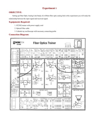
  • 1. Experiment 1 OBJECTIVE: Setting up Fiber Optic Analog Link Study of a 650nm fiber optic analog link in this experiment you will study the relationship between the input signal and received signal. Equipments Required: 1. ST2502 trainer with power supply cord 2. Optical Fiber cable 3. Cathode ray oscilloscope with necessary connecting probe Connection Diagram:
  • 2. Procedure: 1. Connect the power supply cord to the main power plug & to trainer ST2502. 2. Ensure that all switched faults are ‘Off’. 3. Make the following connections as shown in figure 1.1 a. Connect the 1 KHz sine wave output to emitter l's input. b. Connect the Fiber Optics cable between emitter output and detectors input. c. Detector l's output to AC amplifier 1 input. 4. On the board, switch emitter l's driver to analog mode. 5. Switch ON the power supply of trainer and oscilloscope. 6. Observe the input to emitter 1 (TP5) with the output from AC amplifier 1 (TP28) and note that the two signals are same. Questions: 1. What is meant by index profile? 2. What is the drawback of multimode fibers? 3. What is fiber optics?
  • 3. Experiment 2 OBJECTIVE: Setting up Fiber Optic Digital Link Study of a 650 nm fiber optic digital link In this experiment you will study the relationship between the input signal and received signal. Equipments Required 1. ST2502 trainer with power supply cord 2. Optical Fiber cable 3. Cathode ray oscilloscope with necessary connecting probe Connection Diagram:
  • 4. Procedure 1. Connect the power supply cord to the main the Power Supply to the board. 2. Ensure that all switched faults are ‘Off’. 3. Make the following connections as shown in figure 2.1.  Connect the 1 KHz square wave output to emitter l's input.  Connect the fiber optic cable between emitter output and detectors input.  Detector 1's output to comparator 1’s input.  Comparator l's output to AC amplifier l's input 4. On the board, switch emitter 1's driver to digital mode. 5. Switch ON the power supply of trainer and oscilloscope. 6. Monitor both the inputs to comparator 1 (TP13 & 14). Slowly adjust the Comparators bias preset, until DC Level on the input (TP13) lays mid way between the high and low level of the signal on the positive input (TP14). 7. Observe the input to emitter 1 (TP 5) with the output from AC amplifier 1 (TP28) and note that the two signals are same. Questions: 1. Why single mode fibers are used for long distance transmission? 2. What is optical fiber? 3. What is step index profile?
  • 5. Experiment 3 Objective: Study of Intensity Modulation Technique using Analog input signal. To obtain intensity modulation of the analog signal, transmit it over a fiber optic cable and demodulate the same at the receiver and to get back the original signal. Equipments Required: 1. ST2502 trainer with power supply cord 2. Optical Fiber cable 3. Cathode ray oscilloscope with necessary connecting probe Connection Diagram:
  • 6. Procedure: 1. Connect the power supply cord to the main power plug & to trainer ST2502 2. Make the following connections as shown in figure 3.1. a. Connect the FG output marked 1 KHz sine wave to input if emitter 1. b. Plug in a fiber optic link from output of emitter 1 LED to the photo transistor of the detector 1. c. Detector 1 output TP 10 to input of Amplifier TP 27. 3. In the emitter 1 block switch the mode select to analog. 4. Turn the 1 KHz preset in function generator block to fully clockwise (maximum amplitude) position. 5. Switch on the Power Supply of the trainer and oscilloscope. 6. With the help of dual trace oscilloscope observe the input signal at emitter 1 TP 5 also; observe the output from the detector 1. It should carry a smaller version of the original 1 KHz sine wave, illustrating that the modulated light beam has been reconverted back into an electrical signal. 7. The output from detector 1 is further amplified by AC amplifier 1. This amplifier increases the amplitude of the received signal, and also removes the DC component, which is present at detector output. Monitor the output of amplifier 1 TP28 and adjust the gain adjust 1 preset until the monitored signal has same amplitude as that applied to emitter 1 Input TP 5 . 8. While monitoring the output of Amplifier 1 TP 28 change the amplitude of modulating sine wave by varying the 1 KHz preset in the function generator block. Note that as expected, the amplitude of the receiver output signal changes. Questions: a. What is the function of transmitter, optical fiber and receiver? b. Where fiber optics links can be used? c. What is spectral width?
  • 7. Experiment 4 Objective: Study of Intensity Modulation Technique using digital Input signal. The objective of this experiment is to obtain intensity modulation of digital signal, transmit it over fiber optic cable and demodulate the same at the receiver end to get back the original signal. Equipments Required: 1. ST2502 trainer with power supply cord 2. Optical Fiber cable 3. Cathode ray oscilloscope with necessary connecting probe Connection Diagram:
  • 8. Procedure: 1. Connect the power supply cord to the main power plug & to trainer ST2502. 2. Make the following connections as shown in figure 4.1. a. Connect the 1 KHz square wave socket in function generator block to emitter 1 input. b. Connect an optic fiber link between emitter 1 output & Detector 1 input with the help of connector provided. c. Detector output to comparator l's non-inverting (+ve) input. 3. Switch the mode switch in emitter block to digital mode. This ensures that signal applied to the driver's input cause the emitter LED to switch quickly between ‘On’ & ‘Off’ states. 4. Examine the Input to emitter 1 TP 5 on an oscilloscope this 1 KHz square wave is now being used to amplitude modulate emitter I emitter LED. 5. Examine the output of detector 1 TP 10. This should carry a smaller version of original I KHz square wave illustrating that the modulated light beam has been reconverted into an electrical signal. 6. Monitor both input to comparator 1, at TP 13 & 14 and slowly adjust the "Comparator bias 1 preset until the DC Level on the negative input TP 13 lies midway between the high & low level of the signal on the positive input TP. 14. This DC level is comparator's threshold level. 7. Examine the output of comparator 1 TP15 Note that the original digital modulating signal has been reconstructed at the receiver. 8. Once again carefully flex the fiber optic cable we can see that there is no change in output on bending the fiber. The output amplitude is now independent of the bend radius of the cable and that of length of cable, provided that detector output signal is large enough to cross the comparator threshold level. This illustrates one of the advantages of amplitude modulation of a light beam by digital rather than analog means. Also, non-linear ties within the emitter LED & photo transistor causing distortion of the signal at the receiver output are the disadvantages associated with amplitude modulating a light source by analog means. Linearity is not a problem if the light beam is switched ‘On’ & ‘Off’ with a digital signal, since the detector output is simply squared up by a comparator circuit. To overcome problems associated with amplitude modulation of a light beam by analog means, analog signals are often used to vary or modulate some characteristic of a digital signal (e.g. frequency or pulse width.). The digital signal being used to switch the light beam ‘On’ & ‘Off’. The next two experiments illustrate how an analog signal can be used to modulate two specific characteristics of a digital signal. Questions: 1. What is intensity modulation? 2. What is the function of LASER? How the modulated signal is detected?
  • 9. Experiment 5 Objective: The Frequency Modulation System Equipments Required: 1. ST2502 trainer with power supply cord 2. Optical Fiber cable 3. Cathode ray oscilloscope with necessary connecting probe Connection Diagram:
  • 10. Procedure: 1. Connect the power supply cord to the main power plug & to trainer ST2502. 2. Ensure that all switched faults are ‘Off’. 3. Make the following connections as shown in figure 5.1. a) Connect Function generator 1 KHz sine wave signal to frequency modulator input. b) Frequency modulator output TP2 to the emitter 1 input at TP5. c) Connect the optic fiber between the emitter 1 circuit and the detector 1 circuit. d) Detector 1 output TP10 to comparator 1 input at TP14. e) Comparator 1 output TP15 to the PLL detector input at TP23. f) PLL detector output at TP26 to the low pass filter 1 input at TP19 g) Low Pass Filter 1 output TP20 to A C amplifier 1 input at TP27 4. Switch emitter l's driver to digital mode. This ensures that fast changing digital signal applied to the drivers input causes the emitter LED to switch quickly between ‘On’ & ‘Off’ states. 5. Turn the 1 KHz preset in the function generator block to fully anticlockwise (Zero amplitude) position. 6. Switch ON the Power Supply of the trainer and oscilloscope. 7. Monitor the output of the voltage controlled oscillators (VCO) in the frequency modulator block TP2. Note that the frequency of this digital signal is at present constant, since the modulating 1 KHz sine wave has zero amplitude. 8. Examine the output of detector 1 (TP10 and check that the transmitted digital pulses are successfully detected at the receiver). 9. With the help of dual trace oscilloscope monitor both inputs to comparator1. 10. Now adjust the bias 1 preset until the bias input at TP13 is halfway between the top and bottom of the square wave on TP14. You will remember that the function of the comparator is to clean up the square wave after its transmission through the fiber optic link. The output of comparator 1 drives the input of the PLL detector which produces a signal whose average level is proportional to the frequency of the digital stream. This average level is then extracted by low pass filter 1, and amplified by AC Amplifier1 to produce the original analog signal at the amplifiers output TP28. Examine TP28 and note that the output voltage is zero. This is expected since there is currently no modulating voltage in the transmitter. 11. While monitoring the input to the frequency modulator block TP1 and the output from AC amplifier 1 TP28 turn the 1KHz preset to its fully clockwise maximum amplitude) position. Note that the modulating 1 KHz signal now appears at the amplifiers output. If necessary, adjust the amplifiers gain, adjust 1 preset until the two monitored signal are equal in amplitude. 12. In order to fully understand how this frequency modulation transmitter/ receiver system works, examine the inputs and outputs of all functional blocks within the system, using an Oscilloscope. Questions: a) How the FM signal is generated? What are the various detection techniques of FM signals?
  • 11. Experiment 6 Objective: The Pulse Width Modulation System Equipments Required: 1. ST2502 trainer with power supply cord 2. Optical Fiber cable 3. Cathode ray oscilloscope with necessary connecting probe Connection Diagram:
  • 12. Procedure: 1. Connect the power supply cord to the main power plug & to trainer ST2502. 2. Ensure that all switched faults are set to ‘Off’. 3. Make the following connections as shown in figure 6.1. a. FG' s 1KHz sine wave signal to the Pulse width modulator input TP3 b. Pulse width modulator output TP4 to emitter 1 input TP5 c. Connect the optic fiber between the emitter 1 circuit and detector 1 circuit. d. Detector 1 output TP10 to comparator & input at TP14. e. Comparator 1 output TP15 to LPF 1 at TP19. f. LPF 1 output TP20 to A C amplifier 1 input at TP27. 4. Switch emitter 1’s driver to digital mode. This ensures that fast changing digital signals applied to the drivers input because the emitter LED to switch quickly between ‘On’ & ‘Off’ states. 5. Turn the 1 KHz preset of function generator block to fully anticlockwise (zero amplitude) position. 6. Switch ON the Power Supply of the trainer and oscilloscope. 7. Monitor the output of the pulse width modulator block TP4. Note that the pulse width of this digital signal is at present constant, since the modulating 1 KHz sine wave has zero amplitude. 8. Examine the output Detector TP10 and check that the transmitted digital pulse is successfully detected at the receiver. 9. Monitor both inputs’ comparator 1 TP13 & TP14 and if necessary, slowly adjust the comparator's bias preset, until the DC Level on the negative input TP13 lies midway between the high and low level of the signal on the positive input TP14. 10. The average level of comparator l's output is extracted by LPF 1 and then amplified by AC amplifier which also removes the DC offset. Since, the average level of the comparator output is proportional to the pulse width, the original analog signal appears at the amplifiers output TP28. Examine TP28 and note that the output voltage is zero. This is expected since there is currently no modulating voltage at the transmitter. 11. While monitoring the input to the pulse width modulator block TP3 and the output from AC amplifier 1 TP28 turn the 1 KHz preset to its fully clockwise(maximum amplitude position). Note that the modulating 1 KHz signal now appears at the amplifiers output. If necessary, adjust the amplifiers gain adjust 1 preset until the two monitored signals are equal in amplitude. In order to fully understand how this pulse width modulation transmitter/receiver system works, examine the inputs and outputs of all functional blocks within the system using an oscilloscope.
  • 13. Experiment 7 Objective: Study of Propagation Loss in Optical Fiber To measure propagation or attenuation loss in optical fiber Equipments Require: 1. ST2502 trainer with power supply cord 2. Optical Fiber cable 3. Cathode ray oscilloscope with necessary connecting probe Connection Diagram:
  • 14. Procedure: 1. Connect power supply cord to the main power plug & to trainer ST2502. 2. Make the following connections as shown in figure 7.1. a) Function generator’s 1 KHz sine wave output to Input 1 socket of emitter 1 circuit via 4 mm lead. b) Connect 0.5 m optic fiber between emitter 1 output and detector l's input. c) Connect detector 1 output to amplifier 1 input socket via 4mm lead. 3. Switch ON the Power Supply of the trainer and oscilloscope. 4. Set the Oscilloscope channel 1 to 0.5 V / Div and adjust 4 - 6 div amplitude by using X 1 probe with the help of variable pot in function generator block at input 1 of Emitter 1. 5. Observe the output signal from detector TP10 on CRO. 6. Adjust the amplitude of the received signal same as that of transmitted one with the help of gain adjust potentiometer in AC amplifier block. Note this amplitude and name it V1. 7. Now replace the previous FG cable with 1 m cable without disturbing any previous setting. 8. Measure the amplitude at the receiver side again at output of amplifier 1 socket TP 28. Note this value end name it V2. Calculate the propagation (attenuation) loss with the help of following formula. V1 / V2 = e- α (L1 + L2) Where α is loss in nepers / meter 1 neper = 8. 686 dB L 1 = length of shorter cable (0.5 m) L 2 = Length of longer cable (1 m) Questions: 1. How to measure propagation losses? 2. By what optical cable is made up of? 3. What is step index fibre?
  • 15. Experiment 8 Objective: Study of Bending Loss The object of this experiment into study bending loss Equipments Required: 1. ST2502 trainer with power supply cord 2. Optical Faber cable 3. Cathode ray oscilloscope with necessary connecting probe 4. Mandrel Connection Diagram:
  • 16. Procedure: 1. Connect power supply cord to the main power plug & to trainer ST2502 . 2. Make the connections as shown in figure 8.1. a) Function Generator 1 KHz sine wave output to input socket of emitter Circuit via 4 mm lead. b) Connect 0.5 m optic fiber between emitter output and detectors input. c) Connect Detector output to amplifier input socket via 4mm lead. 3. Switch ‘On’ the power supply of the trainer and oscilloscope. 4. Set the Oscilloscope channel 1 to 0.5 V/ Div and adjust 4-6 div amplitude by using X 1 probe with the help of variable pot in function generator Block at input of Emitter. 5. Observe the output signal from detector (TP8) on CRO. 6. Adjust the amplitude of the received signal as that of transmitted one with the help of gain adjusts potentiometer in AC amplifier block. Note this amplitude and name it V 1 . 7. Wind the fiber optic cable on the mandrel and observe the corresponding AC amplifier output on CRO, it will be gradually reducing, showing loss due to bends. Questions: 1. What is the reason of bending losses? 2. What is core and cladding? 3. What is the function of cladding?
  • 17. Experiment 9 Objective: Measurement of Optical Power using Optical Power Meter To measure optical power using optical power meter. Equipments Required: 1. ST2502 trainer with power supply cord 2. Optical Fabre cable 3. Cathode ray oscilloscope with necessary connecting probe 4. Power Meter ST2551 with power supply cord Connection Diagram:
  • 18. Procedure: 1. Connect the Power supply cord to mains supply and to the trainer ST2502. 2. Ensure that all switched faults are ‘Off’. 3. Connect the fiber optic cable between emitters 1's output & power meter's input. 4. On the board, switch emitter l's driver to analog mode. Keep the power meter's wavelength selector switch in 60 nm 5. Switch ON the power supply of the trainer and power meter. 6. Note the reading displayed in power meter. 7. Switch the wavelength selector switch to 950 nm positions. & note the reading displayed on power meter. 8. Perform the same experiment with emitter 2. Questions: 1. How the power is measured using power meter? 2. What is wavelength of light? 3. What do you understand by fiber bending?
  • 19. Experiment 10 Objective: Measurement of propagation loss using Optical Power Meter To measure propagation loss in optical fiber using optical power meter. Equipments Required: 1. ST2502 trainer with power supply cord 2. Optical fiber cable 3. Cathode ray oscilloscope with necessary connecting probe 4. Power Meter ST2551 with power supply cord Connection Diagram:
  • 20. Procedure: 1. Connect the Power supply cord to mains supply and to the trainer ST2501. 2. Keep the mode switch in emitter 1 circuit in analog mode 3. Connect the 0.5m fiber cable in between the emitter LED & I/P of power meter. 4. Switch on the instrument fiber optic trainer & power meter (Keep the wavelength switch in 660 nm, position). Note the reading in power meter. 5. Replace the 0.5m fiber cable with the 1m cables without disturbing any setting. 6. Again note the reading in power. This reading will be lesser then the previous one, indicating that the ropagation loss increases with increase in length. 7. Perform the same experiment with emitter 2. Questions: 1. How Propagation Loss in optical fiber is measured? 2. What are the various types of losses in fiber? 3. What is the formula used for measurement of losses?
  • 21. Experiment 11 Objective: 1. Measurement of Numerical Aperture 2. Measurement of the Numerical Aperture (NA) of the fiber Equipments Required: 1. ST2502 trainer with power supply cord 2. Optical Fibre cable 3. Numerical Aperture measurement Jig Connection Diagram:
  • 22. Procedure: 1. Connect the Power supply cord to mains supply and to the trainer ST2502. 2. Connect the frequency generator's 1 KHz sine wave output to input of emitter 1 circuit. Adjust its amplitude at 5Vpp. 3. Connect one end of fiber cable to the output socket of emitter 1 circuit and the other end to the numerical aperture measurement jig. Hold the white screen facing the fiber such that its cut face is perpendicular to the axis of the fiber. 4. Hold the white screen with 4 concentric circles (10, 15, 20 & 25mm diameter) vertically at a suitable distance to make the red spot from the fiber coincide with 10 mm circle. 5. Record the distance of screen from the fiber end L and note the diameter W of the spot. Compute the numerical aperture from the formula given below W NA = -------------- = sin max 4L2 + W2 6. Vary the distance between in screen and fiber optic cable and make it coincide with one of the concentric circles. 7. Note its distance. 8. Tabulate the various distances and diameter of the circles made on the white screen and computes the numerical aperture from the formula given above. Inferences: The N.A. recorded in the manufacturer's data sheet is 0.5. The variation in the observation is due to fiber being used. The Acceptance Angle is given by 2sinθmax. The deviation from the data sheet is again due to fiber being used. Questions What is numerical aperture? Write the formula for numerical aperture? What is the significance of numerical aperture?
  • 23. Experiment 12 Objective: Characteristics of E-O Converter using OPM Study of characteristics of E-O converter using OPM Equipments Required: 1. ST2502 Trainer with power supply cord 2. Optical Fiber cable 3. Cathode ray oscilloscope with necessary connecting probe 4. Power Meter ST 2551 with power supply cord Connection Diagram:
  • 24. Procedure: 1. Connect the Power supply cord to mains supply and to the trainer ST2502. 2. Ensure that all switched faults are ‘Off’. 3. Put emitter 1 block in digital mode. Connect the bias 1 on comparator 1 block preset TP13 to the emitter 1 I/P at TP5. 4. Adjust the bias l preset to its minimum setting fully counter clockwise. Connect the Fiber Optics cable between the emitter 1 LED & power meter. 5. Switch ON the power supply of the trainer and oscilloscope. 6. Note down the reading from power meter. 7. Vary the bias preset so as to vary the voltage applied to emitter 1 LED. 8. Record the change in power meter reading corresponding to change in forward voltage. Plot the graph between forward voltage and power meter reading. 9. Perform the experiment with emitter 2. Questions: 1. What is the function of optical power meter? 2. What is the full form of LED? 3. Why LED is not used for long distance transmission?
  • 25. Experiment 13 Objective: Characteristics of E - O Converter The aim of this experiment is to plot the characteristic of LED. Equipments Required: 1. ST2502 trainer with power supply cord 2. Optical Fibre cable 3. Cathode ray oscilloscope with necessary connecting probe Connection Diagram:
  • 26. Procedure: 1. Connect the Power supply cord to mains supply and to the trainer ST2502. 2. Ensure that all switched faults are in ‘Off’ condition. 3. Put emitter 1 block in Digital Mode 4. Make connections as shown in figure 13.1 a) Connect the bias 1 preset on comparator 1 (TP13) to the emitter 1 input at (TP5) b) Adjust the bias 1 preset to its minimum setting fully counter clockwise. c) Now look down the emitter 1 LED Socket and slowly advance the setting of the bias 1 preset until in subdued lighting the light from LED is just visible. 5. Connect the DMM between + 12V supply and TP6, the cathode of LED. The DMM will now read the forward voltage (V f) Measure the voltage drop across the 1K (R9) current limiting resistors by connecting DMM between TP6 and TP38. The forward current is given by dividing the readings by 1K. This If is known as threshold current. DVM reading ------------------- mA 1000 6. Vary the bias 1 preset so as to vary the forward voltage (as 1.3, 1.4…1.7), note the corresponding If (forward current). 7. Record these values of Vf and If and plot the characteristic between these two. Questions: 1. What are the characteristics of fiber optics link? 2. What is the function of transmitter? 3. How light signals are converted back to the electrical signals?
  • 27. Experiment 14 Objective: Characteristics of Fiber Optics communication Link The aim of experiment is to study the Vin (AC) versus Vo (AC). Equipments Required: 1. ST2502 trainer with power supply cord 2. Optical Fiber cable 3. Cathode ray oscilloscope with necessary connecting probe Connection Diagram:
  • 28. Procedure: 1. Connect the Power supply cord to mains supply and to the trainer ST2502. 2. Make the following connections as shown in figure 14.1. a. Function generator 1 KHz sine wave output to input socket of emitter 1 circuit via 4mm lead. b. Connect optic fiber between emitter l’s output and detector 1’s input. c. Connect Detector 1 output to amplifier 1 input socket via 4nm lead. 3. Switch on the Power Supply. 4. Set the amplitude of the function generator to 2V p-p. 5. Observe the transmitted and received signal on CRO. Vo (output voltage) should be in the same order as Vin (input voltage). 6. Next set Vin to suitable values and note the values of Vo. 7. Tabulate and plot a graph Vo versus Vin & compute Vo/Vin. Questions: 1. What is the advantage of amplitude modulation in terms of bandwidth requirement? 2. How amplitude modulation signal is generated? 3. What is the detection process amplitude modulated signals?
  • 29. Experiment 15 Objective: 1. Setting up of Fiber Optics voice link using Intensity Modulation 2. Study of voice communication through Fiber Optic cable using amplitude modulation Equipments Required: 1. ST2502 trainer with power supply cord 2. Optical Fiber cable 3. Cathode ray oscilloscope with necessary connecting probe Connection Diagram:
  • 30. Procedure: 1. Connect the power supply cord to the main power plug & to trainer ST2502. 2. Make the following connections as shown in figure 15.1. a. Connect the FG output marked 1 KHz sine wave to input if emitter 1. b. Plug in a fiber optic link from output of emitter 1 LED to the photo transistor of the detector 1. 3. Detector 1 output TP 10 to input of Amplifier TP 27. 4. In the emitter 1 block switch the mode select to analog. 5. Turn the 1 KHz preset in function generator block to fully clockwise (maximum amplitude) position. 6. Switch ON the Power Supply of the trainer and oscilloscope. 7. With the help of dual trace oscilloscope observe the input signal at emitter 1 TP 5 also; observe the output from the detector 1. It should carry a smaller version of the original 1 KHz sine wave, illustrating that the modulated light beam has been reconverted back into an electrical signal. 8. The output from detector 1 is further amplified by AC amplifier 1. This amplifier increases the amplitude of the received signal, and also removes the DC component, which is present at detector output. Monitor the output of 9. amplifier 1 TP28 and adjust the gain adjust 1 preset until the monitored signal has same amplitude as that applied to emitter 1 Input TP 5 . 10. While monitoring the output of Amplifier 1 TP 28 change the amplitude of modulating sine wave by varying the 1 KHz preset in the function generator block. Note that as expected, the amplitude of the receiver output signal changes. 11. Disconnect the emitter 1’s input to 1 KHz sine wave socket. 12. Make the following additional connections (as shown in figure 15.1). 13. Audio input block's input to microphone. 14. Connect the output of audio input block to emitter l’s input. 15. AC Amplifier's output to input of audio output block. 16. Observe that same audio output is available on the speaker as fed to the microphone. Questions: 1. What is the drawback of FM modulation in terms of bandwidth requirement? 2. How the FM signals are generated? 3. What is the function of AC amplifier?
  • 31. Experiment 16 Objective: Setting up Fiber Optics voice link using Frequency Modulation The objective of this experiment is to demonstrate voice transmission through optic fiber using F M. Equipments Required: 1. ST2502 trainer with power supply cord 2. Optical Fiber cable 3. Cathode ray oscilloscope with necessary connecting probe Connection Diagram:
  • 32. Procedure: 1. Connect the power supply cord to the main power plug & to trainer ST2502. 2. Ensure that all switched faults are ‘Off’. 3. Make the following connections as shown in figure 16.1. a. Connect Function generator 1 KHz sine wave signal to frequency modulator input. b. Frequency modulator output TP2 to the emitter 1 input at TP5. c. Connect the optic fiber between the emitter 1 circuit and the detector 1 circuit. d. Detector 1 output TP10 to comparator 1 input at TP14. e. Comparator 1 output TP15 to the PLL detector input at TP23. f. PLL detector output at TP26 to the low pass filter 1 input at TP19 g. Low Pass Filter 1 output TP20 to A C amplifier 1 input at TP27 4. Switch emitter l's driver to digital mode. This ensures that fast changing digital signal applied to the drivers input causes the emitter LED to switch quickly between ‘On’ & ‘Off’ states. 5. Turn the 1 KHz preset in the function generator block to fully anticlockwise (Zero amplitude) position. 6. Disconnect the 1 KHz sine wave output from in put of F M block. 7. Make the following additional connections as shown in figure 16.1 without disturbing previous setting. 8. Plug the Microphone in the input of Audio input block. 9. Output of Audio input block to input of FM block. 10. Output of AC Amp block to the Power Supply. 11. Speak in the Microphone and listen the same in the speaker / Headphone. Questions: 1. What is the drawback of FM modulation in terms of bandwidth requirement? 2. How the FM signals are generated? 3. What is the function of AC amplifier?
  • 33. Experiment 17 Objective: Setting up of Fiber Optic Voice Link using PWM Study of voice transmission through Fiber Optic cable using PWM Equipments Required: ST2502 trainer with power supply cord Optical Fiber cable Cathode ray oscilloscope with necessary connecting probe Connection Diagram:
  • 34. Procedure: 1. Connect the power supply cord to the main power plug & to trainer ST2502. 2. Ensure that all switched faults are set to ‘Off’. 3. Make the following connections as shown in figure 17.1. i. FG' s 1KHz sine wave signal to the Pulse width modulator input TP3 ii. Pulse width modulator output TP4 to emitter 1 input TP5 iii. Connect the optic fiber between the emitter 1 circuit and detector 1 circuit. iv. Detector 1 output TP10 to comparator & input at TP14. v. Comparator 1 output TP15 to LPF 1 at TP19. vi. LPF 1 output TP20 to A C amplifier 1 input at TP27. 4. Switch emitter 1’s driver to digital mode. This ensures that fast changing digital signals applied to the drivers input because the emitter LED to switch quickly between ‘On’ & ‘Off’ states. 5. Turn the 1 KHz preset of function generator block to fully anticlockwise (zero amplitude) position. 6. Switch on the Power Supply of the trainer and oscilloscope. 7. Monitor the output of the pulse width modulator block TP4. Note that the pulse width of this digital signal is at present constant, since the modulating 1 KHz sine wave has zero amplitude. 8. Examine the output Detector TP10 and check that the transmitted digital pulse is successfully detected at the receiver. 9. Monitor both inputs’ comparator 1 TP13 & TP14 and if necessary, slowly adjust the comparator's bias preset, until the DC Level on the negative input TP13 lies midway between the high and low level of the signal on the positive input TP14. 10. The average level of comparator l's output is extracted by LPF 1 and then amplified by AC amplifier which also removes the DC offset. Since, the average level of the comparator output is proportional to the pulse width, the original analog signal appears at the amplifiers output TP28. Examine TP28 and note that the output voltage is zero. This is expected since there is currently no modulating voltage at the transmitter. 11. While monitoring the input to the pulse width modulator block TP3 and the output from AC amplifier 1 TP28 turn the 1 KHz preset to its fully clockwise (maximum amplitude position). Note that the modulating 1 KHz signal now appears at the amplifiers output. If necessary, adjust the amplifiers gain adjust 1 preset until the two monitored signals are equal in amplitude. In order to fully understand how this pulse width modulation transmitter/ receiver system works, examine the inputs and outputs of all functional blocks 12. within the system using an oscilloscope. 13. Disconnect the PWM input from 1 KHz sine wave socket 14. Make the following additional connection (as shown in figure 17.1) without disturbing any previous settings
  • 35. a) Plug the microphone into input of audio input block b) Output of audio input block to input of PWM block c) Output of AC Amp block to input of audio output block 15. Observe that the same audio sound is available in the speaker as fed to microphone. Questions: 1. What is frequency band for voice signals? 2. By what means the voice signals are converted into electrical signals? 3. Why PWM method is generally preferred for communication system?
  • 36. Experiment 18 Objective: Study of Switched Fault in Intensity Mode Study of the effect of switched fault number 1& 5 on amplitude modulated system Equipments Required: 1. 2. 3.
  • 37. ST2502 trainer with power supply cord Optical Fiber cable Cathode ray oscilloscope with necessary connecting probe Connection Diagram:
  • 38.
  • 40. Connect the power supply cord to the main power plug & to trainer ST2502 . Make the following connections as shown in figure 18.1. a. b. c.
  • 41. Connect the FG output marked 1 KHz sine wave to input if emitter 1. Plug in a fiber optic link from output of emitter 1 LED to the photo transistor of the detector 1. Detector 1 output TP 10 to input of Amplifier TP 27. 3. 4. 5. 6. 7. 8. 9. 10. 11. 12.
  • 42. Switch ON the Power Supply of the trainer and oscilloscope. See that AM System is operating correctly. Adjust the gain adjust potentiometer in the AC amplifier circuit to provide a sinusoidal signal of same amplitude as input. Switch on fault 1. All other faults are set to ‘Off’. This fault removes the bias normally present on emitter 1's LED in analog mode so that distortion occurs when analog amplitude modulation takes place. Turn ‘Off’ the fault 1 and check that A.M. system is operating correctly. Adjust the preset to provide a sinusoidal signal of 4 V peak to peak at the output. Switch ‘On’ fault 5. This shorts the output and negative input of AC amplifier 2. So that amplifier gain is always +1, irrespective of the position of the gain adjust 2 preset. Observe the output, and vary the gain adjust preset. Is there any change in output? Switch fault 5 ‘Off’. Switch Power Supply ‘Off’. Questions: 1. 2. 3.
  • 43. What do you mean by intensity modulation? What is the significance of switch fault? Which type of optical source is used for intensity modulation? Scientech Technologies Pvt. Ltd.
  • 44. 83
  • 45. ST2502 Experiment 19 Objective: Study of switched Faults in FM System To study the Effect of fault number 4, 6, & 8 in F.M. System Equipments Required: 1. 2. 3.
  • 46. ST2502 trainer with power supply cord Optical Fiber cable Cathode ray oscilloscope with necessary connecting probe Connection Diagram:
  • 47. Figure 19.1 Scientech Technologies Pvt. Ltd.
  • 48. 84
  • 50. Connect the power supply cord to the main power plug & to trainer ST2502. Ensure that all switched faults are ‘Off’. Make the following connections as shown in figure 19.1. a. b. c. d. e. f. g.
  • 51. Connect Function generator 1 KHz sine wave signal to frequency modulator input. Frequency modulator output TP2 to the emitter 1 input at TP5. Connect the optic fiber between the emitter 1 circuit and the detector 1 circuit. Detector 1 output TP10 to comparator 1 input at TP14. Comparator 1 output TP15 to the PLL detector input at TP23. PLL detector output at TP26 to the low pass filter 1 input at TP19 Low Pass Filter 1 output TP20 to A C amplifier 1 input at TP27 4. 5. 6. 7. 8. 9. 10. 11. 12. 13. 14. 15. 16.
  • 52. Set the emitter 1 to digital mode. Switch ON the power supply of the trainer and oscilloscope. Check, that FM System is operating correctly. Adjust the preset in AC amplifier block to give a sinusoidal signal of amplitude same as input. Switch fault 4 ‘On’ all other faults set to ‘Off’. This fault affects the phase locked loop detector between the voltage controlled oscillator (VCO) and phase comparator (exclusive OR gate). The result is that the PLL no longer follows changes in the frequency of the input signal. Observe the system output at TP 28 and the output of PLL block. Switch fault 4 ‘Off’. Switch fault 6 ‘On’. This changes the DC bias on frequency modulator VCO input from +2.5V to 0V, So that the VCO no longer oscillates irrespective of the signal applied to its input. Observe the system output and the FM block's output. Switch fault 6 ‘Off’. Switch fault 8 ‘On’. These shorts pin 11 'R' of IC9 to junction of R90 &C32. Observe the output of system and also PLL output. Switch ‘Off’ fault 8 and check the operation of FM System. Scientech Technologies Pvt. Ltd.
  • 53. 85
  • 55. What is the function of VCO? What is FM? What is the function of PLL while detecting the transmitted signals?
  • 57.
  • 58. 86
  • 59. ST2502 Experiment 20 Objective: Study of switched Faults in PWM System To study the Effect of Switched Faults 2, 3 & 7 on pulse width modulation system. Equipments Required: 1. 2. 3.
  • 60. ST2502 trainer with power supply cord Optical Fiber cable Cathode ray oscilloscope with necessary connecting probe Connection Diagram:
  • 61. Figure 20.1 Scientech Technologies Pvt. Ltd.
  • 62. 87
  • 64. Connect Power Supply cord to the mains and to the trainer ST2502. Ensure that all switched faults are set to ‘Off’. Make the following connections as shown in figure 20.1. a. b. c. d. e. f.
  • 65. FG' s 1KHz sine wave signal to the Pulse width modulator input TP3 Pulse width modulator output TP4 to emitter 1 input TP5 Connect the optic fiber between the emitter 1 circuit and detector 1 circuit. Detector 1 output TP10 to comparator & input at TP14. Comparator 1 output TP15 to LPF 1 at TP19. LPF 1 output TP20 to A C amplifier 1 input at TP27. 4. 5. 6. 7. 8. 9. 10. 11. 12. 13. 14. 15.
  • 66. Switch on the Power Supply of the trainer and oscilloscope. Switch on the Power Supply. Check the correct operation of the PWM system. Switch on fault number 2. This open circuits the feed back loop of the first stage of detector 2's voltage amplifier, so that the final amplifier output at TP 28 saturates. Observe the output at detector 2 it saturates at + 10V, and observe the system output, it goes to zero. Try to the explain reason behind it. Switch fault 2 ‘Off’. Switch on fault number 3. This open circuits the positive. In put of first comparator and due to this the system output goes zero. Try to explain reason behind it. Switch ‘Off’ fault 3. Switch fault 7 ‘On’. This switches ‘Off’ constant current source to PWM so that output level of modulator is permanently high. Observe the output of PWM, it goes permanently high and output of system to zero. Try explaining reasons for it. Switch off fault 7 check correct operation of PWM System. Questions: 1. 2. 3.
  • 67. What is the significance of Switched Faults? What is full form of PWM? What is the function of PWM? Scientech Technologies Pvt. Ltd.
  • 68. 88
  • 69. ST2502 Experiment 21 Objective: Computer to Computer communication using RS232 interface via Fiber Optic Link There are 2 fibers optic Links provided on fiber optic trainer. We shall utilize these two links to communicate from one PC to other & via-versa. That means it is a Duplex system of communication using fiber optic link. The Software developed will help to transmit & receive messages from the computers. Equipments Required: 1. 2. 3. 4.
  • 70. ST2502 trainer with power supply cord Optical Fiber cable Personal computer - 2 Nos. 486 or Pentium, DOS 6.0 or onwards, CD drive RS232 cables for connecting PC's to Trainer - 2 Nos. Connection Diagram:
  • 71. Figure 21.1 Scientech Technologies Pvt. Ltd.
  • 72. 89
  • 74. Keep one PC towards left and another towards right of fiber optic trainer. Load the software in PC 1 & PC2, with the help of the CD supplied. Keep one of the COM port free on each of PC to connect the RS232 cables. Keep baud rate of both PC equal, say 57600. Switch off both the PC's. Make the following connections on the fiber optic trainer. a. b. c. d. e. f. g. h. i. j. k. l.
  • 75. Connect Fiber Link on CHI (emitter to Detector). Connect Fiber Link on CH2 (emitter to Detector). Connect output of Detector 1 to comparator 1 input. Connect output of Detector 2 to comparator 2 inputs. Connect 1 KHz square wave to input of CHI (emitter). Keep mode switch of both channels to digital and all Switched Faults in ‘Off’ position. Switch on the Trainer. Observe input to emitter 1 and output of comparator 1. Adjust bias of comparator 1 for square wave output. Switch 1 KHz square wave from the input of CHI to input of CH2 (emitter) and adjust comparator 2 bias for square wave output. Switch off the Trainer. Make connections as shown in diagram 17 and Switch on the Trainer. Fiber optic trainer is ready for connection to PC's. Switch off the trainer. Connect PC1 & PC2 to D type connectors. (Any to anyone) switch on the PC's and the Trainer & start working. Whatever you type in PC1 will be seen on the transmit column of PC1 and will also be received in the receive column of PC2 simultaneously & vice versa. Remove any of the fiber links. To transmit & receive of that link is disconnected. m. Change baud rate of any of the PCs & you will find that data is not transmitted. Keep the baud rate same. n.
  • 76. Reduce the baud rate of both the PCs & you will see that transmit rate is lower. Switch off the Trainer and the PCs. Questions: 1. 2. 3.
  • 77. What RS 232C stands for? What is the pin configuration for 25 pin D connector? What is the pin configuration for 9 pin D connector? Scientech Technologies Pvt. Ltd.
  • 78. 90
  • 79. ST2502 Experiment 22 Objective: Bit Rate Measurement Determining the bit rate supported by the fiber optic link Equipments Required: 1. 2. 3.
  • 80. ST2502 trainer with power supply cord Optical Fiber cable Oscilloscope with power supply cord Procedure: 1. 2. 3. 4. 5. 6.
  • 81. Set up the fiber optic digital link as explained earlier, and ensure that the link is working satisfactorily. Remove the on board TTL output from the emitter input and connect the TTL output of square wave generator to emitter input. Keep the frequency at 10 KHz. Observe the received output on the oscilloscope. Vary the frequency of the TTL input observing the output each time (You can adjust the comparator's bias preset). Note the frequency at which the output is distorted or reduces to zero. The bit rate supported by the link is twice the frequency reading corresponding to zero/distorted output in bits per second. Questions: 1. 2.
  • 82. How to determine the bit rate? What is optical fiber link? Scientech Technologies Pvt. Ltd.
  • 83. 91
  • 84. ST2502 Experiment 23 Objective: Sensitivity Determining the sensitivity of the Fiber Optic Link Procedure: Sensitivity is defined as the minimum power incident on the photo detector in order to establish the link. 1. 2. 3. 4. 5. 6. 7.
  • 85. 8.
  • 86. Set up the fiber optic digital link as explained earlier using 0.5m cable, and ensure that the link is working satisfactorily. Remove the on board TTL output from the emitter input and connect the output of square wave generator to emitter input. Observe the output of the detector on the oscilloscope. Remove the end of the fiber connected to the detector and connects it to the optical power meter. Note the reading on the power meter Po. This reading is the power being transmitted to the receiver from the source. Remove the fiber end which is connected to the power meter and connect it back to receiver. Slowly reduce the amplitude of the square wave till the output being viewed on the oscilloscope reduces to zero. Remove the fiber end from the receiver and connect it to the power meter. Note the reading on the power meter Ps. This gives the measure of sensitivity of the receiver. Questions: 1. 2.
  • 87. Define the sensitivity? What are the elements of fiber optics link? Scientech Technologies Pvt. Ltd.
  • 88. 92
  • 89. ST2502 Experiment 24 Objective: Power Budget The Power margin is defined by: Po-Pi-Ps Where, Po is the power transmitted Pi is the power lost in the fiber Ps the sensitivity of the receiver Procedure: 1. 2. 3.
  • 90. Assuming that the power lost in the 0.5m fiber Pi is negligible, Po -Ps gives power margin of the link. Repeat the sensitivity experiment with 1 m fiber optic cable. In this case calculate the Pi as follows: Connect the 1m fiber to the source and power meter. Note the power meter reading. We call it p1. Assuming that the power lost in the 0.5m fiber is negligible, Pi- is P1- Po. Po-Pi-Ps is the power margin for this link. Questions: 1. 2.
  • 91. How to determine power Margin? What do you understand by power budget?