1. D. Prasanna Kumari, R. Surya Prakasha Rao, B. Vijaya Bhaskar / International Journal of
Engineering Research and Applications (IJERA) ISSN: 2248-9622 www.ijera.com
Vol. 2, Issue4, July-August 2012, pp.2177-2180
A Future Technology For Enhanced Operation In Flip-Flop
Oriented Circuits
D. PRASANNA KUMARI, R. SURYA PRAKASHA RAO, B. VIJAYA
BHASKAR
Department of ECE, St. Theresa College of Engg. and Tech., Andhra Pradesh, India
Assistant Professor, Department of ECE, St. Theresa College of Engg. and Tech., Andhra Pradesh, India
Associate Professor, Department of ECE, St. Theresa College of Engg. and Tech., Andhra Pradesh, India
ABSTRACT
In this paper a new technique is Flip-flops can be either simple (transparent or
proposed based on the comparison between opaque) or clocked (synchronous or edge-
Conventional Transistorized Flip-flop and Data triggered); the simple ones are commonly called
transition Look ahead D flip flop here we are latches. The word latch is mainly used for storage
checking the working of DLDFF and the elements, while clocked devices are described as
conventional D Flip-flop after that we are flip-flops
analyzing the characteristic comparison using
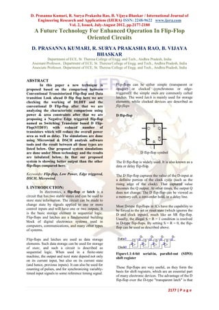
power & area constraints after that we are D flip-flop
proposing a Negative Edge triggered flip-flop
named as Switching Transistor based D Flip-
Flop(STDFF) with reduced number of
transistors which will reduce the overall power
area as well as delay. The simulations are done
using Microwind & DSCH analysis software
tools and the result between all those types are
listed below. Our proposed system simulations
are done under 50nm technology and the results D flip-flop symbol
are tabulated below. In that our proposed
system is showing better output than the other The D flip-flop is widely used. It is also known as a
flip-flops compared here. data or delay flip-flop.
Keywords: Flip-flop, Low Power, Edge triggered, The D flip-flop captures the value of the D-input at
DSCH, Microwind. a definite portion of the clock cycle (such as the
rising edge of the clock). That captured value
I. INTRODUCTION: becomes the Q output. At other times, the output Q
In electronics, a flip-flop or latch is a does not change. The D flip-flop can be viewed as
circuit that has two stable states and can be used to a memory cell, a zero-order hold, or a delay line.
store state information. The circuit can be made to
change state by signals applied to one or more Most D-type flip-flops in ICs have the capability to
control inputs and will have one or two outputs. It be forced to the set or reset state (which ignores the
is the basic storage element in sequential logic. D and clock inputs), much like an SR flip-flop.
Flip-flops and latches are a fundamental building Usually, the illegal S = R = 1 condition is resolved
block of digital electronics systems used in in D-type flip-flops. By setting S = R = 0, the flip-
computers, communications, and many other types flop can be used as described above.
of systems.
Flip-flops and latches are used as data storage
elements. Such data storage can be used for storage
of state, and such a circuit is described as
sequential logic. When used in a finite-state Figure1.1:4-bit serial-in, parallel-out (SIPO)
machine, the output and next state depend not only shift register
on its current input, but also on its current state
(and hence, previous inputs). It can also be used for
counting of pulses, and for synchronizing variably- These flip-flops are very useful, as they form the
basis for shift registers, which are an essential part
timed input signals to some reference timing signal.
of many electronic devices. The advantage of the D
flip-flop over the D-type "transparent latch" is that
2177 | P a g e
2. D. Prasanna Kumari, R. Surya Prakasha Rao, B. Vijaya Bhaskar / International Journal of
Engineering Research and Applications (IJERA) ISSN: 2248-9622 www.ijera.com
Vol. 2, Issue4, July-August 2012, pp.2177-2180
the signal on the D input pin is captured the classified as synchronous and asynchronous
moment the flip-flop is clocked, and subsequent counters based on the application of clock to the
changes on the D input will be ignored until the flip-flops. A synchronous counter is clocked by a
next clock event. An exception is that some flip- single clock for
flops have a "reset" signal input, which will reset Q all the stages and the output for each stage changes
(to zero), and may be either asynchronous or at the same time.
synchronous with the clock. .
The above circuit shifts the contents of the register
to the right, one bit position on each active
transition of the clock. The input X is shifted into
the leftmost bit position.
Types of D Flip-Flops
a. Classical Negative-edge-triggered D flip-
flop
b. Master–slave pulse-triggered D flip-flop
c. Edge-triggered dynamic D storage
element
Figure.3: Data transition Look ahead D Flip-
a. Conventional Low Power D Flip-flop Flop
Flip-Flops are the basic elements for
storing information and they are the fundamental I. Our Proposed Negative Edge Triggered
building blocks for all sequential circuits. Flip- Flip-Flop Design (STDFF)
flops, have their content change only either at the Edge-triggered flip-flops are becoming a
rising or falling edge of the enable signal. But, after popular technique for low-power designs since they
the rising or falling edge of the enable signal, the effectively enable a halving of the clock frequency.
flip-flop’s content remains constant even if the A dual pulse clock generator is needed to generate
input changes. In a conventional D Flip Flop shown pulses at both rising and falling edges of a low-
in Figure 2, the clock signal always flows into the swing clock. This Particular clock pulse is used to
D flip-flop irrespective of whether the input switch the ground of the flip-flop circuit. This
changes or not. Part of the clock energy is ground will be utilized by the NMOS and PMOS
consumed by the internal clock buffer to control connected directly to the D input of the circuit. The
the transmission gates unnecessarily. Hence, if the Proposed system is shown in the figure below.
input of the flip-flop is identical to its output, the
switching of the clock can be suppressed to
conserve power.
Figure.4: Our Proposed Negative Edge
Triggered flip-flop
By using the Transistor switching logic
Figure.2: Conventional D Flip-flop Design only we are designing this circuit so it will be
DLDFF consuming only less power when compared to all
other circuits. As well as we are having only 8
In a DLDFF shown in Figure 3, the gating Transistors including the not gates also. So we will
function is derived within the flip flop without any be having much reduced power and area when
external control signal. The external clock signal of compared to the other two designs. At the same
the flip-flop still switches. But, the clock signal time due to the reduced no of transistor count we
flowing into the flip flop is deactivated when there can reduce the delay oriented things also. Thus we
are no data transitions. Generally flip- flop finds its are reducing the overall switching delay and power,
best application in the counters. Counters can be area consumption.
2178 | P a g e
3. D. Prasanna Kumari, R. Surya Prakasha Rao, B. Vijaya Bhaskar / International Journal of
Engineering Research and Applications (IJERA) ISSN: 2248-9622 www.ijera.com
Vol. 2, Issue4, July-August 2012, pp.2177-2180
Figure.5: Waveform Output of the Proposed
Negative Edge Triggered flip-flop
The graph represents the input & output
characteristics of our proposed system from that we
can clearly understand how it works as negative
edge triggered flip-flop. There is some nano
seconds delay is there even though it’s a negligible
amount only. Those delays can be further reduced
by reducing the sizes of the transistor we are using
in this circuit. Or by reducing the nano meter Figure.6: Layout of the Proposed Design
technology also we can reduce the constraints. The
Layout design of the proposed new flip-flop is
shown in the figure6 the area of that is mentioned
at the downside of the layout. The Power
consumption characteristics also mentioned below
in figure7.
Figure7: Power Characteristic of the Proposed Design
II. Tabulation
Power & Area Comparison Table
Type Power Area
Consumption Consumption
Conventional D Flip-Flop 1.686uW 252um2
DLDFF 2.634uW 270um2
Our Proposed 0.384uW 162um2
Design(STDFF)
2179 | P a g e
4. D. Prasanna Kumari, R. Surya Prakasha Rao, B. Vijaya Bhaskar / International Journal of
Engineering Research and Applications (IJERA) ISSN: 2248-9622 www.ijera.com
Vol. 2, Issue4, July-August 2012, pp.2177-2180
Thus the Proposed Switching Transistor Based D embedded logic,” in Symp. VLSI Circuits, Dig.
Flip-flop design shows much less power & Area Tech. Papers, Jun. 1998, pp. 108–109.
constraints than the Existing two Flip-Flop designs. [12] D. Markovic, B. Nikolic, and R. Brodersen,
“Analysis and design of low-energy flip-flops,” in
Proc. Int. Symp. Low Power Electron.
III. CONCLUSION: Des.,Huntington Beach, CA, Aug. 2001, pp. 52–
In this Paper we proposed a new D flip 55.
flop design which is named as Switching Transistor [13] J. Tschanz, Y. Ye, L. Wei, V. Govindarajulu, N.
Based D Flip Flop (STDFF). The Proposed system Borkar, S. Burns, T. Karnik, S. Borkar, and V.
shows 85% Power improvement than the Existing De, “Design optimizations of a high performance
Data Transition look ahead D Flip-Flop and it microprocessor using combinations of dual-Vt
shows an improvement of 40% in area constraints. allocation and transistor sizing,” in IEEE Symp.
Thus our proposed system is having very less VLSI Circuits, Dig. Tech. Papers, Jun. 2002, pp.
218–219.
power and area constraints which will lead to [14] J. Rabaey, A. Chandrakasan, and B. Nikolic,
improvement in the case implementation in future Digital Integrated Circuits. Englewood Cliffs,
mobile devices. This can be much suitable for NJ: Prentice-Hall, 2003.
application of battery oriented operation for less [15] Shigematsu, S. Mutoh, Y. Matsuya, Y. Tanabe,
power and area. In future we can add some other and J. Yamada, “A 1-V high-speed MTCMOS
leakage reduction techniques and the power can be circuit scheme for power-down application
further reduced. circuits,” IEEE J. Solid-State Circuits, vol. 32,
no. 6, pp. 861–869, Jun. 1997.
[16] T. Sakurai, “Low –power CMOS design through
VII. REFERENCE: Vth control and lowswing circuits,” in Proc.
[1] M. Nogawa and Y.Ohtomo, “A Data-Transition ISLPED, 1997, pp. 1–6.
Look-Ahead DFF circuit for Statistical Reduction [17] C. K. Teh, M. Hamada, T. Fujita, H. Hara, N.
in power consumption,” IEEE J. Solid State Ikumi, and Y. Oowaki, “Conditional data
Circuits, Vol. 33, pp.702–706, May, 1998. mapping flip-flops for low-power and high-
[2] H. Jacobson, P. Bose, Z. Hu, A. Buyuktosunoglu, performance systems,” IEEE Trans. Very Large
V. Zyuban, R. Eickemeyer, L. Eisen, J. Griswell, Scale Integr. (VLSI) Syst., vol. 14, no. 12, pp.
D. Logan, B. Sinharoy, and J. Tendler, 1379–1383, Dec. 2006.
“Stretching the limits of clock-gating efficiency in [18] D. A. Hodges, H. G. Jackson, and R. A. Saleh,
server lass processors,” in Proc. Int. Symp. High- Analysis and Design of Digital Integrated
Perform Compute. Archit., pp. 238–242, Feb. Circuits, 3rd ed. New York: McGraw-Hill, 2004.
2005. [19] V. G. Oklobdzija, “Clocking in multi-GHz
[3] M.R.Stan, A.F.Tenca , and M.D. Ercegovac , environment,” in Proc. 23rd IEEE Int. Conf.
“Long and fast up/down Counter ,” IEEE Trans Microelectron., 2002, vol. 2, pp. 561–568.
.Comput.,vol.47,no.7,pp.722–735, Jul.1998. [20] V. Stojanovic and V. Oklobdzija, “Comparative
[4] N. H .E .Weste and D .Harris, CMOS VLSI analysis of master-slave latches and flip-flops for
Design. Reading, MA Pearson Education, Inc., high-performance and low power system,” IEEE
2005. J. Solid-State Circuits, vol. 34, no. 4, pp. 536–
[5] J. M. Labaey and M. Pedram, Low Power Design 548, Apr. 1999.
Methodologies. Norwell, MA: Kluwer, ch.3, [21] N.Weste and D. Harris, CMOS VLSI Design.
1996. Reading, MA: Addison Wesley, 2004.
[6] H. Kawaguchi and T. Sakurai, “A reduced clock- [22] J. Tschanz, K. Bowman, and V. De, “Variation-
swing flip-flop (RCSFF) for 63% power tolerant circuits: Circuits solutions and
reduction,” IEEE J. Solid-State Circuits, vol. 33, techniques,” in Proc. IEEE Symp. Des. Autom.
no. 5, pp. 807–811, May 1998. Conf., Jun. 2005, pp. 762–763.
[7] A. Chandrakasan, W. Bowhill, and F. Fox, [23] S. Lin, H. Z. Yang, and R. Luo, “High speed soft-
Design of High-Performance Microprocessor error-tolerant latch and flip-flop design for
Circuits, 1st ed. Piscataway, NJ: IEEE Press, multiple VDD circuit,” in Proc. IEEE Int.
2001. Comput. Soc. Annu. Symp. VLSI (ISVLSI), Mar.
[8] G. Gerosa, “A 2.2W, 80 MHz superscalar RISC 2007, pp. 273–278.
microprocessor,” IEEE J. Solid-State Circuits,
vol. 29, no. 12, pp. 1440–1454, Dec. 1994.
[9] B. Nikolic, V. G. Oklobzija, V. Stojanovic, W. Jia,
J. K. Chiu, and M. M. Leung, “Improved sense-
amplifier-based flip-flop: Design and
measurements,” IEEE J. Solid-State Circuits, vol.
35, no. 6, pp. 876–883, Jun. 2000.
[10] H. Partovi, R. Burd, U. Salim, F.Weber, L.
DiGregorio, and D. Draper, “Flow-through latch
and edge-triggered flip-flop hybrid elements,” in
ISSCC Dig., Feb. 1996, pp. 138–139.
[11] F. Klass, C. Amir, A. Das, K. Aingaran, C.
Truong, R.Wang, A. Mehta, Heald, and G. Yee,
“Semi-dynamic and dynamic flip-flops with
2180 | P a g e