SlideShare une entreprise Scribd logo
1  sur  4
Télécharger pour lire hors ligne
International Journal of Science and Research (IJSR), India Online ISSN: 2319-7064
Volume 2 Issue 9, September 2013
www.ijsr.net
Design of Loop Filter Using CMOS
Sanchita Basu
Department of E.C.E, Future Institute of Engineering & Management, WBUT, Kolkata, West Bengal, India
Abstract: An important task for a digital communications receiver is to remove any frequency/phase offsets that might exist between
the transmitter and receiver oscillators. The use of a Phase Locked Loop enables the receiver to adaptively track and remove
frequency/phase offsets. The pll consists of loop filter, VCO and amplifier. The paper describes the designing of this loop filter using
CMOS. The use of this element reduces cost drastically and has a good response. An experiment was conducted through this component
which provided better result. The main advantage of designing low pass filter by CMOS is that it offers improvements in design
simplicity and programmability when compared to op-amp based structures as well as reduced component count. It has high noise
immunity and low static power consumption. Hence the overall efficiency increases as well producing the desired effect.
Keywords: Loop filter, CMOS, Low Pass Filter, VCO, Gain
1. Introduction
A simple PLL FM demodulator circuit using IC XR2212 is
shown here. XR2212 is a highly stable, monolithic PLL
(phase locked loop) IC specifically designed for
communication and control system applications. The IC has
0.01 Hz to 300 KHz frequency range, 4.5 to 20V operating
voltage range, 2mV to 3Vrms dynamic range, high
temperature range, TTL / CMOS compatibility and
adjustable tracking range. The block diagram of a typical
PLL FM demodulator circuit is shown below.
Figure 1: PLL FM Demodulator Circuit
A PLL consists of three basic elements: a phase detector, a
loop filter, and a voltage controlled oscillator (VCO). The
block diagram in Figure 1 shows how these elements are
connected in order to form a PLL.
The goal of this PLL is to produce a locally generated
sinusoid y (t) whose instantaneous angle is equal to the
instantaneous angle of the received signal x (t). The
following paragraphs will briefly describe these three key
elements.
1.1 The Phase Detector
The purpose of the phase detector is to generate an error
signal that drives the PLL. This error should be proportional
to the phase difference between the signals x (t) and y (t).
1.2 The Loop Filter
The purpose of the loop filter is to filter the phase error
signal ε (t) in order to provide a better signal to the VCO.
The values of the gain parameters chosen for the loop filter
control the loop bandwidth of the PLL. The size of the loop
bandwidth determines the range of error signal frequencies
that the loop filter will pass. The value for this bandwidth
has a direct impact on the performance of the PLL. If the
value of the loop bandwidth is large, the loop filter can pass
a wide range of frequencies for the error signal. In contrast, a
small value for the loop bandwidth will limit the amount of
noise that passes through the filter. In addition to the loop
bandwidth, another important design criterion for the loop
filter is the order of the filter. A first-order loop filter simply
multiplies the error signal by a proportional gain Kp.
A PLL with a first-order loop filter cannot track out a
frequency offset. The first-order PLL will converge to a non-
zero value in the presence of a frequency offset. In order for
the PLL to also track out a frequency offset, a PLL with a
second-order loop filter is needed.
1.3 Voltage Controlled Oscillator
A Voltage-Controlled Oscillator (VCO) is a circuit that
provides a varying output signal (typically of square-wave or
triangular-wave form) whose frequency can be adjusted over
a range controlled by a dc voltage.
1.4 Design of Loop Filter
The loop filter is basically an active low pass filter. The
circuit diagram for the low pass filter is shown below. It
consists of an op-amp, resistor and capacitor.
Figure 2: Low Pass Filter
Paper ID: 13091301 284
International Journal of Science and Research (IJSR), India Online ISSN: 2319-7064
Volume 2 Issue 9, September 2013
www.ijsr.net
A low-pass filter is a filter that passes low-frequency signals
and attenuates (reduces the amplitude of) signals with
frequencies higher than the cutoff frequency. The actual
amount of attenuation for each frequency varies depending
on specific filter design.
The order of the filter determines the amount of additional
attenuation for frequencies higher than the cut off frequency.
The break frequency, also called the turnover frequency or
cutoff frequency (in hertz), is determined by the time
constant:
fc=1/2πRC
or equivalently (in radians per second):
wc=1/RC
1.5 CMOS-Complementary Metal-Oxide-Semiconductor
The term 'Complementary Metal-Oxide-Semiconductor', or
simply 'CMOS', refers to the device technology for designing
and fabricating integrated circuits that employ logic using
both n- and p-channel MOSFET's. CMOS is the other major
technology utilized in manufacturing digital IC's aside from
TTL, and is now widely used in microprocessors, memories,
and digital ASIC's.
The input to a CMOS circuit is always to the gate of the
input MOS transistor, which exhibits a very high resistance.
This high gate resistance is due to the fact that the gate of a
MOS transistor is isolated from its channel by an oxide
layer, which is a dielectric. As such, the current flowing
through a CMOS input is virtually zero, and the device is
operated mainly by the voltage applied to the gate, which
controls the conductivity of the device channel.
Figure 3
2. Proposed Work
The method proposed over here is the designing of low pass
filter using CMOS. A first order low pass filter using CMOS
is shown below-
Figure 4: Magnitude plot for the 1st
order filter
Figure 5: Magnitude plot for the 1st
order filter
Figure 6: Second order low pass filter
Figure 7: Magnitude plot for the 2nd
order filter
3. Advantages of CMOS
1.The conventional operational amplifier (op-amp) is used
as the active device in the vast majority of the active filter
literature. A host of practical filter designs have evolved
following this approach. It has also become apparent,
however, that operational amplifier limitations preclude
Paper ID: 13091301 285
International Journal of Science and Research (IJSR), India Online ISSN: 2319-7064
Volume 2 Issue 9, September 2013
www.ijsr.net
the use of these filters at high frequencies, attempts to
integrate these filters have been unsuccessful (with the
exception of a few no demanding applications), and
convenient voltage or current control schemes for
externally adjusting the filter characteristics do not exist.
2.These structures offer improvements in design simplicity
and programmability when compared to op-amp based
structures as well as reduced component count.
3.All transistors in the circuit are operated in the weak
inversion region so that the low supply voltage and very
low power consumption is also achieved.
4.Two important characteristics of CMOS devices are high
noise immunity and low static power consumption. Since
one transistor of the pair is always off, the series
combination draws significant power only momentarily
during switching between on and off states.
5.Consequently, CMOS devices do not produce as much
waste heat as other forms of logic, for example transistor–
transistor logic (TTL) or NMOS logic, which normally
have some standing current even when not changing state.
4. Observations and Result Analysis
4.1 Gain Plot of 1st
order Low Pass Filter
Figure 8: Gain Plot of 1st
order Low Pass Filter
4.2 Theoretical Result
cut-off frequency fc=1/(2πR1C1).
So, the theoretical value of cut-off frequency of 1st
order low
pass filter is fc=1/ (2π*10K*0.01uF)
fc=1.59Khz
4.3 Gain Plot of 2nd
Order LPF
Figure 9: Gain Plot of 2nd
Order LPF
4.3 Theoretical Result
Cut-off frequency fc=1/2π R1R2C1C2). So, from the
practical circuit diagram the cut-off frequency of 2nd
order
low pass filter is
fc=1/2π =1.59Khz.
5. Conclusion
The MOS transistors in the designed Operational Trans-
conductance Amplifier (OTA) operate in sub-threshold or
weak inversion region, such that their drain currents are
exponentially related to gate-to-source voltages, in the nA
and even pA level. Sub-threshold CMOS circuit design is
very difficult, since the governing equations that model the
behavior of the MOS transistor in weak inversion are so
complicated. The most advantageous aspect of sub-threshold
design is that the supply voltage can be decreased below 1
V. Using minimum number of transistors and other active
elements, the sub-threshold design leads to very low-power
operation of the devices. These structures offer
improvements in design simplicity and programmability
when compared to op-amp based structures as well as
reduced component count.
6. Future Work
Due to the nature of wide screen topic, there are still several
areas of Improvement for future work on this op-amp. One
of the applications is described below:
6.1 CMOS as voltage controlled oscillator
If you have a resistor that is referenced to the virtual ground
of an operational amplifier, then it is easy to use a CMOS to
make that resistance voltage controlled. The resistor is
replaced by a voltage divider to the real ground so that the
divider puts out about 5 mV, which gets connected to the
positive input of the CMOS. The negative input is connected
to ground as well, while the output of the CMOS goes into
the virtual ground of the operational amplifier. The apparent
resistance can then be controlled by adjusting I0 accordingly.
Paper ID: 13091301 286
International Journal of Science and Research (IJSR), India Online ISSN: 2319-7064
Volume 2 Issue 9, September 2013
www.ijsr.net
Moreover it provides high noise immunity and low static
power consumption.
References
[1] Solid State Devices by Neaman.
[2] Operational Transconductance Amplifier by Archim
Gratz.
[3] A low frequency operational transconductance amplifier
(OTA) design and band pass filter implementation using
OTA-C filter topology by Aydin Ozyavas
[4] CMOS transconductance amplifier, architectures and
active filters: a tutorial by E.Sanchez- Sinencio and
J.Silvia-Martinez
[5] CMOS Analysis And Design by Sung-Mo Kang.
[6] N. Bronstein and K. A. Semendjajew, Taschenbuch der
Mathematik. BSB Teubner,
[7] 24th ed., 1989.
[8] D. Sauer, The LM13600 Story, May 2003.
http://www.idea2ic.com.
[9] H. Camenzind, Designing Analog Chips.
Virtualbookworm.com Publishers, 2005.
[10]http://www.designinganalogchips.com.
[11]T. H. Wilmshurst, Analog Circuit Techniques with
Digital Interfacing. Newnes, 2001.
[12]Intersil Americas Inc., CA3080, CA3080A: 2MHz,
Operational Transconductance Amplifier (OTA), Aug.
2004. FN475.6.
Author Profile
Sanchita Basu is currently pursuing B. Tech in
Electronics & Communication Engineering at Future
Institute of Engineering & Management under West
Bengal University of Technology. Her research interest
includes Control System and Radar Engineering.
Paper ID: 13091301 287

Contenu connexe

Tendances

DESIGN OF A HIGH PRECISION, WIDE RANGED ANALOG CLOCK GENERATOR WITH FIELD PRO...
DESIGN OF A HIGH PRECISION, WIDE RANGED ANALOG CLOCK GENERATOR WITH FIELD PRO...DESIGN OF A HIGH PRECISION, WIDE RANGED ANALOG CLOCK GENERATOR WITH FIELD PRO...
DESIGN OF A HIGH PRECISION, WIDE RANGED ANALOG CLOCK GENERATOR WITH FIELD PRO...VLSICS Design
 
An Energy Efficiency Systematic Cell Design Methodology Using Inputs XOR & XNOR
An Energy Efficiency Systematic Cell Design Methodology Using Inputs XOR & XNORAn Energy Efficiency Systematic Cell Design Methodology Using Inputs XOR & XNOR
An Energy Efficiency Systematic Cell Design Methodology Using Inputs XOR & XNORIJMTST Journal
 
Design procedures of bipolar low noise amplifier at radio frequency using s p...
Design procedures of bipolar low noise amplifier at radio frequency using s p...Design procedures of bipolar low noise amplifier at radio frequency using s p...
Design procedures of bipolar low noise amplifier at radio frequency using s p...mohamed albanna
 
FAST TRANSIENT RESPONSE LOW DROPOUT VOLTAGE REGULATOR
FAST TRANSIENT RESPONSE LOW DROPOUT VOLTAGE REGULATORFAST TRANSIENT RESPONSE LOW DROPOUT VOLTAGE REGULATOR
FAST TRANSIENT RESPONSE LOW DROPOUT VOLTAGE REGULATORijseajournal
 
Frequency synthesizer
Frequency synthesizerFrequency synthesizer
Frequency synthesizerSagarKumar153
 
Designing phase frequency detector using different design technologies
Designing phase frequency detector using different design technologiesDesigning phase frequency detector using different design technologies
Designing phase frequency detector using different design technologiesIAEME Publication
 
128 mA CMOS LDO with 108 dB PSRR at 2.4 MHz frequency
128 mA CMOS LDO with 108 dB PSRR at 2.4 MHz frequency128 mA CMOS LDO with 108 dB PSRR at 2.4 MHz frequency
128 mA CMOS LDO with 108 dB PSRR at 2.4 MHz frequencyTELKOMNIKA JOURNAL
 
CMOS ring oscillator delay cell performance: a comparative study
CMOS ring oscillator delay cell performance: a comparative studyCMOS ring oscillator delay cell performance: a comparative study
CMOS ring oscillator delay cell performance: a comparative studyIJECEIAES
 
Performance Comparison of CMOS and Finfet Based Circuits At 45nm Technology U...
Performance Comparison of CMOS and Finfet Based Circuits At 45nm Technology U...Performance Comparison of CMOS and Finfet Based Circuits At 45nm Technology U...
Performance Comparison of CMOS and Finfet Based Circuits At 45nm Technology U...IJERA Editor
 
Design And Analysis Of Low Power High Performance Single Bit Full Adder
Design And Analysis Of Low Power High Performance Single Bit Full AdderDesign And Analysis Of Low Power High Performance Single Bit Full Adder
Design And Analysis Of Low Power High Performance Single Bit Full AdderIJTET Journal
 
Practical Active Filter Design
Practical Active Filter Design Practical Active Filter Design
Practical Active Filter Design Sachin Mehta
 
Advanced communication lab manual
Advanced communication lab manual Advanced communication lab manual
Advanced communication lab manual AJAL A J
 
Dissertation on lv pll by dhwani sametrya
Dissertation on lv pll by dhwani sametryaDissertation on lv pll by dhwani sametrya
Dissertation on lv pll by dhwani sametryaDhwani Sametriya
 

Tendances (18)

En34855860
En34855860En34855860
En34855860
 
DESIGN OF A HIGH PRECISION, WIDE RANGED ANALOG CLOCK GENERATOR WITH FIELD PRO...
DESIGN OF A HIGH PRECISION, WIDE RANGED ANALOG CLOCK GENERATOR WITH FIELD PRO...DESIGN OF A HIGH PRECISION, WIDE RANGED ANALOG CLOCK GENERATOR WITH FIELD PRO...
DESIGN OF A HIGH PRECISION, WIDE RANGED ANALOG CLOCK GENERATOR WITH FIELD PRO...
 
An Energy Efficiency Systematic Cell Design Methodology Using Inputs XOR & XNOR
An Energy Efficiency Systematic Cell Design Methodology Using Inputs XOR & XNORAn Energy Efficiency Systematic Cell Design Methodology Using Inputs XOR & XNOR
An Energy Efficiency Systematic Cell Design Methodology Using Inputs XOR & XNOR
 
Design procedures of bipolar low noise amplifier at radio frequency using s p...
Design procedures of bipolar low noise amplifier at radio frequency using s p...Design procedures of bipolar low noise amplifier at radio frequency using s p...
Design procedures of bipolar low noise amplifier at radio frequency using s p...
 
A0210106
A0210106A0210106
A0210106
 
FAST TRANSIENT RESPONSE LOW DROPOUT VOLTAGE REGULATOR
FAST TRANSIENT RESPONSE LOW DROPOUT VOLTAGE REGULATORFAST TRANSIENT RESPONSE LOW DROPOUT VOLTAGE REGULATOR
FAST TRANSIENT RESPONSE LOW DROPOUT VOLTAGE REGULATOR
 
Frequency synthesizer
Frequency synthesizerFrequency synthesizer
Frequency synthesizer
 
Designing phase frequency detector using different design technologies
Designing phase frequency detector using different design technologiesDesigning phase frequency detector using different design technologies
Designing phase frequency detector using different design technologies
 
128 mA CMOS LDO with 108 dB PSRR at 2.4 MHz frequency
128 mA CMOS LDO with 108 dB PSRR at 2.4 MHz frequency128 mA CMOS LDO with 108 dB PSRR at 2.4 MHz frequency
128 mA CMOS LDO with 108 dB PSRR at 2.4 MHz frequency
 
E-Mode LNA
E-Mode LNAE-Mode LNA
E-Mode LNA
 
CMOS ring oscillator delay cell performance: a comparative study
CMOS ring oscillator delay cell performance: a comparative studyCMOS ring oscillator delay cell performance: a comparative study
CMOS ring oscillator delay cell performance: a comparative study
 
Dc lab Manual
Dc lab ManualDc lab Manual
Dc lab Manual
 
E- Mode LNA
E- Mode LNAE- Mode LNA
E- Mode LNA
 
Performance Comparison of CMOS and Finfet Based Circuits At 45nm Technology U...
Performance Comparison of CMOS and Finfet Based Circuits At 45nm Technology U...Performance Comparison of CMOS and Finfet Based Circuits At 45nm Technology U...
Performance Comparison of CMOS and Finfet Based Circuits At 45nm Technology U...
 
Design And Analysis Of Low Power High Performance Single Bit Full Adder
Design And Analysis Of Low Power High Performance Single Bit Full AdderDesign And Analysis Of Low Power High Performance Single Bit Full Adder
Design And Analysis Of Low Power High Performance Single Bit Full Adder
 
Practical Active Filter Design
Practical Active Filter Design Practical Active Filter Design
Practical Active Filter Design
 
Advanced communication lab manual
Advanced communication lab manual Advanced communication lab manual
Advanced communication lab manual
 
Dissertation on lv pll by dhwani sametrya
Dissertation on lv pll by dhwani sametryaDissertation on lv pll by dhwani sametrya
Dissertation on lv pll by dhwani sametrya
 

En vedette

En vedette (9)

Methodology for Deriving and Integrating Countermeasures Design Models for El...
Methodology for Deriving and Integrating Countermeasures Design Models for El...Methodology for Deriving and Integrating Countermeasures Design Models for El...
Methodology for Deriving and Integrating Countermeasures Design Models for El...
 
Review of Role of Digital Video in Information Security
Review of Role of Digital Video in Information SecurityReview of Role of Digital Video in Information Security
Review of Role of Digital Video in Information Security
 
Malt Quality Parameters of Finger Millet for Brewing Commercial Opaque Beer
Malt Quality Parameters of Finger Millet for Brewing Commercial Opaque BeerMalt Quality Parameters of Finger Millet for Brewing Commercial Opaque Beer
Malt Quality Parameters of Finger Millet for Brewing Commercial Opaque Beer
 
Third Head of Biceps Brachii (Caput Accessorium)
Third Head of Biceps Brachii (Caput Accessorium)Third Head of Biceps Brachii (Caput Accessorium)
Third Head of Biceps Brachii (Caput Accessorium)
 
Effect of Intraoperative Bupivacaine Infiltration for Post-Operative Pain Rel...
Effect of Intraoperative Bupivacaine Infiltration for Post-Operative Pain Rel...Effect of Intraoperative Bupivacaine Infiltration for Post-Operative Pain Rel...
Effect of Intraoperative Bupivacaine Infiltration for Post-Operative Pain Rel...
 
Clutter Reduction in Multi-Dimensional Visualization by Using Dimension Reduc...
Clutter Reduction in Multi-Dimensional Visualization by Using Dimension Reduc...Clutter Reduction in Multi-Dimensional Visualization by Using Dimension Reduc...
Clutter Reduction in Multi-Dimensional Visualization by Using Dimension Reduc...
 
Clinical profiles in Patients Suffering from Chronic Tension-type Headache
Clinical profiles in Patients Suffering from Chronic Tension-type HeadacheClinical profiles in Patients Suffering from Chronic Tension-type Headache
Clinical profiles in Patients Suffering from Chronic Tension-type Headache
 
The Impact of Information and Communication Technology (ICT) on Achievement o...
The Impact of Information and Communication Technology (ICT) on Achievement o...The Impact of Information and Communication Technology (ICT) on Achievement o...
The Impact of Information and Communication Technology (ICT) on Achievement o...
 
Dual U-Slot Microstrip Patch Antenna with Enhanced Bandwidth
Dual U-Slot Microstrip Patch Antenna with Enhanced BandwidthDual U-Slot Microstrip Patch Antenna with Enhanced Bandwidth
Dual U-Slot Microstrip Patch Antenna with Enhanced Bandwidth
 

Similaire à Design of Loop Filter Using CMOS

LIC UNIT III.pptx
LIC UNIT III.pptxLIC UNIT III.pptx
LIC UNIT III.pptxArunS118525
 
Design of Low Power Phase Locked Loop (PLL) Using 45NM VLSI Technology
Design of Low Power Phase Locked Loop (PLL) Using 45NM VLSI Technology Design of Low Power Phase Locked Loop (PLL) Using 45NM VLSI Technology
Design of Low Power Phase Locked Loop (PLL) Using 45NM VLSI Technology VLSICS Design
 
DESIGN OF LOW POWER PHASE LOCKED LOOP (PLL) USING 45NM VLSI TECHNOLOGY
DESIGN OF LOW POWER PHASE LOCKED LOOP (PLL) USING 45NM VLSI TECHNOLOGYDESIGN OF LOW POWER PHASE LOCKED LOOP (PLL) USING 45NM VLSI TECHNOLOGY
DESIGN OF LOW POWER PHASE LOCKED LOOP (PLL) USING 45NM VLSI TECHNOLOGYVLSICS Design
 
DESIGN OF LOW POWER PHASE LOCKED LOOP (PLL) USING 45NM VLSI TECHNOLOGY
DESIGN OF LOW POWER PHASE LOCKED LOOP (PLL) USING 45NM VLSI TECHNOLOGYDESIGN OF LOW POWER PHASE LOCKED LOOP (PLL) USING 45NM VLSI TECHNOLOGY
DESIGN OF LOW POWER PHASE LOCKED LOOP (PLL) USING 45NM VLSI TECHNOLOGYVLSICS Design
 
IJERD (www.ijerd.com) International Journal of Engineering Research and Devel...
IJERD (www.ijerd.com) International Journal of Engineering Research and Devel...IJERD (www.ijerd.com) International Journal of Engineering Research and Devel...
IJERD (www.ijerd.com) International Journal of Engineering Research and Devel...IJERD Editor
 
DESIGNING PHASE FREQUENCY DETECTOR USING DIFFERENT DESIGN TECHNOLOGIES
DESIGNING PHASE FREQUENCY DETECTOR USING DIFFERENT DESIGN TECHNOLOGIESDESIGNING PHASE FREQUENCY DETECTOR USING DIFFERENT DESIGN TECHNOLOGIES
DESIGNING PHASE FREQUENCY DETECTOR USING DIFFERENT DESIGN TECHNOLOGIESIAEME Publication
 
A High-Speed, Low Power Consumption Positive Edge Triggered D Flip-Flop for H...
A High-Speed, Low Power Consumption Positive Edge Triggered D Flip-Flop for H...A High-Speed, Low Power Consumption Positive Edge Triggered D Flip-Flop for H...
A High-Speed, Low Power Consumption Positive Edge Triggered D Flip-Flop for H...VLSICS Design
 
A High-Swing OTA with wide Linearity for design of self-tunable linear resistor
A High-Swing OTA with wide Linearity for design of self-tunable linear resistorA High-Swing OTA with wide Linearity for design of self-tunable linear resistor
A High-Swing OTA with wide Linearity for design of self-tunable linear resistorVLSICS Design
 
Design of ultra low power 8 channel analog multiplexer using dynamic threshol...
Design of ultra low power 8 channel analog multiplexer using dynamic threshol...Design of ultra low power 8 channel analog multiplexer using dynamic threshol...
Design of ultra low power 8 channel analog multiplexer using dynamic threshol...VLSICS Design
 
A miniature tunable quadrature shadow oscillator with orthogonal control
A miniature tunable quadrature shadow oscillator with orthogonal control A miniature tunable quadrature shadow oscillator with orthogonal control
A miniature tunable quadrature shadow oscillator with orthogonal control IJECEIAES
 
A low quiescent current low dropout voltage regulator with self-compensation
A low quiescent current low dropout voltage regulator with self-compensationA low quiescent current low dropout voltage regulator with self-compensation
A low quiescent current low dropout voltage regulator with self-compensationjournalBEEI
 
A LOW POWER, LOW PHASE NOISE CMOS LC OSCILLATOR
A LOW POWER, LOW PHASE NOISE CMOS LC OSCILLATORA LOW POWER, LOW PHASE NOISE CMOS LC OSCILLATOR
A LOW POWER, LOW PHASE NOISE CMOS LC OSCILLATORIJEEE
 

Similaire à Design of Loop Filter Using CMOS (20)

LIC UNIT III.pptx
LIC UNIT III.pptxLIC UNIT III.pptx
LIC UNIT III.pptx
 
Design of Low Power Phase Locked Loop (PLL) Using 45NM VLSI Technology
Design of Low Power Phase Locked Loop (PLL) Using 45NM VLSI Technology Design of Low Power Phase Locked Loop (PLL) Using 45NM VLSI Technology
Design of Low Power Phase Locked Loop (PLL) Using 45NM VLSI Technology
 
DESIGN OF LOW POWER PHASE LOCKED LOOP (PLL) USING 45NM VLSI TECHNOLOGY
DESIGN OF LOW POWER PHASE LOCKED LOOP (PLL) USING 45NM VLSI TECHNOLOGYDESIGN OF LOW POWER PHASE LOCKED LOOP (PLL) USING 45NM VLSI TECHNOLOGY
DESIGN OF LOW POWER PHASE LOCKED LOOP (PLL) USING 45NM VLSI TECHNOLOGY
 
DESIGN OF LOW POWER PHASE LOCKED LOOP (PLL) USING 45NM VLSI TECHNOLOGY
DESIGN OF LOW POWER PHASE LOCKED LOOP (PLL) USING 45NM VLSI TECHNOLOGYDESIGN OF LOW POWER PHASE LOCKED LOOP (PLL) USING 45NM VLSI TECHNOLOGY
DESIGN OF LOW POWER PHASE LOCKED LOOP (PLL) USING 45NM VLSI TECHNOLOGY
 
O0704080084
O0704080084O0704080084
O0704080084
 
IJERD (www.ijerd.com) International Journal of Engineering Research and Devel...
IJERD (www.ijerd.com) International Journal of Engineering Research and Devel...IJERD (www.ijerd.com) International Journal of Engineering Research and Devel...
IJERD (www.ijerd.com) International Journal of Engineering Research and Devel...
 
ArvindP2
ArvindP2ArvindP2
ArvindP2
 
DESIGNING PHASE FREQUENCY DETECTOR USING DIFFERENT DESIGN TECHNOLOGIES
DESIGNING PHASE FREQUENCY DETECTOR USING DIFFERENT DESIGN TECHNOLOGIESDESIGNING PHASE FREQUENCY DETECTOR USING DIFFERENT DESIGN TECHNOLOGIES
DESIGNING PHASE FREQUENCY DETECTOR USING DIFFERENT DESIGN TECHNOLOGIES
 
A High-Speed, Low Power Consumption Positive Edge Triggered D Flip-Flop for H...
A High-Speed, Low Power Consumption Positive Edge Triggered D Flip-Flop for H...A High-Speed, Low Power Consumption Positive Edge Triggered D Flip-Flop for H...
A High-Speed, Low Power Consumption Positive Edge Triggered D Flip-Flop for H...
 
Ijeet 07 05_001
Ijeet 07 05_001Ijeet 07 05_001
Ijeet 07 05_001
 
A High-Swing OTA with wide Linearity for design of self-tunable linear resistor
A High-Swing OTA with wide Linearity for design of self-tunable linear resistorA High-Swing OTA with wide Linearity for design of self-tunable linear resistor
A High-Swing OTA with wide Linearity for design of self-tunable linear resistor
 
Ch33509513
Ch33509513Ch33509513
Ch33509513
 
Ch33509513
Ch33509513Ch33509513
Ch33509513
 
A High-Swing OTA with wide Linearity for design of self-tunable linear resistor
A High-Swing OTA with wide Linearity for design of self-tunable linear resistorA High-Swing OTA with wide Linearity for design of self-tunable linear resistor
A High-Swing OTA with wide Linearity for design of self-tunable linear resistor
 
Term
TermTerm
Term
 
ulpfa
ulpfaulpfa
ulpfa
 
Design of ultra low power 8 channel analog multiplexer using dynamic threshol...
Design of ultra low power 8 channel analog multiplexer using dynamic threshol...Design of ultra low power 8 channel analog multiplexer using dynamic threshol...
Design of ultra low power 8 channel analog multiplexer using dynamic threshol...
 
A miniature tunable quadrature shadow oscillator with orthogonal control
A miniature tunable quadrature shadow oscillator with orthogonal control A miniature tunable quadrature shadow oscillator with orthogonal control
A miniature tunable quadrature shadow oscillator with orthogonal control
 
A low quiescent current low dropout voltage regulator with self-compensation
A low quiescent current low dropout voltage regulator with self-compensationA low quiescent current low dropout voltage regulator with self-compensation
A low quiescent current low dropout voltage regulator with self-compensation
 
A LOW POWER, LOW PHASE NOISE CMOS LC OSCILLATOR
A LOW POWER, LOW PHASE NOISE CMOS LC OSCILLATORA LOW POWER, LOW PHASE NOISE CMOS LC OSCILLATOR
A LOW POWER, LOW PHASE NOISE CMOS LC OSCILLATOR
 

Plus de International Journal of Science and Research (IJSR)

Plus de International Journal of Science and Research (IJSR) (20)

Innovations in the Diagnosis and Treatment of Chronic Heart Failure
Innovations in the Diagnosis and Treatment of Chronic Heart FailureInnovations in the Diagnosis and Treatment of Chronic Heart Failure
Innovations in the Diagnosis and Treatment of Chronic Heart Failure
 
Design and implementation of carrier based sinusoidal pwm (bipolar) inverter
Design and implementation of carrier based sinusoidal pwm (bipolar) inverterDesign and implementation of carrier based sinusoidal pwm (bipolar) inverter
Design and implementation of carrier based sinusoidal pwm (bipolar) inverter
 
Polarization effect of antireflection coating for soi material system
Polarization effect of antireflection coating for soi material systemPolarization effect of antireflection coating for soi material system
Polarization effect of antireflection coating for soi material system
 
Image resolution enhancement via multi surface fitting
Image resolution enhancement via multi surface fittingImage resolution enhancement via multi surface fitting
Image resolution enhancement via multi surface fitting
 
Ad hoc networks technical issues on radio links security & qo s
Ad hoc networks technical issues on radio links security & qo sAd hoc networks technical issues on radio links security & qo s
Ad hoc networks technical issues on radio links security & qo s
 
Microstructure analysis of the carbon nano tubes aluminum composite with diff...
Microstructure analysis of the carbon nano tubes aluminum composite with diff...Microstructure analysis of the carbon nano tubes aluminum composite with diff...
Microstructure analysis of the carbon nano tubes aluminum composite with diff...
 
Improving the life of lm13 using stainless spray ii coating for engine applic...
Improving the life of lm13 using stainless spray ii coating for engine applic...Improving the life of lm13 using stainless spray ii coating for engine applic...
Improving the life of lm13 using stainless spray ii coating for engine applic...
 
An overview on development of aluminium metal matrix composites with hybrid r...
An overview on development of aluminium metal matrix composites with hybrid r...An overview on development of aluminium metal matrix composites with hybrid r...
An overview on development of aluminium metal matrix composites with hybrid r...
 
Pesticide mineralization in water using silver nanoparticles incorporated on ...
Pesticide mineralization in water using silver nanoparticles incorporated on ...Pesticide mineralization in water using silver nanoparticles incorporated on ...
Pesticide mineralization in water using silver nanoparticles incorporated on ...
 
Comparative study on computers operated by eyes and brain
Comparative study on computers operated by eyes and brainComparative study on computers operated by eyes and brain
Comparative study on computers operated by eyes and brain
 
T s eliot and the concept of literary tradition and the importance of allusions
T s eliot and the concept of literary tradition and the importance of allusionsT s eliot and the concept of literary tradition and the importance of allusions
T s eliot and the concept of literary tradition and the importance of allusions
 
Effect of select yogasanas and pranayama practices on selected physiological ...
Effect of select yogasanas and pranayama practices on selected physiological ...Effect of select yogasanas and pranayama practices on selected physiological ...
Effect of select yogasanas and pranayama practices on selected physiological ...
 
Grid computing for load balancing strategies
Grid computing for load balancing strategiesGrid computing for load balancing strategies
Grid computing for load balancing strategies
 
A new algorithm to improve the sharing of bandwidth
A new algorithm to improve the sharing of bandwidthA new algorithm to improve the sharing of bandwidth
A new algorithm to improve the sharing of bandwidth
 
Main physical causes of climate change and global warming a general overview
Main physical causes of climate change and global warming   a general overviewMain physical causes of climate change and global warming   a general overview
Main physical causes of climate change and global warming a general overview
 
Performance assessment of control loops
Performance assessment of control loopsPerformance assessment of control loops
Performance assessment of control loops
 
Capital market in bangladesh an overview
Capital market in bangladesh an overviewCapital market in bangladesh an overview
Capital market in bangladesh an overview
 
Faster and resourceful multi core web crawling
Faster and resourceful multi core web crawlingFaster and resourceful multi core web crawling
Faster and resourceful multi core web crawling
 
Extended fuzzy c means clustering algorithm in segmentation of noisy images
Extended fuzzy c means clustering algorithm in segmentation of noisy imagesExtended fuzzy c means clustering algorithm in segmentation of noisy images
Extended fuzzy c means clustering algorithm in segmentation of noisy images
 
Parallel generators of pseudo random numbers with control of calculation errors
Parallel generators of pseudo random numbers with control of calculation errorsParallel generators of pseudo random numbers with control of calculation errors
Parallel generators of pseudo random numbers with control of calculation errors
 

Dernier

Ecosystem Interactions Class Discussion Presentation in Blue Green Lined Styl...
Ecosystem Interactions Class Discussion Presentation in Blue Green Lined Styl...Ecosystem Interactions Class Discussion Presentation in Blue Green Lined Styl...
Ecosystem Interactions Class Discussion Presentation in Blue Green Lined Styl...fonyou31
 
The byproduct of sericulture in different industries.pptx
The byproduct of sericulture in different industries.pptxThe byproduct of sericulture in different industries.pptx
The byproduct of sericulture in different industries.pptxShobhayan Kirtania
 
APM Welcome, APM North West Network Conference, Synergies Across Sectors
APM Welcome, APM North West Network Conference, Synergies Across SectorsAPM Welcome, APM North West Network Conference, Synergies Across Sectors
APM Welcome, APM North West Network Conference, Synergies Across SectorsAssociation for Project Management
 
BASLIQ CURRENT LOOKBOOK LOOKBOOK(1) (1).pdf
BASLIQ CURRENT LOOKBOOK  LOOKBOOK(1) (1).pdfBASLIQ CURRENT LOOKBOOK  LOOKBOOK(1) (1).pdf
BASLIQ CURRENT LOOKBOOK LOOKBOOK(1) (1).pdfSoniaTolstoy
 
Separation of Lanthanides/ Lanthanides and Actinides
Separation of Lanthanides/ Lanthanides and ActinidesSeparation of Lanthanides/ Lanthanides and Actinides
Separation of Lanthanides/ Lanthanides and ActinidesFatimaKhan178732
 
Accessible design: Minimum effort, maximum impact
Accessible design: Minimum effort, maximum impactAccessible design: Minimum effort, maximum impact
Accessible design: Minimum effort, maximum impactdawncurless
 
Introduction to Nonprofit Accounting: The Basics
Introduction to Nonprofit Accounting: The BasicsIntroduction to Nonprofit Accounting: The Basics
Introduction to Nonprofit Accounting: The BasicsTechSoup
 
Disha NEET Physics Guide for classes 11 and 12.pdf
Disha NEET Physics Guide for classes 11 and 12.pdfDisha NEET Physics Guide for classes 11 and 12.pdf
Disha NEET Physics Guide for classes 11 and 12.pdfchloefrazer622
 
The Most Excellent Way | 1 Corinthians 13
The Most Excellent Way | 1 Corinthians 13The Most Excellent Way | 1 Corinthians 13
The Most Excellent Way | 1 Corinthians 13Steve Thomason
 
Kisan Call Centre - To harness potential of ICT in Agriculture by answer farm...
Kisan Call Centre - To harness potential of ICT in Agriculture by answer farm...Kisan Call Centre - To harness potential of ICT in Agriculture by answer farm...
Kisan Call Centre - To harness potential of ICT in Agriculture by answer farm...Krashi Coaching
 
Call Girls in Dwarka Mor Delhi Contact Us 9654467111
Call Girls in Dwarka Mor Delhi Contact Us 9654467111Call Girls in Dwarka Mor Delhi Contact Us 9654467111
Call Girls in Dwarka Mor Delhi Contact Us 9654467111Sapana Sha
 
1029 - Danh muc Sach Giao Khoa 10 . pdf
1029 -  Danh muc Sach Giao Khoa 10 . pdf1029 -  Danh muc Sach Giao Khoa 10 . pdf
1029 - Danh muc Sach Giao Khoa 10 . pdfQucHHunhnh
 
mini mental status format.docx
mini    mental       status     format.docxmini    mental       status     format.docx
mini mental status format.docxPoojaSen20
 
Beyond the EU: DORA and NIS 2 Directive's Global Impact
Beyond the EU: DORA and NIS 2 Directive's Global ImpactBeyond the EU: DORA and NIS 2 Directive's Global Impact
Beyond the EU: DORA and NIS 2 Directive's Global ImpactPECB
 
Presentation by Andreas Schleicher Tackling the School Absenteeism Crisis 30 ...
Presentation by Andreas Schleicher Tackling the School Absenteeism Crisis 30 ...Presentation by Andreas Schleicher Tackling the School Absenteeism Crisis 30 ...
Presentation by Andreas Schleicher Tackling the School Absenteeism Crisis 30 ...EduSkills OECD
 
Measures of Central Tendency: Mean, Median and Mode
Measures of Central Tendency: Mean, Median and ModeMeasures of Central Tendency: Mean, Median and Mode
Measures of Central Tendency: Mean, Median and ModeThiyagu K
 
Activity 01 - Artificial Culture (1).pdf
Activity 01 - Artificial Culture (1).pdfActivity 01 - Artificial Culture (1).pdf
Activity 01 - Artificial Culture (1).pdfciinovamais
 
Russian Call Girls in Andheri Airport Mumbai WhatsApp 9167673311 💞 Full Nigh...
Russian Call Girls in Andheri Airport Mumbai WhatsApp  9167673311 💞 Full Nigh...Russian Call Girls in Andheri Airport Mumbai WhatsApp  9167673311 💞 Full Nigh...
Russian Call Girls in Andheri Airport Mumbai WhatsApp 9167673311 💞 Full Nigh...Pooja Nehwal
 

Dernier (20)

Ecosystem Interactions Class Discussion Presentation in Blue Green Lined Styl...
Ecosystem Interactions Class Discussion Presentation in Blue Green Lined Styl...Ecosystem Interactions Class Discussion Presentation in Blue Green Lined Styl...
Ecosystem Interactions Class Discussion Presentation in Blue Green Lined Styl...
 
The byproduct of sericulture in different industries.pptx
The byproduct of sericulture in different industries.pptxThe byproduct of sericulture in different industries.pptx
The byproduct of sericulture in different industries.pptx
 
Mattingly "AI & Prompt Design: Structured Data, Assistants, & RAG"
Mattingly "AI & Prompt Design: Structured Data, Assistants, & RAG"Mattingly "AI & Prompt Design: Structured Data, Assistants, & RAG"
Mattingly "AI & Prompt Design: Structured Data, Assistants, & RAG"
 
APM Welcome, APM North West Network Conference, Synergies Across Sectors
APM Welcome, APM North West Network Conference, Synergies Across SectorsAPM Welcome, APM North West Network Conference, Synergies Across Sectors
APM Welcome, APM North West Network Conference, Synergies Across Sectors
 
BASLIQ CURRENT LOOKBOOK LOOKBOOK(1) (1).pdf
BASLIQ CURRENT LOOKBOOK  LOOKBOOK(1) (1).pdfBASLIQ CURRENT LOOKBOOK  LOOKBOOK(1) (1).pdf
BASLIQ CURRENT LOOKBOOK LOOKBOOK(1) (1).pdf
 
Separation of Lanthanides/ Lanthanides and Actinides
Separation of Lanthanides/ Lanthanides and ActinidesSeparation of Lanthanides/ Lanthanides and Actinides
Separation of Lanthanides/ Lanthanides and Actinides
 
Accessible design: Minimum effort, maximum impact
Accessible design: Minimum effort, maximum impactAccessible design: Minimum effort, maximum impact
Accessible design: Minimum effort, maximum impact
 
Introduction to Nonprofit Accounting: The Basics
Introduction to Nonprofit Accounting: The BasicsIntroduction to Nonprofit Accounting: The Basics
Introduction to Nonprofit Accounting: The Basics
 
Disha NEET Physics Guide for classes 11 and 12.pdf
Disha NEET Physics Guide for classes 11 and 12.pdfDisha NEET Physics Guide for classes 11 and 12.pdf
Disha NEET Physics Guide for classes 11 and 12.pdf
 
INDIA QUIZ 2024 RLAC DELHI UNIVERSITY.pptx
INDIA QUIZ 2024 RLAC DELHI UNIVERSITY.pptxINDIA QUIZ 2024 RLAC DELHI UNIVERSITY.pptx
INDIA QUIZ 2024 RLAC DELHI UNIVERSITY.pptx
 
The Most Excellent Way | 1 Corinthians 13
The Most Excellent Way | 1 Corinthians 13The Most Excellent Way | 1 Corinthians 13
The Most Excellent Way | 1 Corinthians 13
 
Kisan Call Centre - To harness potential of ICT in Agriculture by answer farm...
Kisan Call Centre - To harness potential of ICT in Agriculture by answer farm...Kisan Call Centre - To harness potential of ICT in Agriculture by answer farm...
Kisan Call Centre - To harness potential of ICT in Agriculture by answer farm...
 
Call Girls in Dwarka Mor Delhi Contact Us 9654467111
Call Girls in Dwarka Mor Delhi Contact Us 9654467111Call Girls in Dwarka Mor Delhi Contact Us 9654467111
Call Girls in Dwarka Mor Delhi Contact Us 9654467111
 
1029 - Danh muc Sach Giao Khoa 10 . pdf
1029 -  Danh muc Sach Giao Khoa 10 . pdf1029 -  Danh muc Sach Giao Khoa 10 . pdf
1029 - Danh muc Sach Giao Khoa 10 . pdf
 
mini mental status format.docx
mini    mental       status     format.docxmini    mental       status     format.docx
mini mental status format.docx
 
Beyond the EU: DORA and NIS 2 Directive's Global Impact
Beyond the EU: DORA and NIS 2 Directive's Global ImpactBeyond the EU: DORA and NIS 2 Directive's Global Impact
Beyond the EU: DORA and NIS 2 Directive's Global Impact
 
Presentation by Andreas Schleicher Tackling the School Absenteeism Crisis 30 ...
Presentation by Andreas Schleicher Tackling the School Absenteeism Crisis 30 ...Presentation by Andreas Schleicher Tackling the School Absenteeism Crisis 30 ...
Presentation by Andreas Schleicher Tackling the School Absenteeism Crisis 30 ...
 
Measures of Central Tendency: Mean, Median and Mode
Measures of Central Tendency: Mean, Median and ModeMeasures of Central Tendency: Mean, Median and Mode
Measures of Central Tendency: Mean, Median and Mode
 
Activity 01 - Artificial Culture (1).pdf
Activity 01 - Artificial Culture (1).pdfActivity 01 - Artificial Culture (1).pdf
Activity 01 - Artificial Culture (1).pdf
 
Russian Call Girls in Andheri Airport Mumbai WhatsApp 9167673311 💞 Full Nigh...
Russian Call Girls in Andheri Airport Mumbai WhatsApp  9167673311 💞 Full Nigh...Russian Call Girls in Andheri Airport Mumbai WhatsApp  9167673311 💞 Full Nigh...
Russian Call Girls in Andheri Airport Mumbai WhatsApp 9167673311 💞 Full Nigh...
 

Design of Loop Filter Using CMOS

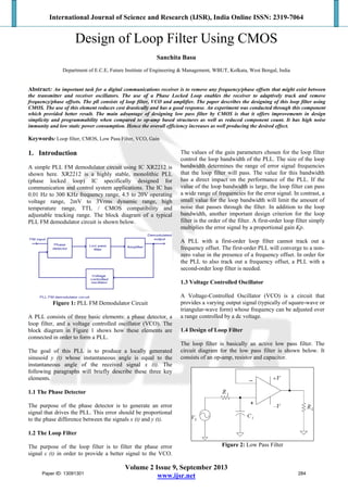
  • 1. International Journal of Science and Research (IJSR), India Online ISSN: 2319-7064 Volume 2 Issue 9, September 2013 www.ijsr.net Design of Loop Filter Using CMOS Sanchita Basu Department of E.C.E, Future Institute of Engineering & Management, WBUT, Kolkata, West Bengal, India Abstract: An important task for a digital communications receiver is to remove any frequency/phase offsets that might exist between the transmitter and receiver oscillators. The use of a Phase Locked Loop enables the receiver to adaptively track and remove frequency/phase offsets. The pll consists of loop filter, VCO and amplifier. The paper describes the designing of this loop filter using CMOS. The use of this element reduces cost drastically and has a good response. An experiment was conducted through this component which provided better result. The main advantage of designing low pass filter by CMOS is that it offers improvements in design simplicity and programmability when compared to op-amp based structures as well as reduced component count. It has high noise immunity and low static power consumption. Hence the overall efficiency increases as well producing the desired effect. Keywords: Loop filter, CMOS, Low Pass Filter, VCO, Gain 1. Introduction A simple PLL FM demodulator circuit using IC XR2212 is shown here. XR2212 is a highly stable, monolithic PLL (phase locked loop) IC specifically designed for communication and control system applications. The IC has 0.01 Hz to 300 KHz frequency range, 4.5 to 20V operating voltage range, 2mV to 3Vrms dynamic range, high temperature range, TTL / CMOS compatibility and adjustable tracking range. The block diagram of a typical PLL FM demodulator circuit is shown below. Figure 1: PLL FM Demodulator Circuit A PLL consists of three basic elements: a phase detector, a loop filter, and a voltage controlled oscillator (VCO). The block diagram in Figure 1 shows how these elements are connected in order to form a PLL. The goal of this PLL is to produce a locally generated sinusoid y (t) whose instantaneous angle is equal to the instantaneous angle of the received signal x (t). The following paragraphs will briefly describe these three key elements. 1.1 The Phase Detector The purpose of the phase detector is to generate an error signal that drives the PLL. This error should be proportional to the phase difference between the signals x (t) and y (t). 1.2 The Loop Filter The purpose of the loop filter is to filter the phase error signal ε (t) in order to provide a better signal to the VCO. The values of the gain parameters chosen for the loop filter control the loop bandwidth of the PLL. The size of the loop bandwidth determines the range of error signal frequencies that the loop filter will pass. The value for this bandwidth has a direct impact on the performance of the PLL. If the value of the loop bandwidth is large, the loop filter can pass a wide range of frequencies for the error signal. In contrast, a small value for the loop bandwidth will limit the amount of noise that passes through the filter. In addition to the loop bandwidth, another important design criterion for the loop filter is the order of the filter. A first-order loop filter simply multiplies the error signal by a proportional gain Kp. A PLL with a first-order loop filter cannot track out a frequency offset. The first-order PLL will converge to a non- zero value in the presence of a frequency offset. In order for the PLL to also track out a frequency offset, a PLL with a second-order loop filter is needed. 1.3 Voltage Controlled Oscillator A Voltage-Controlled Oscillator (VCO) is a circuit that provides a varying output signal (typically of square-wave or triangular-wave form) whose frequency can be adjusted over a range controlled by a dc voltage. 1.4 Design of Loop Filter The loop filter is basically an active low pass filter. The circuit diagram for the low pass filter is shown below. It consists of an op-amp, resistor and capacitor. Figure 2: Low Pass Filter Paper ID: 13091301 284
  • 2. International Journal of Science and Research (IJSR), India Online ISSN: 2319-7064 Volume 2 Issue 9, September 2013 www.ijsr.net A low-pass filter is a filter that passes low-frequency signals and attenuates (reduces the amplitude of) signals with frequencies higher than the cutoff frequency. The actual amount of attenuation for each frequency varies depending on specific filter design. The order of the filter determines the amount of additional attenuation for frequencies higher than the cut off frequency. The break frequency, also called the turnover frequency or cutoff frequency (in hertz), is determined by the time constant: fc=1/2πRC or equivalently (in radians per second): wc=1/RC 1.5 CMOS-Complementary Metal-Oxide-Semiconductor The term 'Complementary Metal-Oxide-Semiconductor', or simply 'CMOS', refers to the device technology for designing and fabricating integrated circuits that employ logic using both n- and p-channel MOSFET's. CMOS is the other major technology utilized in manufacturing digital IC's aside from TTL, and is now widely used in microprocessors, memories, and digital ASIC's. The input to a CMOS circuit is always to the gate of the input MOS transistor, which exhibits a very high resistance. This high gate resistance is due to the fact that the gate of a MOS transistor is isolated from its channel by an oxide layer, which is a dielectric. As such, the current flowing through a CMOS input is virtually zero, and the device is operated mainly by the voltage applied to the gate, which controls the conductivity of the device channel. Figure 3 2. Proposed Work The method proposed over here is the designing of low pass filter using CMOS. A first order low pass filter using CMOS is shown below- Figure 4: Magnitude plot for the 1st order filter Figure 5: Magnitude plot for the 1st order filter Figure 6: Second order low pass filter Figure 7: Magnitude plot for the 2nd order filter 3. Advantages of CMOS 1.The conventional operational amplifier (op-amp) is used as the active device in the vast majority of the active filter literature. A host of practical filter designs have evolved following this approach. It has also become apparent, however, that operational amplifier limitations preclude Paper ID: 13091301 285
  • 3. International Journal of Science and Research (IJSR), India Online ISSN: 2319-7064 Volume 2 Issue 9, September 2013 www.ijsr.net the use of these filters at high frequencies, attempts to integrate these filters have been unsuccessful (with the exception of a few no demanding applications), and convenient voltage or current control schemes for externally adjusting the filter characteristics do not exist. 2.These structures offer improvements in design simplicity and programmability when compared to op-amp based structures as well as reduced component count. 3.All transistors in the circuit are operated in the weak inversion region so that the low supply voltage and very low power consumption is also achieved. 4.Two important characteristics of CMOS devices are high noise immunity and low static power consumption. Since one transistor of the pair is always off, the series combination draws significant power only momentarily during switching between on and off states. 5.Consequently, CMOS devices do not produce as much waste heat as other forms of logic, for example transistor– transistor logic (TTL) or NMOS logic, which normally have some standing current even when not changing state. 4. Observations and Result Analysis 4.1 Gain Plot of 1st order Low Pass Filter Figure 8: Gain Plot of 1st order Low Pass Filter 4.2 Theoretical Result cut-off frequency fc=1/(2πR1C1). So, the theoretical value of cut-off frequency of 1st order low pass filter is fc=1/ (2π*10K*0.01uF) fc=1.59Khz 4.3 Gain Plot of 2nd Order LPF Figure 9: Gain Plot of 2nd Order LPF 4.3 Theoretical Result Cut-off frequency fc=1/2π R1R2C1C2). So, from the practical circuit diagram the cut-off frequency of 2nd order low pass filter is fc=1/2π =1.59Khz. 5. Conclusion The MOS transistors in the designed Operational Trans- conductance Amplifier (OTA) operate in sub-threshold or weak inversion region, such that their drain currents are exponentially related to gate-to-source voltages, in the nA and even pA level. Sub-threshold CMOS circuit design is very difficult, since the governing equations that model the behavior of the MOS transistor in weak inversion are so complicated. The most advantageous aspect of sub-threshold design is that the supply voltage can be decreased below 1 V. Using minimum number of transistors and other active elements, the sub-threshold design leads to very low-power operation of the devices. These structures offer improvements in design simplicity and programmability when compared to op-amp based structures as well as reduced component count. 6. Future Work Due to the nature of wide screen topic, there are still several areas of Improvement for future work on this op-amp. One of the applications is described below: 6.1 CMOS as voltage controlled oscillator If you have a resistor that is referenced to the virtual ground of an operational amplifier, then it is easy to use a CMOS to make that resistance voltage controlled. The resistor is replaced by a voltage divider to the real ground so that the divider puts out about 5 mV, which gets connected to the positive input of the CMOS. The negative input is connected to ground as well, while the output of the CMOS goes into the virtual ground of the operational amplifier. The apparent resistance can then be controlled by adjusting I0 accordingly. Paper ID: 13091301 286
  • 4. International Journal of Science and Research (IJSR), India Online ISSN: 2319-7064 Volume 2 Issue 9, September 2013 www.ijsr.net Moreover it provides high noise immunity and low static power consumption. References [1] Solid State Devices by Neaman. [2] Operational Transconductance Amplifier by Archim Gratz. [3] A low frequency operational transconductance amplifier (OTA) design and band pass filter implementation using OTA-C filter topology by Aydin Ozyavas [4] CMOS transconductance amplifier, architectures and active filters: a tutorial by E.Sanchez- Sinencio and J.Silvia-Martinez [5] CMOS Analysis And Design by Sung-Mo Kang. [6] N. Bronstein and K. A. Semendjajew, Taschenbuch der Mathematik. BSB Teubner, [7] 24th ed., 1989. [8] D. Sauer, The LM13600 Story, May 2003. http://www.idea2ic.com. [9] H. Camenzind, Designing Analog Chips. Virtualbookworm.com Publishers, 2005. [10]http://www.designinganalogchips.com. [11]T. H. Wilmshurst, Analog Circuit Techniques with Digital Interfacing. Newnes, 2001. [12]Intersil Americas Inc., CA3080, CA3080A: 2MHz, Operational Transconductance Amplifier (OTA), Aug. 2004. FN475.6. Author Profile Sanchita Basu is currently pursuing B. Tech in Electronics & Communication Engineering at Future Institute of Engineering & Management under West Bengal University of Technology. Her research interest includes Control System and Radar Engineering. Paper ID: 13091301 287