1. 1
RF & Microwave Design and Measurement Laboratory
The University of Texas at Dallas
Ahnaf Hassan
Abstract: This lecture and lab course covered fundamentals of microwave design and measurements.
Various microwave components were designed and simulated with CAD tools (Microwave Office, AWR,
AXIEM) and then built and measured to compare performance with theory. The lab involved learning the
basics of accurate microwave measurements, including vector impedance (scattering parameters), scalar
measurements and spectrum analysis.
Keywords: Microwave Office, MWO, AWR, AXIEM, Vector Network Analyzer, VNA, S Parameters,
Resonators, Microstrip, EM Simulation, Power Divider, Coupler, Wilkinson, Filters, LNA, Amplifiers,
MMIC.
i. Introduction
RF components were designed according to given
goals, specified in terms of operating and cutoff
frequencies, gain, return and insertion losses etc.
Microwave Office was used to design and simulate
circuits and microwave implementations. The
components were then milled, and tested in the lab
using network analyzers, power meters etc.
Measured data was compared to simulated
(theoretical) data to test for accuracy and possible
design issues.
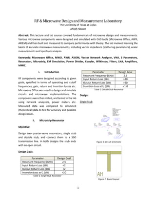
ii. Microstrip Resonator
Objective:
Design two quarter-wave resonators, single stub
and double stub, and connect them to a 50Ω
transmission line. In both designs the stub ends
with an open circuit.
Design Goal:
Parameter Design Goal
Resonant Frequency (GHz) 2.5
Input Return Loss (dB) <2
Output Return Loss (dB) <2
Insertion Loss at fo (dB) >20
Table 1: Single Stub Resonator
Parameter Design Goal
Resonant Frequency (GHz) 2.5
Input Return Loss (dB) >20
Output Return Loss (dB) >20
Insertion Loss at fo (dB) <1.0
Table 2: Double Stub Resonator
Design:
Single Stub
Figure 1: Circuit Schematic
Figure 2: Board Layout
MLEF
ID=TL4
W=2.96 mm
L=16.11 mm
MLIN
ID=TL1
W=2.96 mm
L=10 mm
MLIN
ID=TL3
W=2.96 mm
L=10 mm
MSUB
Er=4.45
H=1.57 mm
T=0.017 mm
Rho=0.705
Tand=0.02
ErNom=4.45
Name=SUB1
1 2
3
MTEE$
ID=TL2
MSUB=SUB1
STACKUP
Name=SUB2
EXTRACT
ID=EX1
EM_Doc="EM_Extract_Doc"
Name="EM_Extract"
Simulator=AXIEM
X_Cell_Size=1 mm
Y_Cell_Size=1 mm
STACKUP=""
Override_Options=Yes
Hierarchy=Off
SweepVar_Names=""
PORT
P=1
Z=50 Ohm
PORT
P=2
Z=50 Ohm
2. 2
Figure 3: Milled Design
Double Stub
Figure 4: Circuit Schematic
Figure 5: Board Layout
Figure 6: Milled Design
Performance:
Single Stub
Figure 7: Comparison of simulated and measured data
Double Stub
Figure 8: Comparison of insertion loss
1
2
3
4
MCROSS$
ID=TL2
MLEF
ID=TL4
W=2.96 mm
L=6.891 mm
MLEF
ID=TL5
W=2.96 mm
L=24.08 mm
MLIN
ID=TL1
W=2.96 mm
L=10 mm
MLIN
ID=TL3
W=2.96 mm
L=10 mm
MSUB
Er=4.45
H=1.57 mm
T=0.017 mm
Rho=0.705
Tand=0.02
ErNom=4.45
Name=SUB1
STACKUP
Name=SUB2
EXTRACT
ID=EX1
EM_Doc="EM_Extract_Doc"
Name="EM_Extract"
Simulator=AXIEM
X_Cell_Size=1 mm
Y_Cell_Size=1 mm
STACKUP=""
Override_Options=Yes
Hierarchy=Off
SweepVar_Names=""
PORT
P=1
Z=50 Ohm
PORT
P=2
Z=50 Ohm
1 2 3 4 5
Frequency (GHz)
Comparison between Measured and Simulated Data
-40
-30
-20
-10
0
2.5 GHz
-30.39 dB
2.5 GHz
-30.9 dB
2.5 GHz
-0.3817 dB
2.5 GHz
-0.4127 dB
DB(|S(1,1)|)
Single Stub Resonator AXIEM
DB(|S(2,2)|)
Single Stub Resonator AXIEM
DB(|S(2,1)|)
Single Stub Resonator AXIEM
DB(|S(1,1)|)
SS BETTER
DB(|S(2,2)|)
SS BETTER
DB(|S(2,1)|)
SS BETTER
3. 3
Figure 9: Comparison of return loss
iii. 3-dB Wilkinson Power Divider
Objective:
Design a microstrip 3-dB Wilkinson power
divider on 1.57mm thick FR-4 material and
compare and contrast simulated and
physical design.
Design Goal:
Parameter
Design
Goal
Center Frequency (GHz) 2.5
Power Split -3.0
Insertion Loss <1.0
Relative Phase 0
Input Return Loss >20
Output Return Loss >20
Isolation between Output Ports >20
Table 3: Design goals
Design:
Figure 10: Circuit design
Figure 11: Board layout
Figure 12: Milled design
Performance:
Figure 13: Comparison of input return loss
MCURVE$
ID=TL5
ANG=90 Deg
R=0.775 mm
MSUB=SUB1
MCURVE$
ID=TL7
ANG=90 Deg
R=0.775 mm
MSUB=SUB1
MCURVE$
ID=TL8
ANG=90 Deg
R=1.48 mm
MSUB=SUB1
MCURVE$
ID=TL9
ANG=90 Deg
R=0.775 mm
MSUB=SUB1
MCURVE$
ID=TL10
ANG=90 Deg
R=0.775 mm
MSUB=SUB1
MCURVE$
ID=TL19
ANG=90 Deg
R=1.48 mm
MSUB=SUB1
MLIN
ID=TL1
W=2.96 mm
L=10 mm
MLIN
ID=TL3
W=1.55 mm
L=L1 mm
MLIN
ID=TL6
W=1.55 mm
L=L2 mm
MLIN
ID=TL11
W=1.55 mm
L=L3 mm
MLIN
ID=TL13
W=1.55 mm
L=L1 mm
MLIN
ID=TL14
W=2.96 mm
L=0.762 mm
MLIN
ID=TL15
W=1.55 mm
L=L2 mm
MLIN
ID=TL16
W=2.96 mm
L=10 mm
MLIN
ID=TL17
W=1.55 mm
L=L3 mm
MLIN
ID=TL18
W=2.96 mm
L=0.762 mm
MLIN
ID=TL20
W=2.96 mm
L=10 mm
MSUB
Er=4.45
H=1.57 mm
T=0.017 mm
Rho=0.705
Tand=0.02
ErNom=4.45
Name=SUB1
1
2
3 MTEE$
ID=TL2
MSUB=SUB1
1
2
3
MTEE
ID=TL4
W1=1.55 mm
W2=1.55 mm
W3=2.96 mm
MSUB=SUB1
1
2
3
MTEE
ID=TL12
W1=1.55 mm
W2=1.55 mm
W3=2.96 mm
MSUB=SUB1
RES
ID=R1
R=100 Ohm
STACKUP
Name=SUB2
EXTRACT
ID=EX1
EM_Doc="EM_Extract_Doc"
Name="EM_Extract"
Simulator=AXIEM
X_Cell_Size=1 mm
Y_Cell_Size=1 mm
STACKUP=""
Override_Options=Yes
Hierarchy=Off
SweepVar_Names=""
PORT
P=1
Z=50 Ohm
PORT
P=2
Z=50 Ohm
PORT
P=3
Z=50 Ohm
L3=4.93
L2=5.8
L1=6.9
1 2 3 4 5
Frequency (GHz)
Comparison of Input Retun Loss
-50
-40
-30
-20
-10
0
2.5 GHz
-29.59 dB
2.53 GHz
-29.9 dB
2.5 GHz
-21.73 dB
2.763 GHz
-41.19 dB
DB(|S(1,1)|)
S1TO2 UNTUNED
DB(|S(1,1)|)
Winkinson Milled AXIEM
4. 4
Figure 14: Comparison of insertion loss
Figure 15: Comparison of phase difference
iv. Microwave Directional Coupler
Objective:
Design a 3-dB Quadrature Branch-Line Directional
Coupler (not milled) and a microstrip Edge-Coupled
Coupler (20-dB coupling).
Design Goal:
Branch-line Coupler:
Parameter Design Goal
Center Frequency (GHz) 2.5
Coupling (dB) 3.0
Relative Phase (deg) 90
Input Return Losses(dB) >20
Isolation @fo (dB) TBD
Table 4: Design objectives
Edge-Coupled Coupler:
Parameter Design Goal
Center Frequency (GHz) 2.5
Coupling (dB) 20.0
Relative Phase (deg) 90
Input Return Loss (dB) >20
Isolation @fo (dB) TBD
Table 5: Design objectives
Design:
Branch-line Coupler:
Figure 16: Circuit layout
Edge-Coupled Coupler:
Figure 17: Circuit layout
1 2 3 4 5
Frequency (GHz)
Comparison of Insertion Loss
-6
-5.5
-5
-4.5
-4
-3.5
-3
2.5 GHz
-3.25 dB
2.5 GHz
-3.196 dB 2.5 GHz
-3.273 dB
2.5 GHz
-3.269 dB
DB(|S(2,1)|)
Winkinson Milled AXIEM
DB(|S(3,1)|)
Winkinson Milled AXIEM
DB(|S(2,1)|)
S1TO2 UNTUNED
DB(|S(2,1)|)
S1TO3 UNTUNED
1 2 3 4 5
Frequency (GHz)
Comparion of Output Port Phase Difference
-1
0
1
2
3
2.5 GHz
-0.07258 Deg
2.5 GHz
0.8491 Deg
SDeltaP(Winkinson Milled AXIEM,2,1,3,1) (Deg)
Winkinson Milled AXIEM
SDeltaP(S1TO3 UNTUNED,2,1,2,1) (Deg)
S1TO2 UNTUNED
MLIN
ID=TL1
W=W_Zo mm
L=L_Zo mm
1 2
3
MTEE
ID=TL2
W1=W_Zo mm
W2=W_Zosrt2_trans mm
W3=W_Zo_trans mm
MLIN
ID=TL3
W=W_Zosrt2_trans mm
L=L_Zosrt2_trans mm
1 2
3
MTEE
ID=TL4
W1=W_Zosrt2_trans mm
W2=W_Zo mm
W3=W_Zo_trans mm
MLIN
ID=TL5
W=W_Zo mm
L=L_Zo mm
MLIN
ID=TL6
W=W_Zo mm
L=L_Zo mm
12
3
MTEE
ID=TL7
W1=W_Zosrt2_trans mm
W2=W_Zo mm
W3=W_Zo_trans mm
MLIN
ID=TL8
W=W_Zo_trans mm
L=L_Zo_trans mm
MLIN
ID=TL9
W=W_Zosrt2_trans mm
L=L_Zosrt2_trans mm
12
3
MTEE
ID=TL10
W1=W_Zo mm
W2=W_Zosrt2_trans mm
W3=W_Zo_trans mm
MLIN
ID=TL11
W=W_Zo_trans mm
L=L_Zo_trans mm
MLIN
ID=TL12
W=W_Zo mm
L=L_Zo mm
MSUB
Er=4.45
H=1.57 mm
T=0.017 mm
Rho=0.705
Tand=0.02
ErNom=4.45
Name=SUB1
STACKUP
Name=SUB2
EXTRACT
ID=EX1
EM_Doc="EM_Extract_Doc"
Name="EM_Extract"
Simulator=AXIEM
X_Cell_Size=1 mm
Y_Cell_Size=1 mm
STACKUP=""
Override_Options=Yes
Hierarchy=Off
SweepVar_Names=""
PORT
P=1
Z=50 Ohm
PORT
P=2
Z=50 Ohm
PORT
P=3
Z=50 Ohm
PORT
P=4
Z=50 Ohm
W_Zo = 2.95984
L_Zo = 10
W_Zo_trans = 2.95984
L_Zo_trans=15.1
W_Zosrt2_trans = 5.07209
L_Zosrt2_trans=13.55
W
W
1
2
3
4
MCLIN
ID=TL4
W=Wd mm
S=Sep mm
L=L mm
MCURVE
ID=TL3
W=Wd mm
ANG=90 Deg
R=Ra mm
MCURVE
ID=TL5
W=Wd mm
ANG=90 Deg
R=Ra mm
MCURVE
ID=TL6
W=Wd mm
ANG=90 Deg
R=Ra mm
MCURVE
ID=TL8
W=Wd mm
ANG=90 Deg
R=Ra mm
MLIN
ID=TL1
W=Wd mm
L=L_feed mm
MLIN
ID=TL2
W=Wd mm
L=L_feed mm
MLIN
ID=TL7
W=Wd mm
L=L_feed mm
MLIN
ID=TL9
W=Wd mm
L=L_feed mm
MSUB
Er=2.2
H=1.57 mm
T=0.008 mm
Rho=0.705
Tand=0.0009
ErNom=2.2
Name=SUB1
STACKUP
Name=SUB2
EXTRACT
ID=EX1
EM_Doc="EM_Extract_Doc"
Name="EM_Extract"
Simulator=AXIEM
X_Cell_Size=1 mm
Y_Cell_Size=1 mm
STACKUP=""
Override_Options=Yes
Hierarchy=Off
SweepVar_Names=""
PORT
P=1
Z=50 Ohm
PORT
P=2
Z=50 Ohm
PORT
P=3
Z=50 Ohm
PORT
P=4
Z=50 Ohm
L_feed = 12
Ra = Wd/2
Wd=4.624384765625
L=24.0056840820313
Sep=1.84562629699707
5. 5
Figure 18: Board layout
Figure 19: Milled design
Performance:
Branch-line Coupler:
Figure 20: Coupling, insertion and return losses
Figure 21: Phase measurement
Edge-Coupled Coupler:
Figure 22: Comparison of coupling
Figure 23: Comparison of input return loss
Figure 24: Comparison of phase difference
v. Microstrip Filters
Objective:
Design a Chebychev 0.5dB ripple low pass filter and
a Butterworth low pass filter using microstrip lines.
1 2 3 4 5
Frequency (GHz)
Measurements
-40
-30
-20
-10
0
DB(|S(1,1)|)
3 dB Quadrature Coupler
DB(|S(2,1)|)
3 dB Quadrature Coupler
DB(|S(3,1)|)
3 dB Quadrature Coupler
DB(|S(3,2)|)
3 dB Quadrature Coupler
DB(|S(2,3)|)
3 dB Quadrature Coupler
DB(|S(4,1)|)
3 dB Quadrature Coupler
DB(|S(2,2)|)
3 dB Quadrature Coupler
DB(|S(3,3)|)
3 dB Quadrature Coupler
1 2 3 4 5
Frequency (GHz)
Relative Phase
0
50
100
150
200
2.5 GHz
89.78 Deg
SDeltaP(3 dB Quadrature Coupler,2,1,3,1) (Deg)
3 dB Quadrature Coupler
1 2 3 4 5
Frequency (GHz)
Comparison Coupled Port
-40
-35
-30
-25
-20
-15
-10
2.369 GHz
-19.2 dB
3.02 GHz
-19.01 dB
2.369 GHz
-19.17 dB
1.84 GHz
-18.93 dB
2.5 GHz
-19.24 dB
2.5 GHz
-19.1 dB
DB(|S(3,1)|)
Edge Coupled AXIEM
DB(|S(2,1)|)
P1TOP3
1 2 3 4 5
Frequency (GHz)
Comparison Input Return Loss at Port 1
-80
-60
-40
-20
0
2.5 GHz
-41.8 dB
2.5 GHz
-22.42 dB
2.9 GHz
-36.07 dB
2.395 GHz
-44.48 dB
DB(|S(1,1)|)
P1TOP3
DB(|S(1,1)|)
Edge Coupled AXIEM
1 2 3 4 5
Frequency (GHz)
Comparison Phase Difference
-100
-50
0
50
100
2.369 GHz
-86.2 Deg
2.369 GHz
-84.65 Deg
2.5 GHz
-85.88 Deg
2.5 GHz
-84.8 Deg
SDeltaP(Edge Coupled AXIEM,2,1,3,1) (Deg)
Edge Coupled AXIEM
SDeltaP(P1TOP3,2,1,2,1) (Deg)
P1TOP2
6. 6
Design Goal:
Chebychev:
Parameter Design Goal
Center Frequency, fc (GHz) 2.5
Ripple (dB) 0.5
Insertion Loss at 5GHz (2fc) (dB) >40
Table 6: Design parameters
Butterworth:
Parameter Design Goal
Center Frequency, fc (GHz) 2.5
Insertion Loss at 5GHz (2fc) (dB) >40
Table 7: Design parameters
Design:
Chebychev:
Figure 25: Circuit layout
Figure 26: 2D mesh layout
Figure 27: Milled design
Butterworth:
Figure 28: Circuit layout
Figure 29: 2D mesh layout
Figure 30: Milled design
Performance:
Chebychev:
Figure 31: Comparison of return loss at port 1
Figure 32: Comparison of return loss at port 2
MLEF
ID=TL5
W=4.12123 mm
L=7.99355 mm
MLEF
ID=TL7
W=4.12123 mm
L=7.99355 mm
MLIN
ID=TL1
W=2.95984 mm
L=10 mm
MLIN
ID=TL3
W=0.370715 mm
L=6.87825 mm
MLIN
ID=TL6
W=0.370715 mm
L=9.03204 mm
MLIN
ID=TL9
W=0.370715 mm
L=6.87825 mm
MLIN
ID=TL11
W=2.95984 mm
L=10 mm
MSTEP$
ID=TL2
MSTEP$
ID=TL10
MSUB
Er=4.45
H=1.57 mm
T=0.017 mm
Rho=0.705
Tand=0.02
ErNom=4.45
Name=SUB1
1 2
3
MTEE$
ID=TL4
MSUB=SUB1
1 2
3
MTEE$
ID=TL8
MSUB=SUB1
STACKUP
Name=SUB2
EXTRACT
ID=EX1
EM_Doc="EM_Extract_Doc"
Name="EM_Extract"
Simulator=AXIEM
X_Cell_Size=1 mm
Y_Cell_Size=1 mm
STACKUP=""
Override_Options=Yes
Hierarchy=Off
SweepVar_Names=""PORT
P=1
Z=50 Ohm
PORT
P=2
Z=50 Ohm
21
MLIN
ID=TL6
W=Wzh mm
L=L_2 mm
MSUB=SUB1
MLIN
ID=TL7
W=Wzl mm
L=C_1 mm
MSUB=SUB1
MLIN
ID=TL4
W=Wzh mm
L=L_4 mm
MSUB=SUB1
MLIN
ID=TL3
W=Wzl mm
L=C_3 mm
MSUB=SUB1
MLIN
ID=TL5
W=Wzl mm
L=C_3 mm
MSUB=SUB1
MSUB
Er=2.2
H=1.57 mm
T=0.008 mm
Rho=0.689
Tand=0.0009
ErNom=2.2
Name=SUB1
MLIN
ID=TL1
W=Wzl mm
L=C_1 mm
MSUB=SUB1
MLIN
ID=TL2
W=Wzh mm
L=L_2 mm
MSUB=SUB1
PORT
P=1
Z=50 Ohm
PORT
P=2
Z=50 Ohm
Zh = 80
Zl = 20
Wzl = 16.1814
C_1 = 2.37832
L_2 = 11.0609
C_3 = 10.2292
L_4 = 17.8139
Wzh = 2.20076
2 1
0.1 2.1 4.1 6.1 8
Frequency (GHz)
Chebychev Filter Comparison
-60
-40
-20
0
20
DB(|S(1,1)|)
CP1TOP2
DB(|S(1,1)|)
AXIEM
0.1 2.1 4.1 6.1 8
Frequency (GHz)
Chebychev Filter Comparison
-60
-40
-20
0
20
DB(|S(2,2)|)
CP1TOP2
DB(|S(2,2)|)
AXIEM
7. 7
Figure 33: Comparison of insertion loss
Figure 34: Ripples in the passband
Butterworth:
Figure 35: Comparison of return loss at port 1
Figure 36: Comparison of return loss at port 2
Figure 37: Comparison of insertion loss
vi. Microwave Amplifier
Objective:
Design a microwave RF amplifier using NEC32584C
transistor. To satisfy design, microstrip input and
output matching networks and a quarter
wavelength transformer need to be designed as
well. A feedback loop is to be designed using a
series capacitor and resistor.
Design Goals:
Parameter Design Goal
Frequency Range (GHz) 0.7 – 1.0
Liner Gain (dB) >8
Gain Flatness across band (dB) <1.0
Input Return Loss (dB) >15
Output Return Loss (dB) >15
VD (volts) 2
IDS (mA) 10
k-Factor (over 0.5-3GHz) >1
Table 8: Design requirements
0.1 2.1 4.1 6.1 8
Frequency (GHz)
Chebychev Filter Comparison
-60
-50
-40
-30
-20
-10
0
2.361 GHz
-1.338 dB
2.569 GHz
-1.24 dB
5 GHz
-42.04 dB
5.138 GHz
-48.11 dB
5 GHz
-50 dB
4.722 GHz
-42.11 dB
DB(|S(2,1)|)
CP1TOP2
DB(|S(2,1)|)
AXIEM
0.1 2.1 4.1 6.1 8
Frequency (GHz)
Chebychev Filter Comparison
-2
-1.5
-1
-0.5
0
0.1 GHz
-0.07592 dB
2.19 GHz
-0.8422 dB
2.423 GHz
-0.738 dB
1.94 GHz
-1.043 dB
2.083 GHz
-0.9812 dB
1.27 GHz
-0.3516 dB
1.275 GHz
-0.2913 dB
0.7343 GHz
-0.5429 dB
0.73 GHz
-0.5782 dB
2.361 GHz
-1.338 dB
2.569 GHz
-1.24 dB
DB(|S(2,1)|)
CP1TOP2
DB(|S(2,1)|)
AXIEM
0.1 2.1 4.1 6.1 8
Frequency (GHz)
Butterworth Filter Comparison
-60
-50
-40
-30
-20
-10
0
DB(|S(1,1)|)
BP1TOP2
DB(|S(1,1)|)
AXIEM
0.1 2.1 4.1 6.1 8
Frequency (GHz)
Butterworth Filter Comparison
-60
-50
-40
-30
-20
-10
0
DB(|S(2,2)|)
BP1TOP2
DB(|S(2,2)|)
AXIEM
0.1 2.1 4.1 6.1 8
Frequency (GHz)
Butterworth Filter Comparison
-40
-30
-20
-10
0
5 GHz
-25.21 dB
4.384 GHz
-28.15 dB
2.192 GHz
-3.104 dB
5 GHz
-19.64 dB
2.051 GHz
-3.039 dB
4.102 GHz
-26.25 dB
DB(|S(2,1)|)
BP1TOP2
DB(|S(2,1)|)
AXIEM
8. 8
Design:
Figure 38:Circuit layout
Figure 39: Board layout
Figure 40: Milled design
Performance:
Figure 41: Comparison of achievable gain
Figure 42: Comparison of input return loss
Figure 43: Comparison of output return loss
Figure 44: Comparison of stability (K-Factor)
vii. MMIC Filters on GaAs Substrate
Objective:
Design two MMIC Butterworth filters (low-pass and
high-pass) on GaAs substrate with a center
frequency of 5GHz while achieving maximum figure
CAP
ID=C1
C=4.7e-5 uF
MBENDA
ID=TL10
W=1.09176 mm
ANG=90 Deg
MSUB=SUB1
MBENDA
ID=TL12
W=1.09176 mm
ANG=90 Deg
MSUB=SUB1
MBENDA
ID=TL14
W=1.09176 mm
ANG=90 Deg
MSUB=SUB1
MBENDA
ID=TL16
W=1.09176 mm
ANG=90 Deg
MSUB=SUB1
MLIN
ID=TL2
W=2.95758 mm
L=10 mm
MSUB=SUB1
MLIN
ID=TL4
W=2.95758 mm
L=15 mm
MSUB=SUB1
MLIN
ID=TL7
W=1.09176 mm
L=10 mm
MSUB=SUB1
MLIN
ID=TL11
W=1.09176 mm
L=len mm
MSUB=SUB1
MLIN
ID=TL13
W=1.09176 mm
L=10 mm
MSUB=SUB1
MLIN
ID=TL15
W=1.09176 mm
L=len mm
MSUB=SUB1
MLIN
ID=TL17
W=1.09176 mm
L=5 mm
MSUB=SUB1
MSTEP
ID=TL3
W1=1.09176 mm
W2=2.95758 mm
MSUB=SUB1
MSUB
Er=4.45
H=1.57 mm
T=0.017 mm
Rho=0.705
Tand=0.02
ErNom=4.45
Name=SUB1
RES
ID=R1
R=250 Ohm
RES
ID=R2
R=250 Ohm
1 2
3
SUBCKT
ID=S1
NET="lab8v2"
PORT
P=1
Z=50 Ohm
PORT
P=2
Z=50 Ohm
len=6
100 3100 6100 8500
Frequency (MHz)
Gain Comparison
-20
-15
-10
-5
0
5
10
1000 MHz700 MHz
850 MHz
5.228 dB
850 MHz
9.51 dB
DB(|S(2,1)|)
Lab8
DB(|S(2,1)|)
AMPSS_PARAMETERS02
100 3100 6100 8500
Frequency (MHz)
Comparison of Input Return Loss
-50
-40
-30
-20
-10
0
1000 MHz700 MHz
1220 MHz
-5.996 dB
2168 MHz
-3.072 dB
DB(|S(1,1)|)
Lab8
DB(|S(1,1)|)
AMPSS_PARAMETERS02
100 3100 6100 8500
Frequency (MHz)
Comparison of Output Return Loss
-50
-40
-30
-20
-10
0
1000 MHz700 MHz
610 MHz
-11.6 dB
2890 MHz
-4.442 dB
DB(|S(2,2)|)
Lab8
DB(|S(2,2)|)
AMPSS_PARAMETERS02
100 3100 6100 8500
Frequency (MHz)
Comparison of Stability
-10
10
30
50
70
90
110
120
K()
Lab8
K()
AMPSS_PARAMETERS02
9. 9
of merit (small size and high rejection at 2fc) for
both designs.
Design Goals:
Parameter
Design
Goal
Cutoff Frequency (GHz) 5.0
Rejection at 2fc for low pass (dB) >25
Rejection at 0.5fc for high pass (dB) >25
Size Minimum
Cost Minimum
Figure of Merit, M Maximum
Table 9: Design goals for both filters
Design:
Low-pass Filter:
Figure 45: Circuit layout
Figure 46: Board layout
High-pass Filter:
Figure 47: Circuit layout
Figure 48: Board layout
Performance:
Low-pass Filter:
Figure 49: Insertion and return losses
High-pass Filter:
Figure 50: Insertion and return losses
- END -
MSUB
Er=12.9
H=150 um
T=2 um
Rho=1
Tand=0.0005
ErNom=12.9
Name=SUB1
TFC2
ID=TFC1
W=width um
L=len um
T=0.2 um
ER=6.8
RHO=1
TAND=0
MSUB=SUB1
TFC2
ID=TFC2
W=width um
L=len um
T=0.2 um
ER=6.8
RHO=1
TAND=0
MSUB=SUB1
12
3
MTEE$
ID=TL1
MSUB=SUB1
MVIA1P
ID=V1
D=60 um
H=150 um
T=2 um
W=100 um
RHO=1
MSUB=SUB1
12
3
MTEE$
ID=TL2
MSUB=SUB1
MVIA1P
ID=V2
D=60 um
H=150 um
T=2 um
W=100 um
RHO=1
MSUB=SUB1
MLIN
ID=TL3
W=12.5 um
L=100 um
MSUB=SUB1
MLIN
ID=TL4
W=width um
L=10 um
MSUB=SUB1
MLIN
ID=TL5
W=12.5 um
L=10 um
MSUB=SUB1
MLIN
ID=TL6
W=12.5 um
L=100 um
MSUB=SUB1
MLIN
ID=TL7
W=width um
L=10 um
MSUB=SUB1
MLIN
ID=TL8
W=12.5 um
L=100 um
MSUB=SUB1
MLIN
ID=TL9
W=100 um
L=100 um
MSUB=SUB1
MLIN
ID=TL10
W=100 um
L=100 um
MSUB=SUB1
MCINDS
ID=MSP1
NT=2.93
W=12.5 um
S=7.24 um
R=20.5 um
AB=0
WB=10 um
HB=2.06 um
LB=0 um
EPSB=1
TDB=0
TB=1.05 um
RhoB=1
MSUB=SUB1
MCINDS
ID=MSP3
NT=2.93
W=12.5 um
S=7.24 um
R=20.5 um
AB=0
WB=10 um
HB=2.06 um
LB=0 um
EPSB=1
TDB=0
TB=1.05 um
RhoB=1
MSUB=SUB1
MCINDS
ID=MSP2
NT=4.69
W=12.5 um
S=7.24 um
R=19.6 um
AB=0
WB=10 um
HB=1.97 um
LB=0 um
EPSB=1
TDB=0
TB=1.05 um
RhoB=1
MSUB=SUB1
MLIN
ID=TL12
W=12.5 um
L=10 um
MSUB=SUB1
MCURVE$
ID=TL11
ANG=90 Deg
R=10 um
MSUB=SUB1
MCURVE$
ID=TL13
ANG=-90 Deg
R=50 um
MSUB=SUB1
MSTEP$
ID=TL15
MSUB=SUB1
MLIN
ID=TL14
W=12.5 um
L=160 um
MSUB=SUB1
MLIN
ID=TL16
W=12.5 um
L=171 um
MSUB=SUB1
MSTEP$
ID=TL17
MSUB=SUB1
MCURVE$
ID=TL18
ANG=90 Deg
R=10 um
MSUB=SUB1
MLIN
ID=TL19
W=12.5 um
L=312 um
MSUB=SUB1
MVIA1P
ID=V4
D=60 um
H=150 um
T=2 um
W=100 um
RHO=1
MSUB=SUB1
MVIA1P
ID=V3
D=60 um
H=150 um
T=2 um
W=100 um
RHO=1
MSUB=SUB1
MCURVE$
ID=TL22
ANG=-90 Deg
R=10 um
MSUB=SUB1
MLIN
ID=TL23
W=12.5 um
L=230 um
MSUB=SUB1
MVIA1P
ID=V5
D=60 um
H=150 um
T=2 um
W=100 um
RHO=1
MSUB=SUB1
MVIA1P
ID=V6
D=60 um
H=150 um
T=2 um
W=100 um
RHO=1
MSUB=SUB1
PORT
P=1
Z=50 Ohm
PORT
P=2
Z=50 Ohm
len=59.79
width=54.99
MCINDS
ID=MSP1
NT=3.55
W=42.5 um
S=6.63 um
R=16.2 um
AB=0
WB=11.3 um
HB=2.18 um
LB=0 um
EPSB=1
TDB=0
TB=12.5 um
RhoB=1
MVIA1P
ID=V1
D=60 um
H=150 um
T=2 um
W=65 um
RHO=1
MSUB=SUB1
1 2
3
MTEE$
ID=TL1
TFC2
ID=TFC1
W=w um
L=l um
T=0.2 um
ER=6.8
RHO=1
TAND=0
MCINDS
ID=MSP2
NT=2.25
W=42.9 um
S=7.08 um
R=17.4 um
AB=0
WB=11.3 um
HB=2.21 um
LB=0 um
EPSB=1
TDB=0
TB=12.5 um
RhoB=1
MVIA1P
ID=V2
D=60 um
H=150 um
T=2 um
W=65 um
RHO=1
MSUB=SUB1
TFC2
ID=TFC2
W=w um
L=l um
T=0.2 um
ER=6.8
RHO=1
TAND=0
1 2
3
MTEE$
ID=TL2
1 2
3
MTEE$
ID=TL3
MCINDS
ID=MSP3
NT=3.55
W=42.5 um
S=6.63 um
R=16.2 um
AB=0
WB=11.3 um
HB=2.18 um
LB=0 um
EPSB=1
TDB=0
TB=12.5 um
RhoB=1MVIA1P
ID=V3
D=60 um
H=150 um
T=2 um
W=65 um
RHO=1
MSUB=SUB1
MLIN
ID=TL4
W=w um
L=10 um
MLIN
ID=TL5
W=w um
L=10 um
MSUB
Er=12.9
H=150 um
T=2 um
Rho=1
Tand=0.0005
ErNom=12.9
Name=SUB1
MLIN
ID=TL6
W=w um
L=200 um
MSUB=SUB1
MLIN
ID=TL7
W=w um
L=200 um
MSUB=SUB1
MLIN
ID=TL8
W=w um
L=200 um
MSUB=SUB1
MLIN
ID=TL9
W=w um
L=200 um
MSUB=SUB1
MLIN
ID=TL10
W=12.5 um
L=108.827 um
MSUB=SUB1
MLIN
ID=TL11
W=12.5 um
L=108.827 um
MSUB=SUB1
MLIN
ID=TL12
W=12.5 um
L=108.827 um
MSUB=SUB1
MCURVE$
ID=TL13
ANG=90 Deg
R=20 um
MSUB=SUB1
MLIN
ID=TL14
W=w um
L=100 um
MSUB=SUB1
MSTEP$
ID=TL15
MSUB=SUB1
MLIN
ID=TL16
W=100 um
L=100 um
MSUB=SUB1
MCURVE$
ID=TL17
ANG=90 Deg
R=20 um
MSUB=SUB1
MLIN
ID=TL18
W=w um
L=100 um
MSUB=SUB1
MLIN
ID=TL19
W=100 um
L=100 um
MSUB=SUB1
MSTEP$
ID=TL20
MSUB=SUB1
MVIA1P
ID=V4
D=60 um
H=150 um
T=2 um
W=wv um
RHO=1
MSUB=SUB1
MVIA1P
ID=V5
D=60 um
H=150 um
T=2 um
W=wv um
RHO=1
MSUB=SUB1
MVIA1P
ID=V6
D=60 um
H=150 um
T=2 um
W=wv um
RHO=1
MSUB=SUB1
MVIA1P
ID=V7
D=60 um
H=150 um
T=2 um
W=wv um
RHO=1
MSUB=SUB1
PORT
P=1
Z=50 Ohm
PORT
P=2
Z=50 Ohm
w=33.95
l=32.95
wv = 100
0.1 5.1 10.1 15
Frequency (GHz)
Low Pass Filter
-60
-50
-40
-30
-20
-10
0
0.1 GHz
-0.4531 dB
5 GHz
-3.641 dB
10 GHz
-33.98 dB
DB(|S(2,1)|)
LPF
DB(|S(1,1)|)
LPF
0.1 5.1 10.1 15
Frequency (GHz)
High Pass Filter
-200
-150
-100
-50
0
12.65 GHz
-0.2404 dB
2.5 GHz
-33.58 dB
5 GHz
-3.246 dB
DB(|S(2,1)|)
HPF
DB(|S(1,1)|)
HPF