2. MS-2374 Technical Article
Page 2 of 4
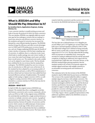
Figure 2. First Revision—JESD204A
Although both the original JESD204 standard and the
revised JESD204A standard were higher performance than
legacy interfaces, they were still lacking a key element. This
missing element was deterministic latency in the serialized
data on the link. When dealing with a converter, it is important
to know the timing relationship between the sampled signal
and its digital representation in order to properly recreate
the sampled signal in the analog domain once the signal has
been received (this situation is, of course, for an ADC, a
similar situation is true for a DAC). This timing relationship
is affected by the latency of the converter which is defined
for an ADC as the number of clock cycles between the instant
of the sampling edge of the input signal until the time that its
digital representation is present at the converter’s outputs.
Similarly, in a DAC, the latency is defined as the number of
clock cycles between the time the digital signal is clocked
into the DAC until the analog output begins changing. In the
JESD204 and JESD204A standards, there were no defined
capabilities that would deterministically set the latency of
the converter and its serialized digital inputs/outputs. In
addition, converters were continuing to increase in both
speed and resolution. These factors led to the introduction
of the second revision of the standard, JESD204B.
In July of 2011, the second and current revision of the standard,
JESD204B, was released. One of the key components of the
revised standard was the addition of provisions to achieve
deterministic latency. In addition, the data rates supported
were pushed up to 12.5 Gbps, broken down into different
speed grades of devices. This revision of the standard calls
for the transition from using the frame clock as the main
clock source to using the device clock as the main clock
source. Figure 3 gives a representation of the additional
capabilities added by the JESD204B revision.
Figure 3. Second (Current) Revision—JESD204B
In the previous two versions of the JESD204 standard, there
were no provisions defined to ensure deterministic latency
through the interface. The JESD204B revision remedies this
issue by providing a mechanism to ensure that, from power-
up cycle to power-up cycle and across link re-synchronization
events, the latency should be repeatable and deterministic.
One way this is accomplished is by initiating the initial lane
alignment sequence in the converter(s) simultaneously across
all lanes at a well-defined moment in time by using an input
signal called SYNC~. Another implementation is to use the
SYSREF signal which is a newly defined signal for JESD204B.
The SYSREF signal acts as the master timing reference and
aligns all the internal dividers from device clocks as well as
the local multiframe clocks in each transmitter and receiver.
This helps to ensure deterministic latency through the system.
The JESD204B specification calls out three device subclasses:
Subclass 0—no support for deterministic latency, Subclass 1—
deterministic latency using SYSREF, and Subclass 2—
deterministic latency using SYNC~. Subclass 0 can simply
be compared to a JESD204A link. Subclass 1 is primarily
intended for converters operating at or above 500 MSPS
while Subclass 2 is primarily for converters operating below
500 MSPS.
In addition to the deterministic latency, the JESD204B version
increases the supported lane data rates to 12.5 Gbps and
divides devices into three different speed grades. The source
and load impedance is the same for all three speed grades
being defined as 100 Ω ±20%. The first speed grade aligns
with the lane data rates from the JESD204 and JESD204A
versions of the standard and defines the electrical interface
for lane data rates up to 3.125 Gbps. The second speed grade
in JESD204B defines the electrical interface for lane data
rates up to 6.375 Gbps. This speed grade lowers the minimum
differential voltage level to 400 mV peak-to-peak, down from
500 mV peak-to-peak for the first speed grade. The third
speed grade in JESD204B defines the electrical interface for
lane data rates up to 12.5 Gbps. This speed grade lowers the
minimum differential voltage level required for the electrical
interface to 360 mV peak-to-peak. As the lane data rates
increase for the speed grades, the minimum required
3. Technical Article MS-2374
Page 3 of 4
differential voltage level is reduced to make physical
implementation easier by reducing required slew rates in
the drivers.
To allow for more flexibility, the JESD204B revision transitions
from the frame clock to the device clock. Previously, in the
JESD204 and JESD204A revisions, the frame clock was the
absolute timing reference in the JESD204 system. Typically,
the frame clock and the sampling clock of the converter(s)
were usually the same. This did not offer a lot of flexibility
and could cause undesired complexity in system design
when attempting to route this same signal to multiple
devices and account for any skew between the different
routing paths. In JESD204B, the device clock is the timing
reference for each element in the JESD204 system. Each
converter and receiver receives their respective device clock
from a clock generator circuit which is responsible for
generating all device clocks from a common source. This
allows for more flexibility in the system design but requires
that the relationship between the frame clock and device
clock be specified for a given device.
JESD204—WHY SHOULD WE PAY ATTENTION
TO IT?
In much the same way as LVDS began overtaking CMOS as
the technology of choice for the converter digital interface
several years ago, JESD204 is poised to tread a similar path
in the next few years. While CMOS technology is still hanging
around today, it has mostly been overtaken by LVDS. The
speed and resolution of converters as well as the desire for
lower power eventually renders CMOS and LVDS inadequate
for converters. As the data rate increases on the CMOS
outputs, the transient currents also increase and result in
higher power consumption. While the current, and thus,
power consumption, remains relatively flat for LVDS, the
interface has an upper speed bound that it can support.
This is due to the driver architecture, as well as the numerous
data lines that must all be synchronized to a data clock.
Figure 4 illustrates the different power consumption
requirements of CMOS, LVDS, and CML outputs for a dual
14-bit ADC.
Figure 4. CMOS, LVDS, and CML Driver Power Comparison
At approximately 150 MSPS to 200 MSPS and 14 bits of
resolution, CML output drivers start to become more
efficient in terms of power consumption. CML offers the
advantage of requiring less number of output pairs per a
given resolution than LVDS and CMOS drivers due to the
serialization of the data. The CML drivers specified for the
JESD204B interface have an additional advantage since the
specification calls for reduced peak-to-peak voltage levels as
the sample rate increases and pushes up the output line rate.
The number of pins required for the same give converter
resolution and sample rate is also considerably less. Table 1
gives an illustration of the pin counts for the three different
interfaces using a 200 MSPS converter with various channel
counts and bit resolutions. The data assumes a synchronization
clock for each channel’s data in the case of the CMOS and
LVDS outputs and a maximum data rate of 4.0 Gbps for
JESD204B data transfer using the CML outputs. The reasons
for the progression to JESD204B using CML drivers become
obvious when looking at this table and observing the dramatic
reduction in pin count that can be achieved.