[IJET-V2I3P17] Authors: R.C.Rohini, G.Srividhya

This project is proposed to integrate the Fuel cell emulator with a boost converter and load the DC motor and the performance analysis is done. Fuel cell as a renewable energy source is considered to be one of the most promising sources of electrical power. The characteristics of fuel cell is such that the DC power extracted from it is at low voltage level, this project proposes a prototype of a new power electronics based fuel cell emulator. After proposing a fuel cell emulator, it is integrated with a boost converter and DC motor is loaded. After the successful working of the boost converter, it can be directly connected with the actual Fuel Cell Systems (FCS) to satisfy the DC motor load which is integrated with fuel cell emulator and boost converter.

Recommandé
Recommandé
Contenu connexe
Tendances
Tendances (19)
En vedette
En vedette (16)
Similaire à [IJET-V2I3P17] Authors: R.C.Rohini, G.Srividhya
Similaire à [IJET-V2I3P17] Authors: R.C.Rohini, G.Srividhya (20)
Plus de IJET - International Journal of Engineering and Techniques
Plus de IJET - International Journal of Engineering and Techniques (20)
Dernier
Dernier (20)
[IJET-V2I3P17] Authors: R.C.Rohini, G.Srividhya
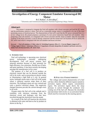
- 1. International Journal of Engineering and Techniques - Volume 2 Issue 3, May – June 2016 ISSN: 2395-1303 http://www.ijetjournal.org Page 102 Investigation of Energy Component Emulator Encouraged DC Motor R.C.Rohini1 , G.Srividhya2 , 1,2 (Electronics and Communication Department, Panimalar Engineering College, Chennai) I. INTRODUCTION Fuel cell technology is upcoming new electrical power technologies currently undergoing development. Fuel cell power systems have attracted attention because of their potential for high efficiency, low emissions, flexible use of fuels, and quiet operation. It has been recently developing amongst the manufactures in few years. The purpose of a fuel cell is to produce an electrical current that can be directed outside the cell to do work, such as powering an electric motor or illuminating a light bulb or a city. In general terms, hydrogen atoms enter a fuel cell at the anode where a chemical reaction strips them of their electrons. The hydrogen atoms are now ionized and carry a positive electrical charge. The negatively charged electrons provide the current through wires to do work. Oxygen enters the fuel cell at the cathode and it combines with electrons returning from the electrical circuit and hydrogen ions that have travelled through the electrolyte from the anode. As a result of the fuel cell reaction the electricity is obtained with water and heat as the by product as shown in the fig .1 Fig. 1 Working of fuel cell II. FUEL CELL CHARACTERISTICS The voltage and current characteristics of a fuel cell has a three distinctly different regions named as activation region, ohmic region, concentration region. The activation region shows the steep decrease in current through the conductor wire coming out of the fuel cell. Because the electrodes and electrolyte both involve in an activation barrier which must be overcome by the reacting species. RESEARCH ARTICLE OPEN ACCESS Abstract: This project is proposed to integrate the Fuel cell emulator with a boost converter and load the DC motor and the performance analysis is done. Fuel cell as a renewable energy source is considered to be one of the most promising sources of electrical power. The characteristics of fuel cell is such that the DC power extracted from it is at low voltage level, this project proposes a prototype of a new power electronics based fuel cell emulator. After proposing a fuel cell emulator, it is integrated with a boost converter and DC motor is loaded. After the successful working of the boost converter, it can be directly connected with the actual Fuel Cell Systems (FCS) to satisfy the DC motor load which is integrated with fuel cell emulator and boost converter. Keywords — Fuel cell emulator, δ= Duty ratio, fs= Switching frequency (Hz), ∆ = Current Ripple (Ampere),∆ = Voltage ripple (Volts),L= Inductance (Henry), C Capacitance (Farad), integration of emulator and boost converter, mimic Fuel cell characteristics, DC motor load.
- 2. International Journal of Engineering and Techniques - Volume 2 Issue 3, May – June 2016 ISSN: 2395-1303 http://www.ijetjournal.org Page 103 Fig. 2 VI characteristics of fuel cell Ohmic losses occur because of resistance to the flow of ions in the electrolyte and resistance to flow of electrons through the electrode materials. As a reactant is consumed at the electrode by electrochemical reaction, there is a loss of potential due to the inability of the surrounding material to maintain the initial concentration of the bulk fluid. That is, a concentration gradient is formed. Several processes may contribute to concentration region. The overall voltage developed from a fuel cell neglecting the losses is given by, V = E - Vact – Vohm – Vconcetration III. FUEL CELL EMULATOR Emulator is designed to mimic the characteristics of a fuel cell. We use a Buck converter to follow the linearly decreasing characteristics of fuel cell. With the help of potential divider to sense the load voltage (output voltage and current) and feed as input to the programmed PIC30F2020 chip. The resistance value measured in output is used to calculate duty cycle value. This duty cycle value controls the Buck converter switch and the corresponding V and I values similar to Fuel cell for the measured load is obtained. The DC-DC buck converter is operated at a constant frequency and a constant input DC voltage. The buck-converter is a circuit used to step-down a given value of dc voltage. When the transistor is in the "on" state, the diode is off and the current builds up through the inductor and the load. When the transistor is off, the current freewheels through the diode and decays. By properly choosing the on-off frequency and the inductor value, one achieves continuous current operation and the output voltage is then given by Vout = δVin Fig.3 Buck converter circuit A power MOSFET based DC-DC buck converter with switching frequency 50 kHz has been chosen. The design of the converter output filter has been carried out on the basis of the following assumptions: i. The components of the converter are ideal. ii. Operation of the converter is in continuous conduction mode. iii. No parasitic resistances. The above conditions lead to, = ∗ ∆ and = ∗ ∗ ∗∆ where, δ : Duty ratio fs: Switching frequency (Hz) ∆ : Current Ripple (Ampere) ∆ : Voltage ripple (Volts) L: Inductance (Henry) C: Capacitance (Farad) Since the emulator (buck converter) needs to mimic fuel cell, Buck converter duty cycle is not a constant as in regular buck operation. Duty cycle is governed by resistance measured from load side. Depending on the load requirement the pulse are generated and the buck converter produces the necessary dc level. We use the look-up table method to achieve the emulator characteristics: Lookup method: practical load values of fuel cell are taken and table is formed with resistance values and duty cycle (pdc) values. Program is written to produce pdc value corresponding to each resistance values. 15lpm fuel flow VI
- 3. International Journal of Engineering and Techniques - Volume 2 Issue 3, May – June 2016 ISSN: 2395-1303 http://www.ijetjournal.org Page 104 characteristics in steady state compared with the simulated and hardware results: For the 15lpm fuel flow the VI characteristics is plotted for the Hardware values and the simulated Buck converter model. The Hardware values and the simulated values are compared in the graph shown in fig .4 Fig.4 VI curve fitting characteristics for 15lpm plotted The below figure 5 shows the MATLAB model of the FCE as the Buck converter. Fig 5Matlab model of 1.2kW Buck converter The Buck converter model is designed in MATLAB which mimics the fuel cell characteristics in the closed loop system. The closed loop is made by the look-up table method and the results are achieved. The 1.2KW Buck converter model is designed with following the L&C values: L= 90uH C= 1880uF In the lookup table the output voltage and the current values are used as the inputs and they are converted as resistances. The lookup tables’ entries are the resistance values and the duty ratios of the Buck converter which are calculated. The output of the lookup table is given to the gate pulse of the MOSFET. By tuning the duty ratios we obtain the desired output values within the given range. Fig 6 lookup control for 1.2KW emulator The above fig 6 is the expansion of the sub- system which comprises of a function block to calculate the resistance and a lookup table block for generating the duty ratio corresponding to the resistance values. The duty ratio is compared with the repeating sequence of frequency 50 kHz. As a result we get a pulse of 50 kHz and desired duty ratio for the measured Buck output voltage and current. The simulated output of the fuel cell emulator as Buck converter is given in the fig 7. The voltage and current waveforms of the Buck converter is obtained. The closed loop control through the lookup table method achieves the fuel cell characteristics in the Buck converter. Fig 7 Fuel cell emulator output for variation in duty ratio The above fig 7 shows the output voltage and current level of a closed loop Buck converter simulated with a resistive load 2.85 ohms settling at 42.85V and 15.03A.
- 4. International Journal of Engineering and Techniques - Volume 2 Issue 3, May – June 2016 ISSN: 2395-1303 http://www.ijetjournal.org Page 105 A. Step change in load connected to emulator The simulation below is done to obtain the variation of the voltage level in the output of the emulator when a change in load in experienced with a change in the resistance. Fig 8 Step change in load of Fuel cell emulator block diagram Fig. 9 Output waveform showing change in load of Emulator for load current 3-5A and voltage of 51.5-50.5V The fuel cell characteristics show that it is a low voltage high current power source. Hence in order to supply high voltage applications such as the vehicular applications, a boost converter needs to be integrated with the fuel cell emulator, to test such applications. The boost circuit also consists of a control circuit in order to maintain the load voltage at a desired value, as may be required by the application. B. Boost converter The circuit diagram of boost converter is shown in Fig.9 A power MOSFET based DC-DC buck converter with switching frequency fs = 50 KHz has been chosen. Fig. 9 Boost converter L = ( VFCE * δ)/( fs *˄I) and C = (IFCE (1- δ) δ)/(fs *˄V) Where, L: Inductance (Henry) C: Capacitance (Farad) IFCE: Input current from FCE (Volts) VFCE: Input voltage from FCE (Volts) δ: Duty ratio fs: Switching frequency (Hz) ˄V : Voltage ripple (Volts) ˄I : Current Ripple (Ampere) The equivalent output resistance (Req) of the boost converter referred to the input side can be calculated as, Req = R(1- δ)2 The above equation is derived under ideal conditions. The value of Req corresponding to each of the operating points, can be used by the FCE, to fix upon an operating point using the change in duty ratio method. C. Simulation of boost converter open and closed loop controls The simulations of the boost converter in open and closed loop are given in the following fig 10 and 11. The open loop of the Boost converter is designed for the desired output voltage of 70V. The input voltage given to the Boost converter is within the range of 30-50V as it will be integrated with the fuel cell emulator in future chapters. Fig 10 Boost converter circuit in open loop
- 5. International Journal of Engineering and Techniques - Volume 2 Issue 3, May – June 2016 ISSN: 2395-1303 http://www.ijetjournal.org Page 106 The Boost inverter input voltage is in range if 30- 50 as mentioned above and it is designed to Boost the voltage up to 70V only. The inductor and capacitor is designed through the current ripple and voltage ripple methods. And the inductor and capacitor values are: L=63uH C=200uF Fig 11 Boost converter output voltage and current waveforms The boost converter is simulated in the closed loop as it has initial peak voltage and current values at the output side in open loop. In order to rectify the peak problem the closed loop control of Boost converter is done. The output voltage is taken as reference which is compared to the constant value and given to the PI input. The error signal from the PI controller is compared in the relational operator with the repeating sequence pulses. The output of the relational operator is given as the pulses for the MOSFET in the Boost converter. Fig 12 Boost closed loop control with PI controller Fig 13 Boost output voltage and current waveforms The above fig 13 shows the output voltage and current values of the Boost converter. Here the output voltage is maintained as desired for any resistive load given. D. Integrating a boost converter to the FCE The voltage level of Emulator is not sufficient to drive commercial loads. There comes the necessity of integration the FCE with a boost converter. The boost converter is also to be installed with a control circuit to maintain a constant voltage at its output terminals, irrespective of the current demand from the load. A feed forward technique of duty cycle control of the boost converter is used, to attain and sustain a constant voltage at the output terminals. Fig. 14Block diagram showing Boost converter integrated with Fuel cell Emulator We were able to simulate the integration FCE with boost converter of 50W configuration and now we have extended the simulation of 1.2kW configuration. In 1.2kW configuration we need to maintain the output voltage at 70 volts. The below output shows the regulated voltage as 70 volts.
- 6. International Journal of Engineering and Techniques ISSN: 2395-1303 Fig. 15 Simulation results showing the output voltage and output current of the Boost side of the integrated circuit of FCE with boost converter The integrated circuit with the Buck and the Boost converter is simulated and the results are obtained with the necessary voltage and current levels. The boost voltage is maintained to 72V. The integration of an emulator with a boost converter is simulated and the change in voltage levels for corresponding load change is obtained the figure.16. The hardware of the integration can be carried with the simulated component ratings. Fig.16 Block diagram of step change in load of integrated cir Fig 17. Output waveform at the Boost converter side for the step change in load (14.6-16.6ohms)(4.9-4.3A)(71V) International Journal of Engineering and Techniques - Volume 2 Issue 3, May – http://www.ijetjournal.org Fig. 15 Simulation results showing the output voltage and output current of the Boost side of the integrated circuit of FCE with boost converter The integrated circuit with the Buck and the e results are obtained with the necessary voltage and current levels. The boost voltage is maintained to 72V. The integration of an emulator with a boost converter is simulated and the change in voltage levels for corresponding load change is obtained in . The hardware of the integration can be carried with the simulated component ratings. change in load of integrated circuit Output waveform at the Boost converter side for the step change in The step change at the load side of the integrated circuit is done for different resistances 14.6 16.6ohms where the current reduces from 4.9 The voltage at the Boost side does not change since the Boost side is with voltage controller loop. Hence it maintains with a voltage of 71V in both the cases. E. Integrating circuit with DC motor load The integrated circuit is loaded with the DC motor as load which is the analysis that has to be done in this paper. The voltage and current values of the Buck and the Boost side varies when we put a DC motor load from resistive load. The difference is due to the RLE present in the DC motor motor ratings used here is: Power- 5HP Armature voltage- 240V Speed- 1740rpm Field- 150V The below block diagram [fig.18] represents the integrated circuit with the DC motor load. Fig.18 Block diagram representing the DC motor load with the integrated circuit The output waveform of the integrated circuit with the DC motor load is given below in the figure.19. It shows the voltage ripples that occur in the Buck and the Boost side with the DC motor load. – June 2016 Page 107 The step change at the load side of the integrated circuit is done for different resistances 14.6- 16.6ohms where the current reduces from 4.9-4.3A. voltage at the Boost side does not change since the Boost side is with voltage controller loop. Hence it maintains with a voltage of 71V in both motor load The integrated circuit is loaded with the DC which is the analysis that has to be done in this paper. The voltage and current values of the Buck and the Boost side varies when we put a DC motor load from resistive load. The difference the RLE present in the DC motor. The DC [fig.18] represents the integrated circuit with the DC motor load. Fig.18 Block diagram representing the DC motor load with the integrated output waveform of the integrated circuit with the DC motor load is given below in the figure.19. It shows the voltage ripples that occur in the Buck and the Boost side with the DC motor
- 7. International Journal of Engineering and Techniques ISSN: 2395-1303 Fig.19 Output waveform of the Buck side in the integrated ci motor load Fig.20 Output waveform of the Boost side in the integrated circuit with the DC motor load IV. CONCLUSIONS The further extension of this project can be done with any kind of machine to control the speed and current of the machine simultaneously by the loop processing. The closed loop control which is designed with the PI controller can be further designed with the same logic to control the system efficiently. The voltage ripple in the converter can be minimized using the effective filter technique. The hardware of the work can be implemented and the results can be verified with simulation results thus matching as the future work. ACKNOWLEDGMENT I extend my profound gratitude to tharamani for their support and guidance throughout the course of my work. I would also like to acknowledge the help I received from the technicians of Division of Power Electronics and Drives, DEEE. REFERENCES International Journal of Engineering and Techniques - Volume 2 Issue 3, May – http://www.ijetjournal.org Fig.19 Output waveform of the Buck side in the integrated circuit with DC Fig.20 Output waveform of the Boost side in the integrated circuit with the The further extension of this project can be done with any kind of machine to control the speed and ultaneously by the loop The closed loop control which is designed with the PI controller can be further designed with the same logic to control the system efficiently. The voltage ripple in the converter can be ilter technique. The hardware of the work can be implemented and the results can be verified with simulation results thus matching as the future work. I extend my profound gratitude to ACRI and guidance I would also like the help I received from the technicians of Division of Power Electronics and 1. VeeracharyMummadi,”Fuel cell effect for Non sources”, Third International Conference on Industrial and Information Systems 2008,IEEE 2. Yu-En Wu,Chih-Lung Shen,Chia-Yu Wu,” Research and Improvement of power enhancing for Photovoltaic Systems”,PEDS2009 3. Giuseppe Marsala et al, “Modelling and Implementation of an Emulator for Fuel Cell Systems Development of Control Strategies and Laws”, 2011 4. M.Rashid has discussed the design and analysis of a buck and a boost converter. 5. Sirisukprasert S., Seangsuwan T. (2010), “The Modelling and Control of Fuel Cell Emulator”, in Proc. ECTI 2010 6. T. Tafticht et al.,”An improved maximum power point tracking method for fuel cell systems”, Renewable Energy 33 (2008) 1508–1516. – June 2016 Page 108 VeeracharyMummadi,”Fuel cell effect for Non-linear DC onference on Industrial and Information Systems 2008,IEEE Yu Wu,” Research and Improvement of power enhancing for Photovoltaic Giuseppe Marsala et al, “Modelling and Implementation Cell Systems Development of Control Strategies and Laws”, 2011 M.Rashid has discussed the design and analysis of a buck Sirisukprasert S., Seangsuwan T. (2010), “The Modelling and Control of Fuel Cell Emulator”, in Proc. ECTI - CON, T. Tafticht et al.,”An improved maximum power point tracking method for fuel cell systems”, Renewable Energy