
Recommandé
Contenu connexe
Tendances
Tendances (20)
Similaire à Epitaxy
Similaire à Epitaxy (20)
Plus de ImranAhmad225
Dernier
Dernier (20)
Epitaxy
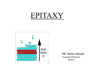
- 1. EPITAXY Mr. Imran ahmad Assistant Professor JETGI
- 2. 1) Epitaxy refers to the method of depositing a mono- crystalline film on a mono-crystalline substrate. The deposited film is denoted as epitaxial film or epitaxial layer. 2) The term epitaxy comes from the Greek roots, Epi means “above” and taxis means “deposition in ordered manner”. 3) Epitaxial films may be grown from gaseous or liquid precursors. 4) The substrate acts as a seed crystal, the deposited film takes on a lattice structure and orientation identical to those of the substrate.
- 3. Types of Epitaxial films Epitaxial films can be classified into two broad categories: (1)Homoepitaxy -The film and the substrate are the same material. -Epitaxially grown layers are purer than the substrate and can be doped independently of it. (2)Heteroepitaxy- Film and substrate are of different materials
- 4. • Atomic layer deposition (ALD) is a thin film deposition technique that is based on the sequential use of a gas phase chemical process. • ALD is considered a subclass of chemical vapour deposition. The majority of ALD reactions use two chemicals, typically called precursors. • These precursors react with the surface of a material one at a time in a sequential, self-limiting, manner. • Through the repeated exposure to separate precursors, a thin film is slowly deposited. VAPOR -PHASE EPITAXY
- 5. Advantages • VPE provides a very controlled method to produce a film to an atomically specified thickness. Also, the growth of different multilayer structures is straightforward. • Due to the sensitivity and precision of the equipment, it is very beneficial to those in the field of microelectronics and nanotechnology in producing small, but efficient semiconductors Disadvantages • High purity of the substrates is very important, and as such, high costs will ensue • Once the layer has been made and the process is complete, there may be a requirement of needing to remove excess precursors from the final product.
- 6. Molecular Beam Epitaxy • To make an interesting new crystal using MBE, you start off with a base material called a substrate, which could be a familiar semiconductor material such as silicon, germanium, or gallium arsenide • First, you heat the substrate, typically to some hundreds of degrees (for example, 500–600°C or about 900–1100°F in the case of gallium arsenide) • Then you fire relatively precise beams of atoms or molecules (heated up so they're in gas form) at the substrate from "guns" called effusion cells • The molecules land on the surface of the substrate, condense, and build up very slowly and systematically in ultra-thin layers, so the complex, single crystal you're after grows one atomic layer at a time • That's why MBE is an example of what's called thin-film deposition
- 7. Basic elements of MBE system: • Heated substrate • Effusion cells and shutter • Reflection High Energy Electron • Diffraction (RHEED system- RHEED gun & screen) • Ultra High Vacuum (UHV) • Liquid Nitrogen cryopanelling
- 8. • The solid source material sublimates • They provide angular distribution of atoms or molecules in beam • The substrate is heated to the necessary temperature • The gaseous elements then condense on the wafer where they may react with each other to form a layer • Atoms on clean surface are free to move until finding correct position in the crystal lattice to bond PROCESS
- 9. Advantages and Disadvantages of MBE Advantages: It's particularly good for making high-quality (low-defect, highly uniform) semiconductor crystals from compounds or from a number of different elements, instead of from a single element It also allows extremely thin films to be fabricated in a very precise, carefully controlled way Disadvantages: It's a slow and laborious method (crystal growth rate is typically a few microns per hour), which means it's more suited for scientific research laboratories than high-volume production, and the equipment involved is complex and very expensive (partly because of the difficulty of achieving such clean, high vacuum conditions)