
Recommandé
Contenu connexe
Similaire à PCB manufacture design rule
Similaire à PCB manufacture design rule (20)
Dernier
Dernier (20)
PCB manufacture design rule
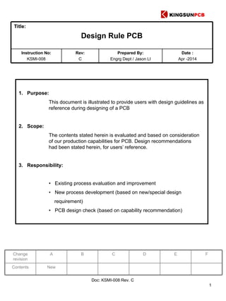
- 1. Title: Design Rule PCB Instruction No: KSMI-008 Rev: C Prepared By: Engrg Dept / Jason LI Date : Apr -2014 1. Purpose: This document is illustrated to provide users with design guidelines as reference during designing of a PCB 2. Scope: The contents stated herein is evaluated and based on consideration of our production capabilities for PCB. Design recommendations had been stated herein, for users’ reference. 3. Responsibility: • Existing process evaluation and improvement • New process development (based on new/special design requirement) • PCB design check (based on capability recommendation) Change revision A B C D E F Contents New Doc: KSMI-008 Rev. C 1
- 2. Title: Design Rule PCB Instruction No: KSMI-008 Rev: C Prepared By: Engrg Dept / Jason LI Date : Apr -2014 Contents No Description Pg 1. Laminate type 7 2. Laminate size 7 3. Board cut 8 4. Circuits 5. NC Drill b. Spacing between solder pads to land/ground 9 a. Minimum line width and spacing 9 c. Hole to track or land spacing 10 d. Outline to track location 10 e. V-cut Line to track and Land 11 f. Finished Track width tolerance 12 g. Finished track spacing tolerance 12 h. Annular ring 12 i. Dummy pattern 12 a. Drill stack 13 b. Drill direction 13 c. NC drill capability 13 Doc: KSMI-008 Rev. C 2
- 3. Title: Design Rule PCB Instruction No: KSMI-008 Rev: C Prepared By: Engrg Dept / Jason LI Date : Apr -2014 Contents No Description Pg 5. NC Drill (Cont’d) 6. Solder mask e. Hole to outline and tolerance 14 f. NC drill size 14 g. Hole edge to hole edge spacing 15 h. Hole to v-cut line spacing 15 i. Routing hole / slot 15 d. Hole position tolerance 13 a. Soldermask colour 16 b. Soldermask supplier 16 c. Soldermask thickness 16 d. Working panel size 17 e. Soldermask opening design 17 f. Soldermask opening 17 g. Soldermask mis-registration 18 h. Soldermask legends width, spacing and height 18 i. Soldermask bridge 19 j. LED soldermask opening and ground pad design 20 Doc: KSMI-008 Rev. C 3
- 4. Title: Design Rule PCB Instruction No: KSMI-008 Rev: C Prepared By: Engrg Dept / Jason LI Date : Apr -2014 Material Type Base Laminate Thickness (+/-) 1 0.2+/-0.038mm (Copper H/H,1/1oz) 2 0.25+/-0.038mm (Copper H/H,1/1oz) 3 0.36+/-0.05mm (Copper H/H,1/1oz) 4 0.41+/-0.05mm (Copper H/H,1/1oz) 5 0.51+/-0.064mm (Copper H/H,1/1oz) 6 0.61+/-0.064mm (Copper H/H,1/1oz) 7 0.71+/-0.064mm (Copper H/H,1/1oz) 8 0.8+/-0.1mm (Copper H/H,1/1oz) 9 0.9+/-0.1mm (Copper H/H,1/1oz) 10 1.0+/-0.1mm (Copper H/H,1/1oz) 11 1.2+/-0.13mm (Copper H/H,1/1oz) 12 1.5+/-0.13mm (Copper H/H,1/1oz) 1.0 Base Laminate Thickness Available Standard Size Maximum Size Recommended Size 480mm x 580mm (18.9” x 22.83”) 530mm x 630mm (20.87” x 24.8”) 480mm x 580mm (18.9” x 22.83”) 2.0 Laminate Size Remark: If these circuits are solder pads, please add a 0.5mm spacing, as the solderpaste may overflow to the board edge and cause short circuit. Doc: KSMI-008 Rev. C 4
- 5. Title: Design Rule PCB Instruction No: KSMI-008 Rev: C Prepared By: Engrg Dept / Jason LI Date : Apr -2014 3.0 FR4 property according to IPC-4101 Item IPC-4101B/21(Normal Tg)) IPC-4101B/24(Middle Tg) IPC-4101B/26(High Tg) Tg (DSC) >=1100C >=1500C >=1700C Dk (@/MHZ) <=5.4 <=5.4 <=5.4 Df(@/MHZ) <=0.035 <=0.035 <=0.035 Absorb water T>=0.5mm,<=0.8% T>=0.5mm,<=0.8% T>=0.5mm,<=0.8% Dielectric breakdown T>=0.5mm,40KV T>=0.5mm,40KV T>=0.5mm,40KV Td(TGA) 300-3100c 300-3100c 300-3100c Anti-CAF NO NO YES CTI 175-225V 175-225V 175-225V T2600c 10min 10min 5min T2880c 1min 1min 0min T3000c 0 0 0 Z-CTE(before Tg) 50-70ppm 50-70ppm 50-70ppm Z-CTE(After Tg) 250-350ppm 250-350ppm 250-350ppm Rohs compliance YES YES YES Halogen free No,Br 18-21% No,Br 18-21% No,Br 18-21% Doc: KSMI-008 Rev. C 5
- 6. Title: Design Rule PCB Instruction No: KSMI-008 Rev: C Prepared By: Engrg Dept / Jason LI Date : Apr -2014 Item Reinforcement Resin system UL/ANSI Tg requirement Flame retardant Mechanism 1 CELLULOSE PAPER Phenolic XPC (HB),XXXPC NA N/A 2 CELLULOSE PAPER Phenolic FR1(V1),FR2 (V1) NA Bromine/Chlorine 3 CELLULOSE PAPER Epoxy FR3(V1) NA Bromine/Chlorine /Antimony oxide 4 Woven E- glass,Surface Cellulose paper,core Epoxy/Phenolic CEM-1 1000C(min) Bromine/Antimon y oxide 5 Woven E- glass,Surface Nonwoven E-galss core Epoxy CEM-3 NA Bromine 6 Woven E-Glass Epoxy G10 NA NA 7 Woven E-glass Difunctional epoxy Multifunctional epoxy FR4/21(V1) 1100C-1500C Bromine 8 Woven E-glass Epoxy,Hot strength rentention FR5/23(V1) 1350C-1850C Bromine 9 Woven E-glass Epoxy,Multifuncti onal Epoxy FR4/25(V1) 1500C-2000C Bromine 10 Woven E-glass Epox y ,Multifunctional Epoxy FR4/26(V1) 1700C-2200C Bromine 11 Woven E-galss Bismaleimide/Tri azine(BT) GPY/30(HB) 1700C-2200C Bromine 12 Woven E-glass Polymide GPY/40(HB) 2500C(min) NA 13 Woven E-glass Polymide/Epoxy GPY/42(HB) 2000C-2500C NA 4.0 Material composition instruction (Refer to IPC-4101) Doc: KSMI-008 Rev. C 6
- 7. Title: Design Rule PCB Instruction No: KSMI-008 Rev: C Prepared By: Engrg Dept / Jason LI Date : Apr -2014 5.0 Board cut AB C D E G Item A Min (D/s) 0.38m m Max (D/s) 2.8mm Min (ML) 0.6mm Max (ML) 2.8mm ite m 0.8mm<=T<=2.4 mm 2L<=L<=6L 0.4mm<=T<0.8mm 6L<L<=12L FX G 290X330mm<=FX G<=508x610mm 290X330mm<=FXG <=406x508mm 5.1 A&D are for delivery panel size length and width 5.2 The Minimum thickness and the maximum thickness With finished board thickness (Double side) 5.3 Working panel size base on thickness and layer Doc: KSMI-008 Rev. C 7
- 8. Title: Design Rule PCB Instruction No: KSMI-008 Rev: C Prepared By: Engrg Dept / Jason LI Date : Apr -2014 6.0 Inner layer process capability (Unit: mm) Doc: KSMI-008 Rev. C 8
- 9. Title: Design Rule PCB Instruction No: KSMI-008 Rev: C Prepared By: Engrg Dept / Jason LI Date : Apr -2014 7.0 Inner Circuits Item HOZ ,1OZ COPPER 2OZ COPPER 3OZ COPPER 4OZ COPPER A 4mil 7mil 10mil 12mil B 4mil 6mil 8mil 10mil C 4mil 7mil 10mil 12mil D 4mil 7mil 10mil 12mil Item HOZ ,1OZ COPPER 2OZ COPPER 3OZ COPPER 4OZ COPPER E 8mil 8mil 8mil 10mil G 5mil 8mil 10mil 12mil F 6mil 8mil 10mil 10mil 7.1 Spacing design A B C D E F G 7.2 Thermal pad design Remark: Thermal Line must be keep 2 line minimum Doc: KSMI-008 Rev. C 9
- 10. Title: Design Rule PCB Instruction No: KSMI-008 Rev: C Prepared By: Engrg Dept / Jason LI Date : Apr -2014 7.3 Spacing between copper to outline and V-cut line Item A (Supplier) A 15mil(min) B 20mil(Normal) A B A: Spacing between copper and outline B. Spacing between copper and V-cut line B B formula: 300C V-cut: 0.27mm V-cut depth+10mil 450C V-cut :0.42mm V-cut depth+10mil If A area have gold finger, need to be keep 20mil spacing from upper limited dimension Layer HOZ ,1OZ COPPER 2OZ COPPER 3OZ COPPER 4OZ COPPER 4L 6mil 8mil 10mil 12mil 6L 8mil 10mil 12mil 14mil 8L 8mil 10mil 12mil 14mil 10L 10mil 10mil 12mil 14mil 7.4 Annular ring manufacture c c: Internal annual ring Doc: KSMI-008 Rev. C 10
- 11. Title: Design Rule PCB Instruction No: KSMI-008 Rev: C Prepared By: Engrg Dept / Jason LI Date : Apr -2014 Supplier/L ayer 4layer 6layer 8layer 10layer A 7mil 8mil 9mil 10mil 7.5 Clearance Hole copper a. Clearance copper Normal line Isolated line HOZ 0.8-1.0mil 1.5mil 1OZ 1.2-1.5mil 2.0mil 2OZ 2.4-2.8mil 3.5mil 3OZ 3.6-4.0mil 4.5mil 4OZ 5.2mil 6.0mil 7.6 Compensation Doc: KSMI-008 Rev. C 11
- 12. Title: Design Rule PCB Instruction No: KSMI-008 Rev: C Prepared By: Engrg Dept / Jason LI Date : Apr -2014 8.0 NC drill capability Doc: KSMI-008 Rev. C 12
- 13. Title: Design Rule PCB Instruction No: KSMI-008 Rev: C Prepared By: Engrg Dept / Jason LI Date : Apr -2014 9.0 Hole design 9.1 Blind hole capability V figure count-Sink T figure Count- Sink 9.2 Count-Sink hole Manual NC drill( After Routing process or punching process) NC drill Machine (Before Routing or Punching process) V-figure count sink hole: need to be provide Angle, depth, Count sink and hole diameter T count sink hole: need to be provide count -sink hole size and count sink hole depth Doc: KSMI-008 Rev. C 13
- 14. Title: Design Rule PCB Instruction No: KSMI-008 Rev: C Prepared By: Engrg Dept / Jason LI Date : Apr -2014 B A Item Dimension Tolerance A 0.5-6.5mm +/-0.15mm B 0.15mm-Finished thickness +/-0.25mm a 600c,900c,1200c +/-50c V-figure 9.2.1 Count-sink hole capability and tolerance A BB Item Dimension Tolerance A 0.5(min) +/-0.15mm B 0.15mm to finished thickness +/-0.25mm T-figure a Doc: KSMI-008 Rev. C 14
- 15. Title: Design Rule PCB Instruction No: KSMI-008 Rev: C Prepared By: Engrg Dept / Jason LI Date : Apr -2014 10.0 PTH+PANEL PLATING+ Pattern plating capability Doc: KSMI-008 Rev. C 15
- 16. Title: Design Rule PCB Instruction No: KSMI-008 Rev: C Prepared By: Engrg Dept / Jason LI Date : Apr -2014 11.0 Outer circuit Doc: KSMI-008 Rev. C 16
- 17. Title: Design Rule PCB Instruction No: KSMI-008 Rev: C Prepared By: Engrg Dept / Jason LI Date : Apr -2014 Item Copper 2OZ 3OZ 4OZ Line width 8mil 12mil 14mil Line spacing 7mil 8mil 10mil Spacing between line to pads 7mil 8mil 10mil Spacing between pads to pads 7mil 8mil 10mil 11.1 Width and spacing of thick copper 11.2 Testing hole requirement Doc: KSMI-008 Rev. C 17
- 18. Title: Design Rule PCB Instruction No: KSMI-008 Rev: C Prepared By: Engrg Dept / Jason LI Date : Apr -2014 11.3 Annual ring Remark: - Base copper: hole tolerance +/- 0.076 mm. - HAL finishing: a) PTH hole without annual ring, easy peel off after HAL process. Min. 4mil annual ring requirement. b) PTH slot hole also easy peel off, suggest change NPTH. 11.4 Gold plating capability Remark: - Gold plating board, suggest the base copper is Hoz and plate to 1oz, hole copper thickness to copper+ Nickel+ Gold=0.8mil(min). - Gold plating is after solder mask process, the plating locations must be have extension line to board edge. Doc: KSMI-008 Rev. C 18
- 19. Title: Design Rule PCB Instruction No: KSMI-008 Rev: C Prepared By: Engrg Dept / Jason LI Date : Apr -2014 11.5 Patter plating and Etching Doc: KSMI-008 Rev. C 19
- 20. Title: Design Rule PCB Instruction No: KSMI-008 Rev: C Prepared By: Engrg Dept / Jason LI Date : Apr -2014 11.6 E-test after etching 11.7 Impedance control a b c Testing pin instruction Parameter be affected Impedance value: a) Line width (Top and bottom, Under cut locations) b) Copper thickness c) Dielectric constant d) Solder mask thickness e) Line spacing (Differential impedance control) f) Using polar software to calculate the impedance value Doc: KSMI-008 Rev. C 20
- 21. Title: Design Rule PCB Instruction No: KSMI-008 Rev: C Prepared By: Engrg Dept / Jason LI Date : Apr -2014 12.0 Solder Mask Supplier Type Color Enernal 780 series,790 series Green/Blue/Red/Yellow/white/B lack/Matt Green/Matt black/Matt white Tamura DSR2200 series Green/Blue/White/Black/Matt Green/Matt Black Taiyo PSM-800 series Green Unires PSR-200 series Green EMP EMP-110 Green Coates XU501T-4MXLU Matt Green Tamura halogen free solder mask DSR2200TT19BLHF, DSR2200TT19GHF Blue Green 12.1 Type & Color Remark: For Immersion Tin recommendation DSR2200( print 2 times) or resistance gold ink or PSR4000 ink. Doc: KSMI-008 Rev. C 21
- 22. Title: Design Rule PCB Instruction No: KSMI-008 Rev: C Prepared By: Engrg Dept / Jason LI Date : Apr -2014 12.2 Maximum working panel size is 470mm x 610mm 12.3 Board thickness is 0.4mm ~ 2.8mm 12.4 Solder mask opening design require A>=0.076mm Solder pad Solder mask opening Circuits trace a a a>=0.127mm(5mil) 12.5 Solder mask opening to circuits trace or ground copper spacing 12.6 Solder mask mis-registration capability: +/- 50um Doc: KSMI-008 Rev. C 22
- 23. Title: Design Rule PCB Instruction No: KSMI-008 Rev: C Prepared By: Engrg Dept / Jason LI Date : Apr -2014 12.7 Solder mark marking print: Width, Spacing and Height L U M I L E D S LL56.0238 A Legends width>=0.2mm Legends spacing A>=0.15mm Legends Height B>=1.5mm B a a A>=0.127mm - If base copper is HOZ, A=0.1mm and Immersion tin finishing board solder mask bridge is 0.127mm Copper ground Solder mask opening At ground copper, solder mask bridge design A>=0.127mm, if for finishing is Immersion Tin, suggested the spacing is 0.25mm 12.8 Solder mask bridge Doc: KSMI-008 Rev. C 23
- 24. Title: Design Rule PCB Instruction No: KSMI-008 Rev: C Prepared By: Engrg Dept / Jason LI Date : Apr -2014 Solder mask CopperBase laminate A B C Location Thickness (min) A 0.4mil B 0.2mil C 0.4mil 12.9 Thickness i) Print one time a. Solder mask thickness on circuits knee:0.2mil(min) b. Solder mask on circuits surface:0.4mil(min) ii) Print two times a. Solder mask thickness on circuits knee:0.4mil(min) b. Solder mask thickness on circuits surface:0.6mil(min) Doc: KSMI-008 Rev. C 24
- 25. Title: Design Rule PCB Instruction No: KSMI-008 Rev: C Prepared By: Engrg Dept / Jason LI Date : Apr -2014 12.10 Solder mask plugging hole Doc: KSMI-008 Rev. C 25
- 26. Title: Design Rule PCB Instruction No: KSMI-008 Rev: C Prepared By: Engrg Dept / Jason LI Date : Apr -2014 12.11 Solder mask cover for not plugging hole Doc: KSMI-008 Rev. C 26
- 27. Title: Design Rule PCB Instruction No: KSMI-008 Rev: C Prepared By: Engrg Dept / Jason LI Date : Apr -2014 13.0 Peel mask 13.1 Spacing between solder pad = > 12 mils. 13.2 Thickness - Print 1 times = 3~8 mils - Print 2 times = 5~15 mils 13.3 Print cover hole capability - Nilon stencil = < 40 mils - Aluminum stencil = < 72 mils Remark: If hole size more than 72 mils, have to use tape to cover 13.4 Peel mask with relative surface treatment. Number Surface treatment Peel mask (Yes/No) Cause and replacement 1 HAL/HAL Lead free YES NA 2 OSP/Flux No Use higher temperature tape 3 Immersion Gold YES NA 4 Gold plating YES NA 5 Immersion Tin NO Replace to higher temperature tape 6 Immersion sliver NO Replace to higher temperature tape Doc: KSMI-008 Rev. C 27
- 28. Title: Design Rule PCB Instruction No: KSMI-008 Rev: C Prepared By: Engrg Dept / Jason LI Date : Apr -2014 14.0 Legend Print 14.1 Color = White, Black, Yellow and Red. 14.2 Printing mis-registration = +/- 0.15mm. 14.3 Maximum working panel size = 470mm x 610mm 14.4 Board thickness = 0.4mm ~ 3.2mm 14.5 Minimum width and spacing = 0.15mm 14.6 Marking print to solder mask opening. A B C D Solder mask opening Copper pads w W=0.15mm 14.7 Marking print to outline and v-cut A B C D V-CUT Line Outline with routing or punching a b a. Width 0.5mm(min) b. Width 0.25mm(min) for Routing profile c. Width 0.3mm(min)) for Punching profile Doc: KSMI-008 Rev. C 28
- 29. Title: Design Rule PCB Instruction No: KSMI-008 Rev: C Prepared By: Engrg Dept / Jason LI Date : Apr -2014 14.7 Marking print to hole A B C D Hole a a>=0.15mm A B C D 1.5mm 14.8 Marking height AB Copper Legends AB Dielectric Legends A B OK Dielectric Not recommendedOK Legends 14.9 Marking allocation print Doc: KSMI-008 Rev. C 29
- 30. Title: Design Rule PCB Instruction No: KSMI-008 Rev: C Prepared By: Engrg Dept / Jason LI Date : Apr -2014 15.0 Carbon print 15.1 Type Brend: Xiong Zhen PR-800 Carbon resistance: <15ohm/Sq. 15.2 Capability Board thickness: 0.4 ~ 3.2mm Minimum trace width: 0.25mm Maximum board size: 406mm x 406mm Mis-registration tolerance: +/-0.15mm 15.3 Carbon print pad design: 15.4 Carbon print pad spacing design: Circuits pads 0.15mm(min) Carbon pads design A A>=0.4mm Carbon print to carbon print Doc: KSMI-008 Rev. C 30
- 31. Title: Design Rule PCB Instruction No: KSMI-008 Rev: C Prepared By: Engrg Dept / Jason LI Date : Apr -2014 Carbon print to circuits pad Carbon A>=0.38mm 15.5 Carbon print pad with solder mask opening Solder mask opening Copper pad 0.1mm(min) (Recommendation : 0.2mm) 15.6 Carbon printing thickness 1 time: 0.5mil-1.5mil 2 times: 0.8mil-2.6mil Doc: KSMI-008 Rev. C 31
- 32. Title: Design Rule PCB Instruction No: KSMI-008 Rev: C Prepared By: Engrg Dept / Jason LI Date : Apr -2014 16.0 Board finishing 16.1 Available finishing - HAL leaded - HAL lead free - Immersion Gold - Gold Plating - Immersion silver - Immersion Tin - Entek = Cu-106A (OSP) - WPF-21 (OSP) - Shikoku F2 (OSP) 16.2 Capability HAL finishing Number Item capability 1 Maximum working panel size 470mmx620mm 2 Board thickness range 0.4-3.2mm 3 HAL thickness in hole 0.1mil-2mil 4 HAL thickness in surface 0.03mil-1.5mil 5 Minimum hole size with HAL/HAL LF 0.35mm(Below will be have solder ball) 6 HAL Composition Tin 63%,lead 37%,Melt temperature 1830C 7 HAL Lead free compositions Tin:98.8%,Nickel:0.1- 0.8%,Copper:0.5-1.1%,Melt temperature:2230C Doc: KSMI-008 Rev. C 32
- 33. Title: Design Rule PCB Instruction No: KSMI-008 Rev: C Prepared By: Engrg Dept / Jason LI Date : Apr -2014 Number Item Capability 1 Working panel size 80x80mm to 470mmx620mm 2 Board thickness range 0.4mm-3.2mm 3 OSP thickness 0.2um-0.6um 4 OSP+ Gold finger WPF-21+Gold finger (Workable) 5 OSP finishing Number item Capability 1 Maximum working panel size 470mmx620mm 2 Board thickness range 0.4mm-3.2mm 3 Gold thickness 1-3u’’ 4 Nickel thickness 120u’’(min) 5 Not Availiable laminate NC drill board with FR1,R2,CEM-1 laminate, if have it, after immersion gold process 6 Availiable solder mask Liquid photo imageable Immersion gold Doc: KSMI-008 Rev. C 33
- 34. Title: Design Rule PCB Instruction No: KSMI-008 Rev: C Prepared By: Engrg Dept / Jason LI Date : Apr -2014 Number Item Capability 1 Working panel maximum dimension 406x520mm(Dimension exceed, add cut line) 2 Board thickness range 0.4mm-3.2mm 3 Gold thickness 10u’’-40u’’ 4 Nickel thickness 120u’’(min) 5 Gold composition Hard Gold 6 Gold finger contact line (Removed) 2nd,Bellving ,Add it in inner) 7 HAL (Or HAL lead free)+ Gold finger Ok process 8 OSP+GOLD FINGER OK,CAN PROCESS, BUT should be WPF+Gold finger 9 Immersion Tin+Gold finger A Reject/B OK/C OK 10 Immersion sliver+Gold finger Ok, process 11 Gold plating+ Gold finger OK,process 12 Immersion Gold+ Gold finger A Reject/B OK/C OK Gold finger Doc: KSMI-008 Rev. C 34
- 35. Title: Design Rule PCB Instruction No: KSMI-008 Rev: C Prepared By: Engrg Dept / Jason LI Date : Apr -2014 Num ber Item Capability 1 Working panel size 76x127mm- 470x620mm 2 Board thickness range 0.4mm-3.2mm 3 Sliver thickness 6-15u’’ 4 Baking Before Immersion sliver Immersion silver Num ber Item Capability 1 Working panel size 150x100mm to 400x550mm 2 Board thickness range 0.4mm to 3.2mm 3 Tin thickness 30u’’-50u’’ 4 Print solder mask times 2times(DSR22 00)Immersion tin Doc: KSMI-008 Rev. C 35
- 36. Title: Design Rule PCB Instruction No: KSMI-008 Rev: C Prepared By: Engrg Dept / Jason LI Date : Apr -2014 17.0 V-cut 17.1 Layout V-cut Line 17.2 Remain thickness Laminate Board thickness Remain thickness FR4 Laminate 0.8mm+/-0.1mm 0.30mm 1.0mm+/-0.13mm 0.35mm 1.20mm+/-0.13mm 0.35mm 1.6mm+/-0.15mm 0.4mm 2.0mm+/-0.2mm 0.6mm 2.4mm+/-0.24mm 0.7mm Doc: KSMI-008 Rev. C 36
- 37. Title: Design Rule PCB Instruction No: KSMI-008 Rev: C Prepared By: Engrg Dept / Jason LI Date : Apr -2014 Flow direction of V-grooving machine. S1 S2Jump v-cut S1:>8mm(min) S2:>8mm(min) S1 and S2 depth are not achieve to normal remain thickness If customer do not accept the enough depth, we can add slot at this location (See below ) Unit 1 Unit 2 Unit 3 V-cut line Suggest to Unit 1 Unit 2 Unit 3 17.3 Jump v-cut design Doc: KSMI-008 Rev. C 37
- 38. Title: Design Rule PCB Instruction No: KSMI-008 Rev: C Prepared By: Engrg Dept / Jason LI Date : Apr -2014 17.4 Between board edge to v-cut line design S: >/= 1.0mm 17.5 Design for auto-cut 7mm (min) 2mm (min) V-cut guide hole size: Diameter 3.175mm (NPTH 3X) V-cut guide hole to v-cut line spacing: 4mm (min) Doc: KSMI-008 Rev. C 38
- 39. Title: Design Rule PCB Instruction No: KSMI-008 Rev: C Prepared By: Engrg Dept / Jason LI Date : Apr -2014 17.6 V-cut between punching line design V-cut Line Routing or punching slot Not acceptable, because at Red location will be cause Burrs Recommended to V-cut Line Routing or punching slot Minimum:0.5mm Doc: KSMI-008 Rev. C 39
- 40. Title: Design Rule PCB Instruction No: KSMI-008 Rev: C Prepared By: Engrg Dept / Jason LI Date : Apr -2014 17.6 V-cut capability basic information Number Item capability 1 Working panel dimension 80x80mm to 406mmx406mm 2 Board thickness range <=0.8mm to 3.2mm(V-cut on both side),0.5-0.8mm(Single side V-cut) 3 Mis-registration on Top and bottom +/-0.1mm 4 Minimum V-cut spacing 4mm(min) 5 V-cut Angle 30+/-50c, 45+/-50c, 60+/-50c Doc: KSMI-008 Rev. C 40
- 41. Title: Design Rule PCB Instruction No: KSMI-008 Rev: C Prepared By: Engrg Dept / Jason LI Date : Apr -2014 18.0 Profile 18.1 Routing Number Item Capability 1 Working panel size 457mmx610mm 2 Routing bit size 0.7mm to 3.0mm 3 Internal radius R0.4mm to R1.6mm, Standard R1.0mm 4 NC drill to edge +/-0.127mm 5 Edging to edging +/-0.127mm 6 Routing Guide hole Minimum 2holes(NPTH) in delivery panel 7 Routing hole tolerance +/-0.127mm 8 Routing slot tolerance +/-0.127mm 9 NC drill (Hole or slot) to routing edge spacing 15mil(min) Board thickness:0.8mm-3.2mm A: >4mm, b: <=12mm, C: >=26mm Depth tolerance: L </= 56 MIL : +/-5MIL L >56mil : +/-8mil Leveling angle: 20-600C +/-50C Doc: KSMI-008 Rev. C 41
- 42. Title: Design Rule PCB Instruction No: KSMI-008 Rev: C Prepared By: Engrg Dept / Jason LI Date : Apr -2014 18.2 Punching Number Item Capability 1 Board thickness range 0.4mm-3.2mm 2 Maximum punching size 406x510mm 3 Minimum punching slot size 0.7mmx1.2mm 4 Punching Edge to hole in unit 1.2mm(min) 5 Minimum spacing between punching slot to punching Edge One board thickness 6 Punching Edge to Gold finger 35mil(min) Punching outline tolerance 0 ~ 100mm: +/-0.1mm 101mm ~ 200mm: +/-0.2mm 200mm ~ 300mm: +/-0.25mm Above 300mm: +/-0.3mm Doc: KSMI-008 Rev. C 42
- 43. Title: Design Rule PCB Instruction No: KSMI-008 Rev: C Prepared By: Engrg Dept / Jason LI Date : Apr -2014 19.0 E-Test 19.1 Parameter - Test voltage: 10V ~ 300V - continuity test resistance: 5 ohm ~ 15K ohm - Isolation resistance: 1M ohm ~ 100M ohm - Maximum testing size: 457x 610mm - Maximum probe points: 10224 points - Minimum testing point size: 6 mils - Minimum testing point pitch: 15 mils Remark: E-test net list generate from customer Gerber file Doc: KSMI-008 Rev. C 43
- 44. Title: Design Rule PCB Instruction No: KSMI-008 Rev: C Prepared By: Engrg Dept / Jason LI Date : Apr -2014 Doc: KSMI-008 Rev. C 44
- 45. Title: Design Rule PCB Instruction No: KSMI-008 Rev: C Prepared By: Engrg Dept / Jason LI Date : Apr -2014 Doc: KSMI-008 Rev. C 45
- 46. Title: Design Rule PCB Instruction No: KSMI-008 Rev: C Prepared By: Engrg Dept / Jason LI Date : Apr -2014 Doc: KSMI-008 Rev. C 46
- 47. Title: Design Rule PCB Instruction No: KSMI-008 Rev: C Prepared By: Engrg Dept / Jason LI Date : Apr -2014 Doc: KSMI-008 Rev. C 47